PL IA NT
Features
■ Superior circuit protection ■ Overcurrent and overvoltage protection ■ Blocks surges up to rated limits
E2 007 550 2
Applications
■ Set top box LNB ports ■ Protection modules and dongles ■ Process control equipment ■ Test and measurement equipment ■ General electronics
*R oH S
CO M
■ High speed performance ■ Small SMT package ■ RoHS compliant* ■ Agency recognition:
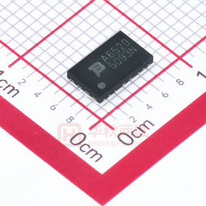
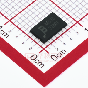
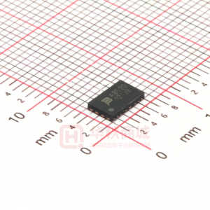
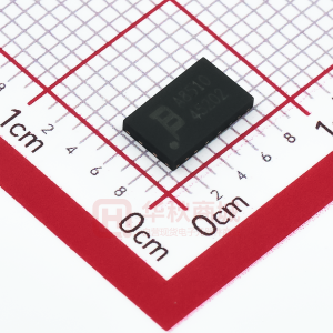
TBU-KE Series - TBU® High Speed Protectors
General Information The TBU-KE Series of Bourns® TBU® Line Side (Transient Blocking Unit) products are very low capacitance unidirectional high speed surge protection components designed to protect against faults caused by short circuits, AC power cross, induction and lightning surges.
1 2
Agency Approval
Load Side
Description UL File Number: E315805
TBU® Device
The TBU-KE is a unidirectional TBU® device: the TBU® protector will trip in less than 1 μs when the current reaches the maximum value in one direction only, that is when Pin 1 is positive in voltage with respect to Pin 2. No current limiting exists in the opposite polarity, and the TBU® protector appears as resistive in nature. The reverse current should not exceed the maximum trip current level of the TBU® device. An external diode may be used to prevent reverse current in DC biased applications. The TBU® protector blocks surges and provides an effective barrier behind which sensitive electronics will not be exposed to large voltages or currents during surge events. After the surge, the TBU® device resets when the voltage across the TBU® device falls to the Vreset level. The TBU® device will automatically reset on lines which have no DC bias or have DC bias below Vreset (such as unpowered signal lines). The TBU® device is provided in a surface mount DFN package and meets industry standard requirements such as RoHS and Pb Free solder reflow profiles.
Absolute Maximum Ratings (@ TA = 25 °C Unless Otherwise Noted)
Symbol Vimp Parameter Peak impulse voltage withstand with duration less than 10 ms Part Number TBU-KE025-xxx-WH TBU-KE040-xxx-WH TBU-KE050-xxx-WH TBU-KE025-xxx-WH TBU-KE040-xxx-WH TBU-KE050-xxx-WH Value 250 400 500 100 200 250 -40 to +85 -65 to +150 Unit V
Vrms Top Tstg
Continuous A.C. RMS voltage Operating temperature range Storage temperature range
V °C °C
Asia-Pacific: Tel: +886-2 2562-4117 • Fax: +886-2 2562-4116 Europe: Tel: +41-41 768 5555 • Fax: +41-41 768 5510 The Americas: Tel: +1-951 781-5500 • Fax: +1-951 781-5700 www.bourns.com
*RoHS Directive 2002/95/EC Jan 27, 2003 including Annex. Specifications are subject to change without notice. Customers should verify actual device performance in their specific applications.
�TBU-KE Series - TBU® High Speed Protectors
Electrical Characteristics (@ TA = 25 °C Unless Otherwise Noted)
Symbol Parameter Part Number TBU-KExxx-050-WH TBU-KExxx-100-WH TBU-KExxx-200-WH TBU-KExxx-300-WH TBU-KExxx-500-WH TBU-KE025-050-WH TBU-KE025-100-WH TBU-KE025-200-WH TBU-KE025-300-WH TBU-KE025-500-WH TBU-KE040-050-WH TBU-KE040-100-WH TBU-KE040-200-WH TBU-KE040-300-WH TBU-KE040-500-WH TBU-KE050-050-WH TBU-KE050-100-WH TBU-KE050-200-WH TBU-KE050-300-WH TBU-KE050-500-WH Min. 50 100 200 300 500 Typ. 75 150 300 450 750 12.5 6.3 3.4 2.4 1.8 13.0 6.8 3.9 3.0 2.3 13.7 7.5 4.6 3.6 3.0 Max. 100 200 400 600 1000 14.6 7.5 4.1 3.1 2.3 15.2 8.1 4.7 3.7 2.9 16.0 8.9 5.5 4.5 3.6 1 0.25 12 0.50 16 116 96 1.00 20 µs mA V °C/W °C/W Unit
Itrigger
Current required for the device to go from operating state to protected state
mA
Vimp = 250 V Vimp = 250 V Vimp = 250 V Vimp = 250 V Vimp = 250 V Vimp = 400 V Vimp = 400 V Vimp = 400 V Vimp = 400 V Vimp = 400 V Vimp = 500 V Vimp = 500 V Vimp = 500 V Vimp = 500 V Vimp = 500 V tblock IQ Vreset Rth(j-l) Rth(j-l)
Itrigger (min.) = Itrigger (min.) = Itrigger (min.) = Itrigger (min.) = Itrigger (min.) = Itrigger (min.) = Itrigger (min.) = Itrigger (min.) = Itrigger (min.) = Itrigger (min.) = Itrigger (min.) = Itrigger (min.) = Itrigger (min.) = Itrigger (min.) = Itrigger (min.) =
50 mA 100 mA 200 mA 300 mA 500 mA 50 mA 100 mA 200 mA 300 mA 500 mA 50 mA 100 mA 200 mA 300 mA 500 mA
Rdevice
Series resistance of the TBU® device
Ω
Time for the device to go from normal operating state to protected state Current through the triggered TBU® device with 50 Vdc circuit voltage Voltage below which the triggered TBU® device will transition to normal operating state Junction to package pads - FR4 using recommended pad layout Junction to package pads - FR4 using heat sink on board (6 cm2)
Specifications are subject to change without notice. Customers should verify actual device performance in their specific applications.
�TBU-KE Series - TBU® High Speed Protectors
Reference Application The TBU device can be used to protect against excessive voltage surges in DC biased equipment, as shown in the figure below. Diode D1 prevents reverse voltage surges from damaging the equipment, and the TBU® protector prevents any positive surges from causing damage. An overvoltage protection device, such as an MOV, may be used to provide additional overvoltage protection if the surge voltage is likely to be above the maximum rating of the TBU® device. D1 reverse voltage rating should be greater than that of the OVP device at the maximum surge current level. Typically, a 1N4007 is a suitable choice. D2 should be chosen to be above the normal working voltage of the protected device, but below its absolute maximum rating.
®
Basic TBU Operation The TBU® device is a silicon-based, solid-state, resettable device which is placed in series with a signal path. The TBU® device operates in approximately 1 µs - once line current exceeds the TBU® device’s trigger current Itrigger. When operated, the TBU® device restricts line current to less than 1 mA typically. When operated, the TBU® device will block all system voltages and any other voltages including the surge up to rated limits. After the surge, the TBU® device resets when the voltage across the TBU® device falls to the Vreset level. The TBU® device will automatically reset on lines which have no DC bias or have DC bias below Vreset (such as unpowered signal lines). If the line has a normal DC bias above Vreset, the voltage across the TBU® device may not fall below Vreset after the surge. In such cases, special care needs to be taken to ensure that the TBU® device will reset, otherwise an automatic or manual power down will be required. Bourns application engineers can provide further assistance.
D1
1
2
Line Side
OVP
D2
TBU® Device
Equip.
Performance Graphs V-I Characteristic - TBU-KE050-300-WH (Pin 2-1)
ITRIGGER
Typical Trigger Current vs. Temperature
1.8
Normalized Trip Current (A)
1.6 1.4 1.2 1.0 0.8 0.6 0.4 0.2 0.0 -75 -50 -25 0 25 50 75 100 125 150
CURRENT (100 mA/div.)
VRESET
VOLTAGE (5 v/div.)
Junction Temperature (°C)
Specifications are subject to change without notice. Customers should verify actual device performance in their specific applications.
�TBU-KE Series - TBU® High Speed Protectors
Performance Graphs (Continued) Power Derating Curve
3.0
Typical Resistance vs. Temperature
2.2
No additional PCB Cu 0.5 sq. in. additional PCB CU
2.5
Normalized Resistance (Ω)
140
2.0 1.8 1.6 1.4 1.2 1.0 0.8 0.6 0.4 0.2 0.0 -75 -50 -25
Total Max. Power (W)
2.0
1.5
1.0
0.5 0.0 20 40 60 80 100 120
0
25
50 75 100 125 150
Junction Temperature (°C)
Junction Temperature (°C)
Reflow Profile
Profile Feature Average Ramp-Up Rate (Tsmax to Tp) Preheat - Temperature Min. (Tsmin) - Temperature Max. (Tsmax) - Time (tsmin to tsmax) Time maintained above: - Temperature (TL) - Time (tL) Peak/Classification Temperature (Tp) Time within 5 °C of Actual Peak Temp. (tp) Ramp-Down Rate Time 25 °C to Peak Temperature Pb-Free Assembly 3 °C/sec. max. 150 °C 200 °C 60-180 sec. 217 °C 60-150 sec. 260 °C 20-40 sec. 6 °C/sec. max. 8 min. max.
Specifications are subject to change without notice. Customers should verify actual device performance in their specific applications.
�TBU-KE Series - TBU® High Speed Protectors
Product Dimensions
0.85 ± 0.05 (.033 ± .002) 5.00 ± 0.10 (.197 ± .004) 0.30 (.012) 0.60 (.024) 0.30 (.012) 0.75 (.030) 3.05 (.120)
2.50 ± 0.10 (.098 ± .004)
1.90 (.075)
PIN 1 & BACKSIDE CHAMFER
0.30 (.012)
C
0.25 PIN 1 (.010)
DIMENSIONS:
0.00 - 0.05 (.000 - .002)
MM (INCHES)
1.00 (.039)
Recommended Pad Layout TBU® protectors have matte-tin termination finish. The suggested layout should use Non-Solder Mask Define (NSMD). The recommended stencil thickness is 0.10-0.12 mm (.004.005 in.) with a stencil opening size 0.025 mm (.0010 in.) less than the device pad size. As when heat sinking any power device, it is recommended that wherever possible, extra PCB copper area is allowed. For minimum parasitic capacitance, do not allow any signal, ground or power signals beneath any of the pads of the device.
Thermal Resistance vs. Additional PCB Cu Area
100
Thermal Resistance to Ambient (°C/W)
90 80 70 60 50 40 30 20 10 0 0 0.2 0.4 0.6 0.8 1.0 1.2 1.4 1.6 1.8 2.0
Pad Designation Pad # 1
2 1
Pin Out Line Side Load Side
2
Added Cu Area (Sq. In.)
Dark grey areas show added PCB copper area for better thermal resistance.
Specifications are subject to change without notice. Customers should verify actual device performance in their specific applications.
�TBU-KE Series - TBU® High Speed Protectors
How to Order Typical Part Marking
TBU - KE 025 - 500 - WH
TBU Product Series KE = Uni-Series Impulse Voltage Rating 025 = 250 V 040 = 400 V 050 = 500 V Trigger Current 050 = 50 mA 100 = 100 mA 200 = 200 mA 300 = 300 mA 500 = 500 mA Hold to Trip Ratio Suffix W = Hold to Trip Ratio Package Suffix H = DFN Package
®
MANUFACTURER’S TRADEMARK
PRODUCT CODE - 1ST DIGIT INDICATES PRODUCT FAMILY: E = TBU-KE SERIES - 2ND & 3RD DIGITS INDICATE IMPULSE VOLTAGE: 25 = 250 V 40 = 400 V 50 = 500 V - 4TH & 5TH DIGITS INDICATE TRIGGER CURRENT: 05 = 50 mA 10 = 100 mA 20 = 200 mA 30 = 300 mA 50 = 500 mA
PIN 1 MANUFACTURING DATE CODE - 1ST DIGIT INDICATES THE YEAR’S 6-MONTH PERIOD. - 2ND DIGIT INDICATES THE WEEK NUMBER IN THE 6-MONTH PERIOD. - 3RD & 4TH DIGITS INDICATE SPECIFIC LOT FOR THE WEEK. 6-MONTH PERIOD CODES: A = JAN-JUN 2009 C = JAN-JUN 2010 B = JUL-DEC 2009 D = JUL-DEC 2010 E = JAN-JUN 2011 F = JUL-DEC 2011
Packaging Specifications
P0 E B t TOP COVER TAPE N D C F W D P2
A
B0 K0 A0 P G (MEASURED AT HUB) USER DIRECTION OF FEED CENTER LINES OF CAVITY D1 EMBOSSMENT
QUANTITY: 3000 PIECES PER REEL
A Min. 176 (6.929) A0 Min. 4.2 (.165) K0 Min. 1.1 (.043) Max. 1.3 (.051) Min. 7.9 (.311) Max. 4.4 (.173) Min. 6.65 (.262) P Max. 178 (7.008) Min. 1.5 (.059) B0
B Max. 2.5 (.098) D Max. 7.05 (.277) Max. 8.1 (.319) Min. 1.5 (.059) P0 Min. 3.9 (.159) Max. 4.1 (.161) Max. 1.6 (.063) Min. 12.8 (.504)
C Max. 13.5 (.531) D1 Min. 1.5 (.059) P2 Min. 1.9 (.075) Max. 2.1 (.083) Max. Min. 20.2 (.795)
D Max. E Min. 1.65 (.065) t Min. 0.25 (.010) Max. 0.35 (.014) Max. 1.85 (.073)
G Ref. 16.5 (.650) F Min. 7.4 (.291) W Min. 15.7 (.618)
DIMENSIONS:
N Ref. 102 (4.016)
max. 7.6 (.299) Max. 16.3 (.642)
MM (INCHES)
12/10
“TBU” is a registered trademark of Bourns, Inc. in the U.S., Taiwan and European Community. Specifications are subject to change without notice. Customers should verify actual device performance in their specific applications.
�
很抱歉,暂时无法提供与“TBU-KE040-050-WH”相匹配的价格&库存,您可以联系我们找货
免费人工找货- 国内价格
- 1+8.1536
- 10+6.8894
- 30+6.1936
- 国内价格
- 10+9.04
- 50+8.362
- 200+7.797
- 600+7.232
- 1500+6.78
- 3000+6.4975
- 国内价格
- 1+11.956
- 10+9.898
- 30+8.771
- 国内价格
- 1+9.9372
- 10+8.4966
- 30+7.7126
- 100+6.811