*R
oH
S
CO
M
PL
IA
NT
TISP4360H3BJ
BIDIRECTIONAL THYRISTOR OVERVOLTAGE PROTECTORS
TISP4360H3BJ Overvoltage Protector Series
Matched to FCC Part 68 POTS + ADSL Voltages
– Working Voltage, VDRM . . . . . . . . . . . . . . . . . . . . . 290 V
– Protection Voltage, V(BO) . . . . . . . . . . . . . . . . . . . . 360 V
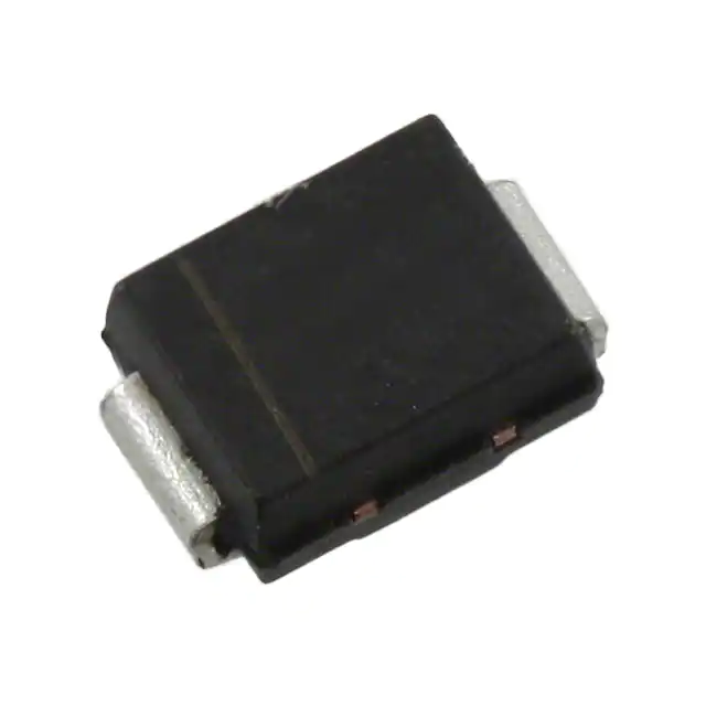
SMBJ Package (Top View)
High FCC, Bellcore & ITU-T Surge Ratings
Waveshape
Standard
2/10 µs
8/20 µs
10/160 µs
GR-1089-CORE
IEC 61000-4-5
FCC Part 68
ITU-T K.20/21
FCC Part 68
FCC Part 68
GR-1089-CORE
10/700 µs
10/560 µs
10/1000 µs
R(B) 1
2
T(A)
ITSP
A
500
300
250
MDXXBG
Device Symbol
200
T
160
100
High UL 1950, Bellcore & ITU-T AC Capability
Applied AC ‘4360 IT(OV)M Limit
A r.m.s.
s
40
0.04
UL 1950
7
4.2
(ANNEX NAC)
2.2
SURVIVES
0.015
60
0.08
30
GR-1089-CORE
0.48
15
SURVIVES
2.2
23
0.15
ITU-T K.20/21
1
SURVIVES
SD4XAA
Standard
R
Terminals T and R correspond to the
alternative line designators of A and B
Large creepage distance ............................... 2.54 mm (0.1 in.)
Low Capacitance ................................................... 24 pF @ 50 V
70 pF @ 0
.............................................. UL Recognized Component
Description
The TISP4360H3BJ is designed to limit overvoltages on equipment used for telephone lines carrying POTS (Plain Old Telephone System) and
ADSL (Asymmetrical Digital Subscriber Line) signals. TISP4360H3BJ a.c. overload limits are specified for designers to select the correct
overcurrent protectors to meet safety requirements, e.g. UL 1950.
The protector consists of a symmetrical voltage-triggered bidirectional thyristor. Overvoltages are initially clipped by breakdown clamping. If
sufficient current is available from the overvoltage, the breakdown voltage will rise to the breakover level, which causes the device to switch
into a low-voltage on-state condition. This switching action removes the high voltage stress from the following circuitry and causes the current
resulting from the overvoltage to be safely diverted through the protector. The high holding (switch off) current prevents d.c. latchup as the
diverted current subsides.
The TISP4360H3BJ is guaranteed to voltage limit and withstand the listed international lightning surges in both polarities. This high (H) current
protection device is in a plastic SMBJ package (JEDEC DO-214AA with J-bend leads) and supplied in embossed carrier reel pack. For
alternative voltage and holding current values, consult the factory.
How To Order
Device
Package
TISP4360H3BJ BJ (J-Bend DO-214AA/SMB)
Carrier
Embossed Tape Reeled
Order As
TISP4360H3BJR-S
*RoHS Directive 2002/95/EC Jan 27 2003 including Annex
JUNE 1999 - REVISED JANUARY 2007
Specifications are subject to change without notice.
Customers should verify actual device performance in their specific applications.
�TISP4360H3BJ Overvoltage Protector Series
Absolute Maximum Ratings, TA = 25 °C (Unless Otherwise Noted)
Rating
Repetitive peak off-state voltage, (see Note 1)
Non-repetitive peak on-state pulse current (see Notes 2, 3 and 4)
2/10 µs (GR-1089-CORE, 2/10 µs voltage wave shape)
8/20 µs (IEC 61000-4-5, 1.2/50 µs voltage, 8/20 current combination wave generator)
10/160 µs (FCC Part 68, 10/160 µs voltage wave shape)
5/200 µs (VDE 0433, 10/700 µs voltage wave shape)
0.2/310 µs (I3124, 0.5/700 µs voltage wave shape)
5/310 µs (ITU-T K.20/21, 10/700 µs voltage wave shape)
5/310 µs (FTZ R12, 10/700 µs voltage wave shape)
10/560 µs (FCC Part 68, 10/560 µs voltage wave shape)
10/1000 µs (GR-1089-CORE, 10/1000 µs voltage wave shape)
Non-repetitive peak on-state current (see Notes 2, 3 and 5)
20 ms (50 Hz) full sine wave
16.7 ms (60 Hz) full sine wave
1000 s 50 Hz/60 Hz a.c.
Maximum overload on-state current without open circuit, 50 Hz/60 Hz a.c.
0.015 s
0.04 s
0.08 s
0.15 s
0.48 s
4.2 s
Initial rate of rise of on-state current, Exponential current ramp, Maximum ramp value < 200 A
Junction temperature
Storage temperature range
NOTES: 1.
2.
3.
4.
5.
Symbol
Value
Unit
VDRM
±290
V
500
300
250
220
200
200
200
160
100
ITSP
A
55
60
2.2
ITSM
IT(OV)M
diT/dt
TJ
Tstg
A
60
40
30
23
15
7
400
-40 to +150
-65 to +150
A rms
A/µs
°C
°C
See Applications Information and Figure 9 for voltage values at lower temperatures.
Initially, theTISP4360H3BJ must be in thermal equilibrium with TJ = 25 °C.
The surge may be repeated after the TISP4360H3BJ returns to its initial conditions.
See Applications Information and Figure 10 for current ratings at other temperatures.
EIA/JESD51-2 environment and EIA/JESD51-3 PCB with standard footprint dimensions connected with 5 A rated printed wiring
track widths. See Figure 7 for the current ratings at other durations. Derate current values at -0.61 %/°C for ambient
temperatures above 25 °C.
Electrical Characteristics, T A = 25 °C (Unless Otherwise Noted)
V(BO)
Parameter
Repetitive peak offstate current
Breakover voltage
V(BO)
Impulse breakover
voltage
IDRM
I(BO)
VT
IH
dv/dt
ID
Breakover current
On-state voltage
Holding current
Critical rate of rise of
off-state voltage
Off-state current
Test Conditions
VD = VDRM
Min.
TA = 25 °C
TA = 85 °C
dv/dt = ±750 V/ms, RSOURCE = 300 Ω
dv/dt ≤ ±1000 V/µs, Linear voltage ramp,
Maximum ramp value = ±500 V
di/dt = ±20 A/µs, Linear current ramp,
Maximum ramp value = ±10 A
dv/dt = ±750 V/ms, RSOURCE = 300 Ω
IT = ±5 A, tW = 100 µs
IT = ±5 A, di/dt = -/+ 30 mA/ms
±0.15
±0.225
Linear voltage ramp, Maximum ramp value < 0.85VDRM
VD = ±50 V
JUNE 1999 - REVISED JANUARY 2007
Specifications are subject to change without notice.
Customers should verify actual device performance in their specific applications.
Typ.
Max.
±5
±10
±360
Unit
±372
V
±0.8
±3
±0.8
A
V
A
V
kV/µs
±5
TA = 85 °C
µA
±10
µA
�TISP4360H3BJ Overvoltage Protector Series
Electrical Characteristics, TA = 25 °C (Unless Otherwise Noted) (continued)
Parameter
Coff
Test Conditions
Off-state capacitance
f = 100 kHz,
f = 100 kHz,
f = 100 kHz,
f = 100 kHz,
f = 100 kHz,
Min.
Vd = 1 V rms, VD = 0,
Vd = 1 V rms, VD = -1 V
Vd = 1 V rms, VD = -2 V
Vd = 1 V rms, VD = -50 V
Vd = 1 V rms, VD = -100 V
Typ.
70
60
55
24
22
Max.
84
67
62
28
26
Unit
Typ.
Max.
Unit
pF
Thermal Characteristics
Parameter
RθJA
NOTE
Junction to free air thermal resistance
Test Conditions
Min.
EIA/JESD51-3 PCB, IT = ITSM(1000),
TA = 25 ° C, (see Note 6)
265 mm x 210 mm populated line card,
4-layer PCB, IT = ITSM(1000), TA = 25 °C
113
° C/W
50
6: EIA/JESD51-2 environment and PCB has standard footprint dimensions connected with 5 A rated printed wiring track widths.
JUNE 1999 - REVISED JANUARY 2007
Specifications are subject to change without notice.
Customers should verify actual device performance in their specific applications.
�TISP4360H3BJ Overvoltage Protector Series
Parameter Measurement Information
+i
Quadrant I
ITSP
Switching
Characteristic
ITSM
IT
V(BO)
VT
I(BO)
IH
VDRM
-v
IDRM
ID
VD
ID
IDRM
VD
VDRM
+v
IH
I(BO)
VT
V(BO)
IT
ITSM
Quadrant III
ITSP
Switching
Characteristic
-i
Figure 1. Voltage-current Characteristic for T and R Terminals
All Measurements are Referenced to the R Terminal
JUNE 1999 - REVISED JANUARY 2007
Specifications are subject to change without notice.
Customers should verify actual device performance in their specific applications.
PMXXAAB
�TISP4360H3BJ Overvoltage Protector Series
Typical Characteristics
OFF-STATE CURRENT
vs
JUNCTION TEMPERATURE
TCHAG
100
NORMALIZED BREAKOVER VOLTAGES
vs
JUNCTION TEMPERATURE
TC4HAF
1.10
VD = ±50 V
Normalized Breakover Voltage
|ID| - Off-State Current - µA
10
1
0·1
0·01
1.05
1.00
0.95
0·001
-25
0
25
50
75
100 125
TJ - Junction Temperature - °C
-25
150
Figure 2.
ON-STATE CURRENT
vs
ON-STATE VOLTAGE
200
150
TA = 25 °C
100
tW = 100 µs
NORMALIZED HOLDING CURRENT
vs
JUNCTION TEMPERATURE
TC4HACA
2.0
TC4HAK
1.5
Normalized Holding Current
IT - On-State Current - A
150
Figure 3.
70
50
40
30
20
15
10
7
5
4
3
1.0
0.9
0.8
0.7
0.6
0.5
2
1.5
1
0.7
0
25
50
75
100 125
TJ - Junction Temperature - °C
0.4
1
1.5
2
3
4 5
VT - On-State Voltage - V
Figure 4.
7
10
-25
0
25
50
75
100 125
TJ - Junction Temperature - °C
150
Figure 5.
JUNE 1999 - REVISED JANUARY 2007
Specifications are subject to change without notice.
Customers should verify actual device performance in their specific applications.
�TISP4360H3BJ Overvoltage Protector Series
Typical Characteristics
NORMALIZED CAPACITANCE
vs
OFF-STATE VOLTAGE
TC4HABA
1
0.9
TJ = 25 °C
Capacitance Normalized to VD = 0
0.8
Vd = 1 Vrms
0.7
0.6
0.5
0.4
0.3
0.2
0.5
1
2
3
5
10
20 30 50
VD - Off-state Voltage - V
Figure 6.
JUNE 1999 - REVISED JANUARY 2007
Specifications are subject to change without notice.
Customers should verify actual device performance in their specific applications.
100150
�TISP4360H3BJ Overvoltage Protector Series
30
NON-REPETITIVE PEAK ON-STATE CURRENT
vs
CURRENT DURATION
TI4HAC
70
60
50
40
VGEN = 600 Vrms, 50/60 Hz
RGEN = 1.4*VGEN/ITSM(t)
20
EIA/JESD51-2 ENVIRONMENT
EIA/JESD51-3 PCB
TA = 25 °C
15
I - RMS Current - A
ITSM(t) - Non-Repetitive Peak On-State Current - A
Rating and Thermal Information
10
9
8
7
6
5
4
3
1.5
0·1
10
100
EIA/JESD51-2 ENVIRONMENT
EIA/JESD51-3 PCB
TA = 25 °C
15
10
8
7
6
5
2
0·01
1000
RGEN = VGEN/IT(OV)M
20
3
2.5
1
VGEN = 600 Vrms, 50/60 Hz
30
25
4
2
MAXIMUM OVERLOAD ON-STATE CURRENT
vs
CURRENT DURATION
TI4HAJ
t - Current Duration - s
TISP4360H3BJ IT(OV)M
UL 1950 600 V rms
TESTS (1, 2 & 5)
0·1
1
10
t - Current Duration - s
Figure 7.
VDRM DERATING FACTOR
vs
MINIMUM AMBIENT TEMPERATURE
1.00
1000
Figure 8.
TI4HADA
700
600
0.99
IMPULSE RATING
vs
AMBIENT TEMPERATURE
TC4HAA
BELLCORE 2/10
500
400
Impulse Current - A
0.98
Derating Factor
100
0.97
0.96
0.95
IEC 1.2/50, 8/20
300
FCC 10/160
250
ITU-T 10/700
200
FCC 10/560
150
120
0.94
BELLCORE 10/1000
0.93
-40 -35 -30 -25 -20 -15 -10 -5 0 5 10 15 20 25
TAMIN - Minimum Ambient Temperature - °C
Figure 9.
100
90
-40 -30 -20 -10 0
10 20 30 40 50 60 70 80
TA - Ambient Temperature - °C
Figure 10.
JUNE 1999 - REVISED JANUARY 2007
Specifications are subject to change without notice.
Customers should verify actual device performance in their specific applications.
�TISP4360H3BJ Overvoltage Protector Series
APPLICATIONS INFORMATION
Deployment
These devices are two terminal overvoltage protectors. They may be used either singly to limit the voltage between two conductors (Figure 11)
or in multiples to limit the voltage at several points in a circuit (Figure 12).
Th3
Th1
Th1
Th2
Figure 11. Two Point Protection
Figure 12. Multi-point Protection
In Figure 11, protector Th1 limits the maximum voltage between the two conductors to ±V(BO). This configuration is normally used to protect
circuits without a ground reference, such as modems. In Figure 12, protectors Th2 and Th3 limit the maximum voltage between each conductor and ground to the ±V(BO) of the individual protector. Protector Th1 limits the maximum voltage between the two conductors to its ±V(BO)
value. If the equipment being protected has all its vulnerable components connected between the conductors and ground, then protector Th1
is not required.
Impulse Testing
To verify the withstand capability and safety of the equipment, standards require that the equipment is tested with various impulse wave forms.
The table below shows some common values.
Standard
Peak Voltage
Setting
V
Voltage
Waveform
µs
2/10
10/1000
10/160
10/560
9/720 †
9/720 †
0.5/700
Peak Current
Value
A
Current
Waveform
µs
TISP4360H3BJ
25 °C Rating
A
Series
Resistance
Ω
2500
500
2/10
500
0
1000
100
10/1000
100
1500
200
10/160
250
0
800
100
10/560
160
0
FCC Part 68
(March 1998)
1500
37.5
5/320 †
200
0
1000
25
5/320 †
200
0
I3124
1500
37.5
0.2/310
200
0
37.5
1500
5/310
200
0
ITU-T K.20/K. 21
10/700
100
4000
† FCC Part 68 terminology for the waveforms produced by the ITU-T recommendation K.21 10/700 impulse generator
GR-1089-CORE
Series resistance can be added to cover situations where either the TISP4360H3BJ current rating will be exceeded or excessive wiring
currents result or both.
When a primary protector is used, the TISP4360H3BJ may operate before the primary protector. With the TISP460H3BJ in a low voltage state,
the primary protector is prevented from working. High currents, which should have been carried by the primary protector, now flow through the
wiring to the equipment and through the TISP4360H3BJ. Interference and network equipment damage can occur, particularly if the currents
are diverted to the local ground. Protector coordination prevents this problem. A series resistor can be used to develop a voltage drop large
enough to activate the primary protector. If the primary protector was a gas discharge tube (GDT) with a maximum d.c. sparkover of 400 V and
the typical lightning impulse decay time was several hundred microseconds (TISP4360H3BJ rating 200 A), a 2 Ω series resistor (400 V/200 A)
would be sufficient to achieve coordination. At peak currents of 200 A and above, the resistor would develop at least 400 V and GDT would
switch and divert the current.
JUNE 1999 - REVISED JANUARY 2007
Specifications are subject to change without notice.
Customers should verify actual device performance in their specific applications.
�TISP4360H3BJ Overvoltage Protector Series
APPLICATIONS INFORMATION
Impulse Testing (continued)
If the impulse generator current exceeds the protector’s current rating, then a series resistance can be used to reduce the current to the
protector’s rated value to prevent possible failure. The required value of series resistance for a given waveform is given by the following
calculations. First, the minimum total circuit impedance is found by dividing the impulse generator’s peak voltage by the protector’s rated
current. The impulse generator’s fictive impedance (generator’s peak voltage divided by peak short circuit current) is then subtracted from the
minimum total circuit impedance to give the required value of series resistance. In some cases, the equipment will require verification over a
temperature range. By using the rated waveform values from Figure 10, the appropriate series resistor value can be calculated for ambient
temperatures in the range of -40 °C to 85 °C.
AC Testing
The protector can withstand currents applied for times not exceeding those shown in Figure 7. Currents that exceed these times must be
terminated or reduced to avoid protector failure. Fuses, PTC (Positive Temperature Coefficient) resistors and fusible resistors are overcurrent
protection devices which can be used to reduce the current flow. Protective fuses may range from a few hundred milliamperes to one ampere.
In some cases, it may be necessary to add some extra series resistance to prevent the fuse from opening during impulse testing. The current
versus time characteristic of the overcurrent protector must be below the line shown in Figure 7. In some cases, there may be a further time
limit imposed by the test standard (e.g. UL 1459/1950 wiring simulator failure).
Safety tests require that the equipment fails without any hazard to the user. For the equipment protector, this condition usually means that the
fault mode is short circuit, ensuring that the following circuitry is not exposed to high voltages. The ratings table and Figure 8 detail the earliest
times when a shorted condition could occur. Figure 8 shows how the protector current levels compare to UL 1950 levels. Only the UL 1950
600 V tests (1, 2 and 3) are shown, as these have sufficient voltage to operate the protector. Tests 4 (