TISP4P015L1N THRU TISP4P035L1N
1L
80
Y1
LOW CAPACITANCE
BIDIRECTIONAL THYRISTOR OVERVOLTAGE PROTECTOR
TISP4P0xxL1N Overvoltage Protector Series
Designed for ADSL, ADSL2, VDSL,
VDSL2 protection
Ion-Implanted Breakdown Region
- Precise and Stable Voltage
Low Voltage Overshoot Under Surge
Low Off-State Capacitance
Device Name
VDRM
V
V(BO)
V
TISP4P015L1N
TISP4P020L1N
TISP4P025L1N
TISP4P035L1N
8
12
16
24
15
20
25
35
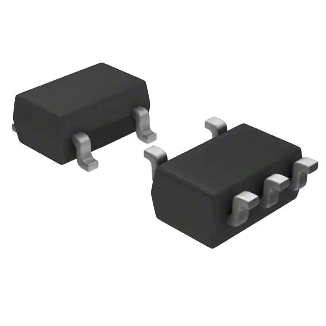
SOT23-5 Package (Top View)
Additional Information
Click these links for more information:
(Ti p )
1
NU
2
(Ring)
3
5
(Ti p )
PRODUCT TECHNICAL INVENTORY SAMPLES
SELECTOR LIBRARY
4
(Ring)
Terminal typical application names
shown in parenthesis.
NU - Non-usable; no external electrical
connection should be made to this terminal.
CONTACT
Agency Recognition
Description
UL
File Number: E215609
MD-SOT23-5-001-a
Device Symbol
Rated for International Surge Wave
Shapes
Wave
Shape
Standard
(Tip)
IPPSM
A
8/20
IEC 61000-4-5
30
10/1000
GR-1089-CORE
18
(Ring)
SD-TISP4-002-a
Description
This range of devices is designed to protect xDSL line-driver interfaces from overvoltages up to rated limits. Overvoltages are normally
caused by a.c. power-system or lightning-flash disturbances which are induced or conducted onto the telephone line. These symmetrical
protectors are two-terminal thyristor-crowbar devices. They can be used to protect between conductors, or a pair of devices can be
deployed to protect from line to ground.
When placed between the xDSL line driver IC and the transformer, this protector will clamp and switch into a low-impedance state, safely
diverting the energy transferred by the xDSL coupling transformer. The low capacitance design makes this device suitable for designs
from ADSL all the way up to 30 MHz VDSL2.
Telecom ports need protection against Common Mode (Longitudinal) and Differential (Metallic) surges, to comply with international
standards such as ITU-T K.20, K.21 or K.45, Telcordia GR-1089-CORE and YD/T. Common Mode surges are resisted by the galvanic
isolation of the coupling transformer which is commonly rated to 2 kV or greater. Differential surges can be transmitted by the transformer,
and can stress the Line Driver Interface IC. As the xDSL interface circuit is designed to operate from 3 kHz to to 30 MHz, nearby high
frequency events - such as cable flashover or primary protection activation - can generate damaging conditions for the interface requiring
this type of protection.
Please contact your Bourns representative if the protection voltage you require is not listed.
OCTOBER 2009 – REVISED JULY 2019
WARNING Cancer and Reproductive Harm
www.P65Warnings.ca.gov
*RoHS Directive 2015/863, Mar 31, 2015 and Annex.
Specifications are subject to change without notice.
Users should verify actual device performance in their specific applications.
The products described herein and this document are subject to specific legal disclaimers as set forth on the last page of
this document, and at www.bourns.com/docs/legal/disclaimer.pdf.
�TISP4P0xxL1N Overvoltage Protector Series
Absolute Maximum Ratings, TA = 25 °C (Unless Otherwise Noted)
Rating
‘4P015L1N
‘4P020L1N
‘4P025L1N
‘4P035L1N
Repetitive peak off-state voltag e
Symbol
Value
Unit
VDRM
±8
±12
±16
±24
V
Non-repetitive peak impulse curr ent (see Notes 1, 2 and 3)
8/20 μs (IEC 61000-4-5, 1.2/50 μs voltage, 8/20 current combinat ion wave generator)
10/1000 μs (GR-1089-CORE, 10/1000 μs voltage wave shape)
Junction temperatur e
Storage temperature range
IPPSM
±30
±18
A
TJ
-40 to +150
°C
Tstg
-65 to +150
°C
NOTES: 1. Initially the device must be in ther mal equilibrium with TJ = 25 °C.
2. The surge may be repeated after the device returns to its initial conditions .
3. Rated currents only apply if pins 1 & 5 (Tip) are connected together and pins 3 & 4 (Ring) are connected togethe r.
Electrical Characteristics, TA = 25 °C (Unless Otherwise Noted)
Parameter
IDRM
V(BO)
Test Conditions
Repetitive peak off-state curr ent
Breakover voltage
dv/dt = ±250 V/ms, RSOURCE = 300 Ω
IH
Holding current
CO
Off-state capacitance
ΔC
Delta-capacitance
Min
Typ
VD = VDRM
IT = ± 5 A, d i/ d t = ± 30 mA/ ms
f = 1 MHz, Vd = 1 V rms, VD = 2 V
f = 1 MHz, Vd = 1 V rms, VD = 1 V to VDRM
Typical Part Marking
‘4P015L1N
‘4P020L1N
‘4P025L1N
‘4P035L1N
‘4P015L1N
‘4P020L1N
‘4P025L1N
‘4P035L1N
‘4P015L1N
‘4P020L1N
‘4P025L1N
‘4P035L1N
‘4P015L1N
‘4P020L1N
‘4P025L1N
‘4P035L1N
± 30
±10
±30
±30
6.5
6
5.5
3.5
2
2.5
3
2
Max
Unit
±1
μA
±15
±20
±25
±35
V
mA
pF
pF
Environmental Specifications
2-DIGIT PRODUCT CODE
Y1 = TISP4P015L1NR
Y2 = TISP4P020L1NR
Y3 = TISP4P025L1NR
Y4 = TISP4P035L1NR
Moisture Sensitivity Level ................................................................. 1
ESD Classification (HBM)...............................................................3B
Y1YWWL
MANUFACTURING
DATE CODE:
Y = YEAR
WW = WEEK
L = LOT CODE
OCTOBER 2009 – REVISED JULY 2019
Specifications are subject to change without notice.
Users should verify actual device performance in their specific applications.
The products described herein and this document are subject to specific legal disclaimers as set forth on the last page of this document, and at www.bourns.com/docs/legal/disclaimer.pdf.
�TISP4P0xxL1N Overvoltage Protector Series
Parameter Measurement Information
+i
I PPSM
Quadrant I
Switching
Characteristic
ITSM
ITRM
IT
V(BO)
VT
I(BO)
IH
V(BR)M
VDRM
-v
I(BR)
V(BR)
I(BR)
IDRM
VD
ID
ID
VD
IDRM
+v
VDRM
V(BR)M
V(BR)
IH
I(BO)
VT
V(BO)
IT
ITRM
ITSM
Quadrant III
Switching
Characteristic
I PPSM
-i
PM-TISP4xxx-001-a
Figure 1. Voltage-Curr ent Characteristic for Tip and Ring Terminals
All Measurements are Referenced to the Ring Terminal
OCTOBER 2009 – REVISED JULY 2019
Specifications are subject to change without notice.
Users should verify actual device performance in their specific applications.
The products described herein and this document are subject to specific legal disclaimers as set forth on the last page of this document, and at www.bourns.com/docs/legal/disclaimer.pdf.
�TISP4P0xxL1N Overvoltage Protector Series
Typical Characteristics
CAPACITANCE
vs
OFF-STATE VOLTAGE
TC -4 PN -0 01
10
f = 1 MHz
Vd = 1 VRMS
TJ = 25 °C
9
8
Capacitance - pF
7
6
5
TISP4P015L1N
4
TISP4P020L1N
3
TISP4P025L1N
2
TISP4P035L1N
1
0
0
2
4
6
8
10 12 14 16 18 20 22 24
VD - Off-State Voltage - V
How to Order
Device
Package
Carrier
Order As
Reel Quantity
TISP4P0xxxL1N
SOT23-5
Embossed Tape Reeled
TISP4P0xxL1NR-S
10,000
Insert xx corresponding to device name.
Asia-Pacific: Tel: +886-2 2562-4117 • Email: asiacus@bourns.com
Europe: Tel: +36 88 885 877 • Email: eurocus@bourns.com
The Americas: Tel: +1-951 781-5500 • Email: americus@bourns.com
www.bourns.com
OCTOBER 2009 – REVISED JULY 2019
Specifications are subject to change without notice.
Users should verify actual device performance in their specific applications.
The products described herein and this document are subject to specific legal disclaimers as set forth on the last page of this document, and at www.bourns.com/docs/legal/disclaimer.pdf.
�TISP4P0xxL1N Overvoltage Protector Series
VDSL Application Examples
MF-RX018-250
TIP
+ tº
Tx
TISP4400M3
Rx
Ring
xDSL transceiver
TISP4P035L1N
Figure 3.
MF-RX018-250
TIP
+ tº
Tx
TISP4400M3
Rx
Ring
xDSL transceiver
TISP4P020L1N
Figure 4.
TIP
Tx
2035-35-SM
Rx
Ring
xDSL transceiver
CD143A-SR70
TISP4P035L1N
Figure 5.
Recommended PCB Layout
T
1
NU
2
R
3
5
T
PCB Track
4
R
PCB Track
MD-SOT223-5-xxx
Figure 6.
“TISP” is a trademark of Bourns, Ltd., a Bourns Company, and is registered in the U.S. Patent and Trademark Office.
“Bourns” is a registered trademark of Bourns, Inc. in the U.S. and other countries.
OCTOBER 2009 – REVISED JULY 2019
Specifications are subject to change without notice.
Users should verify actual device performance in their specific applications.
The products described herein and this document are subject to specific legal disclaimers as set forth on the last page of this document, and at www.bourns.com/docs/legal/disclaimer.pdf.
�Legal Disclaimer Notice
This legal disclaimer applies to purchasers and users of Bourns® products manufactured by or on behalf of Bourns, Inc. and
P[Z�HɉSPH[LZ��JVSSLJ[P]LS`��¸)V\YUZ¹��
Unless otherwise expressly indicated in writing, Bourns® products and data sheets relating thereto are subject to change
^P[OV\[�UV[PJL���
很抱歉,暂时无法提供与“TISP4P020L1NR-S”相匹配的价格&库存,您可以联系我们找货
免费人工找货- 国内价格 香港价格
- 10000+2.5041010000+0.32405
- 20000+2.3462420000+0.30362
- 30000+2.3185730000+0.30004
- 国内价格
- 1+9.46748
- 10+5.92429
- 100+3.90077
- 500+3.52694
- 国内价格 香港价格
- 1+11.214351+1.45120
- 10+7.0575710+0.91329
- 100+4.64680100+0.60132
- 500+3.61060500+0.46723
- 1000+3.276831000+0.42404
- 2000+2.995942000+0.38769
- 5000+2.837935000+0.36725