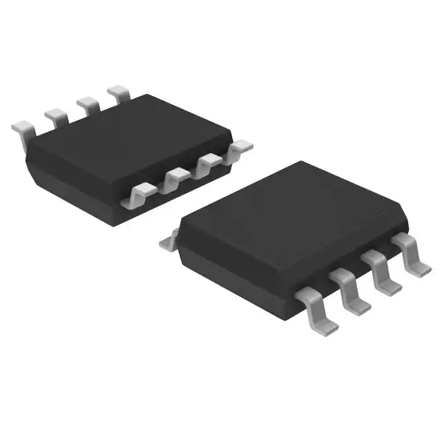
TISP83121D
DUAL-GATE UNIDIRECTIONAL OVERVOLTAGE PROTECTOR
TISP83121D Unidirectional P & N-Gate Protector
Overvoltage Protection for Dual-Voltage Ringing SLICs
– Programmable Protection Configurations up to ±100 V
– Typically 5 Lines Protected by:
Two TISP83121D + Diode Steering Networks
Additional Information
Click these links for
more information:
PRODUCT TECHNICAL INVENTORY SAMPLES
SELECTOR LIBRARY
High Surge Current
– 150 A, 10/1000 μs
– 250 A, 10/700 μs
– 500 A, 8/20 μs
CONTACT
Agency Recognition
Pin Compatible with the LCP3121
– 50 % more surge current
– Functional Replacement in Diode Steering Applications
Description
UL
File Number: E215609
Small Outline Surface Mount Package
8-SOIC Package (Top View)
Description
The TISP83121D is a dual-gate reverse-blocking unidirectional
thyristor designed for the protection of dual-voltage ringing SLICs
(Subscriber Line Interface Circuits) against overvoltages on
the telephone line caused by lightning, a.c. power contact and
induction.
K
1
8
K
G1
2
7
A
G2
3
6
A
K
4
5
K
MD6XAYB
The device chip is a four-layer NPNP silicon thyristor structure
which has an electrode connection to every layer. For negative
overvoltage protection the TISP83121D is used in a common anode
configuration with the voltage to be limited applied to the cathode
(K) terminal and the negative reference potential applied to the gate
1 (G1) terminal. For positive overvoltage protection the TISP83121D
is used in a common cathode configuration with the voltage to be
limited applied to the anode (A) terminal and the positive reference
potential applied to the gate 2 (G2) terminal.
For operation at the rated current values connect pins 1, 4, 5 and 8
together.
Device Symbol
A
G2
The TISP83121D is a unidirectional protector and to prevent reverse
bias, requires the use of a series diode between the protected line
conductor and the protector. Further, the gate reference supply
voltage requires an appropriately poled series diode to prevent the
supply from being shorted when the TISP83121D crowbars.
Under low level power cross conditions the TISP83121D gate
current will charge the gate reference supply. If the reference
supply cannot absorb the charging current its potential will increase,
possibly to damaging levels. To avoid excessive voltage levels a
clamp (zener or avalanche breakdown diode) may be added in
shunt with the supply. Alternatively, a grounded collector emitterfollower may be used to reduce the charging current by the
transistor’s HFE value.
G1
K
SD6XAKA
................................................... UL Recognized Component
This monolithic protection device is made with an ion-implanted
epitaxial-planar technology to give a consistent protection
performance and be virtually transparent to the system in normal
operation.
FEBRUARY 1999 – REVISED JULY 2019
WARNING Cancer and Reproductive Harm
www.P65Warnings.ca.gov
*RoHS Directive 2015/863, Mar 31, 2015 and Annex.
Specifications are subject to change without notice.
Users should verify actual device performance in their specific applications.
The products described herein and this document are subject to specific legal disclaimers as set forth on the last page of
this document, and at www.bourns.com/docs/legal/disclaimer.pdf.
�TISP83121D Unidirectional P & N-Gate Protector
How To Order
Device
Package
Order As
Carrier
TISP83121 D (8-pin Small-Outline) R (Embossed Tape Reeled)
TISP83121DR-S
Absolute Maximum Ratings
Rating
Repetitive peak off-state voltage, 0 °C to 70 °C
Symbol
Value
Unit
VDRM
100
V
Non-repetitive peak on-state pulse current (see Notes 1 and 2)
10/1000 μs (GR-1089-CORE, open-circuit voltage wave shape 10/1000 μs)
150
ITSP
5/310 μs (CCITT K20/21, open-circuit voltage wave shape 7 kV, 10/700 μs)
A
250
8/20 μs (ANSI C62.41, open-circuit voltage wave shape 1.2/50 μs)
500
Non-repetitive peak on-state current, 50 Hz, halfwave rectified sinewave, (see Notes 1 and 2)
22
100 ms
1s
8
ITSM
A
3
900 s
Junction temperature
Storage temperature range
TJ
-40 to +150
°C
Tstg
-65 to +150
°C
NOTES: 1. Initially the protector must be in thermal equilibrium with 0 °C < TJ < 70 °C. The surge may be repeated after the device returns to
its initial conditions. For operation at the rated current value, pins 1, 4, 5 and 8 must be connected together.
2. Above 70 °C, derate linearly to zero at 150 °C lead temperature.
Electrical Characteristics, TJ = 25 °C (Unless Otherwise Noted)
Parameter
ID
IDRM
Off-state current
Repetitive peak offstate current
Test Conditions
Min
Vd = 70 V, IG = 0
Vd = VDRM = 100 V, IG = 0, 0 °C to 70 °C
Holding current
IR
Reverse current
IT = 1 A, di/dt = -1A/ms
VR = 0.3 V
Max
Unit
1
μA
10
μA
300
TJ = 0 to 70 °C
IH
Typ
TJ = 25 °C
90
TJ = 70 °C
60
mA
1
mA
IG1T
Gate G1 trigger current IT = +1 A, t p(g) = 20 μs
+200
mA
IG2T
Gate G2 trigger current IT = +1 A, t p(g) = 20 μs
-180
mA
VG1T
G1-K trigger voltage
IT = +1 A, t p(g) = 20 μs
+1.8
V
VG2T
G2-A trigger voltage
IT = +1 A, t p(g) = 20 μs
-1.8
V
f = 1 MHz, Vd = 1 V rms, VD = 5 V, IG = 0 (see Note 3)
100
pF
CAK
NOTE
Anode-cathode offstate capacitance
3: These capacitance measurements employ a three terminal capacitance bridge incorporating a guard circuit. The unmeasured
device terminals are a.c. connected to the guard terminal of the bridge.
FEBRUARY 1999 – REVISED JULY 2019
Specifications are subject to change without notice.
Users should verify actual device performance in their specific applications.
The products described herein and this document are subject to specific legal disclaimers as set forth on the last page of this document, and at www.bourns.com/docs/legal/disclaimer.pdf.
�TISP83121D Unidirectional P & N-Gate Protector
Thermal Characteristics
Parameter
R θJA
Test Conditions
Junction to free air thermal resistance
Min
TA = 25 °C, EIA/JESD51-3 PCB,
EIA/JESD51-2 environment, IT = ITSM(900)
Typ
Max
Unit
105
°C/W
Parameter Measurement Information
+i
QUADRANT I
ANODE POSITIVE
SWITCHING CHARACTERISTIC
VGT
IH
VR
ID
-v
VDRM
IR
QUADRANT III
ANODE NEGATIVE
REVERSE CHARACTERISTIC -i
REFERENCE
VOLTAGE
+v
PM6XAGB
Figure 1. Voltage-Current Characteristic
Asia-Pacific: Tel: +886-2 2562-4117 • Email: asiacus@bourns.com
EMEA: Tel: +36 88 885 877 • Email: eurocus@bourns.com
The Americas: Tel: +1-951 781-5500 • Email: americus@bourns.com
www.bourns.com
“TISP” is a trademark of Bourns, Ltd., a Bourns Company, and is Registered in the U.S. Patent and Trademark Office.
“Bourns” is a registered trademark of Bourns, Inc. in the U.S. and other countries.
FEBRUARY 1999 – REVISED JULY 2019
Specifications are subject to change without notice.
Users should verify actual device performance in their specific applications.
The products described herein and this document are subject to specific legal disclaimers as set forth on the last page of this document, and at www.bourns.com/docs/legal/disclaimer.pdf.
�Legal Disclaimer Notice
This legal disclaimer applies to purchasers and users of Bourns® products manufactured by or on behalf of Bourns, Inc. and
P[Z�HɉSPH[LZ��JVSSLJ[P]LS`��¸)V\YUZ¹��
Unless otherwise expressly indicated in writing, Bourns® products and data sheets relating thereto are subject to change
^P[OV\[�UV[PJL���