3584
®
High Voltage, High Speed
OPERATIONAL AMPLIFIER
FEATURES
APPLICATIONS
● WIDE POWER SUPPLY VOLTAGE:
±70V to ±150V
● GAIN-BANDWIDTH PRODUCT: 50MHz
● SLEW RATE: 150V/µs
● FET INPUT: IB = 20pA max
● THERMAL SHUT-DOWN PROTECTION
● PROGRAMABLE POWER SUPPLY
● PIEZO-ELECTRIC TRANSDUCER DRIVER
● ELECTROSTATIC TRANSDUCER DRIVER
● CRT DEFLECTION
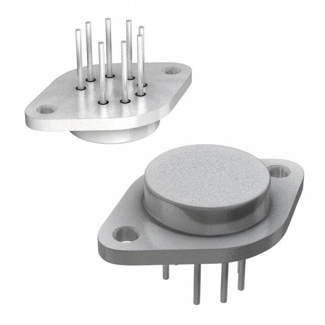
● HERMETIC TO-3 PACKAGE, ISOLATED
CASE
DESCRIPTION
Offset Trim
3
4
Compensation
8
V+
2
The 3584 is a high voltage, high speed hybrid operational amplifier designed for a wide variety of
programmable power supply and transducer driver
applications.
The 3584 operates over a wide power supply range
(±70V to ±150V) and provides outputs up to 15mA.
Laser-trimmed FET input circuitry provides low offset
voltage (3mV max) and low input bias current (20pA
max). Thermal shut-down circuitry protects internal
circuitry from excessive power dissipation.
The 3584 provides a gain-bandwidth product of 20MHz
min (50MHz typical). External frequency compensation (series R/C) allows the user to optimize the
bandwidth and slew rate for a particular application.
5
–In
1
Output
6
+In
Specified temperature range is 0°C to +70°C. The
3584’s hermetic 8-pin TO-3 package is electrically
isolated from all internal circuitry.
International Airport Industrial Park • Mailing Address: PO Box 11400
Tel: (520) 746-1111 • Twx: 910-952-1111 • Cable: BBRCORP •
©
SBOS131
1978 Burr-Brown Corporation
7
V–
• Tucson, AZ 85734 • Street Address: 6730 S. Tucson Blvd. • Tucson, AZ 85706
Telex: 066-6491 • FAX: (520) 889-1510 • Immediate Product Info: (800) 548-6132
PDS-376B
Printed in U.S.A. October, 1993
�SPECIFICATIONS
ELECTRICAL
TCASE = +25°C, VS = ±150V, unless otherwise noted.
3584JM
PARAMETER
CONDITIONS
OFFSET VOLTAGE
Input Offset Voltage
vs Temperature
vs Power Supply
vs Time
INPUT BIAS CURRENT(1)
Input Bias Current
vs Temperature
vs Power Supply
Input Offset Current
vs Temperature
vs Power Supply
MIN
Specified Temperature Range
VCM = 0V
FREQUENCY RESPONSE
Unity-Gain Bandwidth
Gain-Bandwidth Product
Full-Power Bandwidth
Slew Rate
Settling Time: 0.1%
VCM = 0V
Linear Operation
No Load, DC
Rated Load, DC
±3
±25
mV
µV/°C
µV/V
µV/month
–20
pA
±20
pA/V
pA
Doubles Every 10°C
0.2
pA/V
5
1.7
0.3
µVp-p
µVrms
pAp-p
(V+) + |V–|
V– to V+
VS – 10
110
V
dB
1011||10
1011
Ω || pF
Ω || pF
120
dB
dB
7
135
150
12
MHz
MHz
kHz
V/µs
µs
±25
10
V
mA
mA
nF
100
Small-Signal
f = 1kHz, G = 100
G = 100
G = 100
G = 100
20
OUTPUT
Voltage Output
Current Output
Short Circuit Current
Load Capacitance (Maximum)
POWER SUPPLY
Operating Voltage Range
Quiescent Current
UNITS
Doubles Every 10°C
0.2
INPUT IMPEDANCE
Differential
Common-Mode
OPEN-LOOP GAIN
Open-Loop Voltage Gain
Open-Loop Voltage Gain
MAX
20
50
NOISE
Voltage, 0.01Hz to 10Hz
10Hz to 1kHz
Current, 0.01Hz to 10Hz
INPUT VOLTAGE RANGE
Maximum Safe Differential Input
Maximum Safe Common-Mode Input
Common-Mode Input Range
Common-Mode Rejection
TYP
VS - 5
±15
±70
±150
±6.5
V
mA
0
–55
–55
+70
+125
+150
°C
°C
°C
IO = 0
TEMPERATURE RANGE
Specification
Operating
Storage
NOTE: (1) Inputs may be damaged by input slew rates exceeding 1000V/µs. Inputs can be protected from signals exceeding 1000V/µs by limiting input current to 150mA
with external series resistors (pins 5 and 6).
The information provided herein is believed to be reliable; however, BURR-BROWN assumes no responsibility for inaccuracies or omissions. BURR-BROWN
assumes no responsibility for the use of this information, and all use of such information shall be entirely at the user’s own risk. Prices and specifications are subject
to change without notice. No patent rights or licenses to any of the circuits described herein are implied or granted to any third party. BURR-BROWN does not
authorize or warrant any BURR-BROWN product for use in life support devices and/or systems.
®
3584
2
�CONNECTION DIAGRAM
ORDERING INFORMATION
MODEL
PACKAGE
TEMPERATURE
RANGE
3584JM
8-Pin TO-3
0°C to +70°C
Top View
Optional
Offset
Adjust
Offset
Trim
2
3
100kΩ
+VCC
1
to +VCC
PACKAGE INFORMATION
Output
4
Offset
Trim
5
–In
8
7
RC
–VCC
CC
6
+In
Compensation
MODEL
PACKAGE
PACKAGE DRAWING
NUMBER(1)
3584JM
8-Pin TO-3
030
NOTE: (1) For detailed drawing and dimension table, please see end of data
sheet, or Appendix D of Burr-Brown IC Data Book.
Optional Socket: Burr-Brown Model 0804MC
TYPICAL PERFORMANCE CURVES
TCASE = +25°C, VS = ±150V, unless otherwise noted.
OUTPUT VOLTAGE vs FREQUENCY
SLEW RATE vs SUPPLY VOLTAGE AT FULL LOAD
1.0
Compensation:
200Ω and 0.1µF
2kΩ and 500pF
20Ω and 50pF
120
Normalized Slew Rate
Output Voltage (±Vp-p)
150
90
60
Compensation: 200Ω and 0.01µF
0.9
0.8
25°C to 85°C (Case)
0.7
–25°C (Case)
0.6
30
0.5
0
10k
100k
1M
40
10M
50
60
70
80
90
100
Power Supply (% of max)
Frequency (Hz)
OPEN-LOOP FREQUENCY RESPONSE FULL LOAD
SLEW RATE vs COMPENSATION
120
160
100
Voltage Gain (dB)
Slew Rate (V/µs)
120
80
40
80
60
Compensation:
200Ω and 0.1µF
2kΩ and 500pF
20Ω and 50pF
40
20
0
–20
0
200
2k
1
20k
10
100
1k
10k
100k
1M
10M
Frequency (Hz)
External Compensation Impedance (Ω)
®
3
3584
�TYPICAL PERFORMANCE CURVES (CONT)
TCASE = +25°C, VS = ±150V, unless otherwise noted.
OPEN-LOOP GAIN
vs SUPPLY VOLTAGE AT MAX LOAD
POWER DISSIPATION
5
–1
Internal Power Dissipation (W)
∆ Open-Loop Gain (dB)
0
25°C (Case)
–2
–3
–25°C (Case)
+85°C (Case)
–4
–5
–6
Case
4
θJC = 12°C/W
3
Ambient
2
θJA = 42°C/W
1
0
40
60
50
70
80
90
100
0
25
50
Power Supply (% of max)
Total Input Noise (µVp-p, µVrms)
20
Output Current
DC
10
Internal Current Limit
0
–10
DC
–20
5ms
–30
–50
–100
0
50
100
(rms) 10Hz to 10kHz
100
(p-p) 0.01Hz to 10kHz
(rms) 10Hz to 1kHz
10
1
Noise of Source Resistor
Amplifier Noise
0
103
150
104
Output Voltage
CURRENT LIMIT vs TEMPERATURE
106
107
108
COMMON-MODE REJECTION
120
10
100
0
80
CMR (dB)
Normalized Current Limit (%)
105
Source Resistance (Ω)
20
–10
Compensation: 200Ω and 0.01µF
60
–20
40
–30
20
0
–40
–50
125
1000
5ms
–150
100
NOISE vs SOURCE RESISTANCE
SAFETY OPERATING AREA (Secondary Breakdown)
30
75
Temperature (°C)
–25
0
25
50
75
100
125
1
®
3584
10
100
1k
Frequency (Hz)
Case Temperature (°C)
4
10k
100k
1M
�TYPICAL PERFORMANCE CURVES (CONT)
TCASE = +25°C, VS = ±150V, unless otherwise noted.
MAXIMUM COMMON-MODE VOLTAGE
vs FREQUENCY
POWER SUPPLY REJECTION vsFREQUENCY
120
150
Power Supply Rejection (dB)
Common-Mode Voltage (±)
Compensation: 200Ω and 0.01µF
125
100
75
50
25
100
80
60
Positive Supply
40
Negative Supply
20
0
0
10k
100k
10
1M
100
1k
Frequency (Hz)
10k
100k
1M
Frequency (Hz)
APPLICATION INFORMATION
Figure 1 shows the basic connections required to operate the
3584. Bypass capacitors should be connected close to the
device pins. Be sure that these capacitors have an adequate
voltage rating.
The thermal shut-down circuit will normally protect the
amplifier during a short-circuit to ground. It will not protect
against short-circuit to one of the power supplies. The
typical performance curve “Safe Operating Area” shows that
the large stress occurring during this high voltage condition
may cause damage if it exceeds 5ms duration. The thermal
protection circuitry will not activate fast enough to protect
the device from short-circuits to one of the power supplies.
Frequency compensation components must be connected to
pin 8 for closed-loop gains of 100 or less. Recommended
values are shown in Figure 1. Some adjustment in these
values may be required depending on exact circuit configuration and load conditions. Be sure the compensation capacitor has a voltage rating equal to or greater than the positive
power supply voltage, V+. Standard 0.25W resistors can be
used for RC.
The package case of the 3584 is electrically isolated from all
circuitry. No special insulating hardware is required. Although not absolutely required, it is recommended that the
case be connected to ground.
Input offset voltage and drift of the 3584 are laser-trimmed.
Many applications require no external offset trimming.
Figure 1 shows connection of an optional offset trim potentiometer which connects to pins 3 and 4.
V+
FET input circuitry reduces the input bias current of the
3584 to less than 20pA at room temperature. Input bias
current remains nearly constant throughout the full common-mode range. Input bias current approximately doubles
for each 10°C increase in case temperature above 25°C.
Heat sinking can help minimize this effect by reducing the
case temperature.
+70V to +150V
V+
100kΩ
4
3
3584
0.1µF
R1
R2
G=1+
Input circuitry of the 3584 is protected with series limiting
resistors and input clamp diodes. The inputs can withstand
the full rated supply voltage of ±150V (common-mode or
differential).
5
VIN
Connect case
to ground.
THERMAL PROTECTION
The 3584 has internal thermal shut-down circuitry that
activates at a case temperature of approximately 150°C or
higher. As this circuitry is activated, the output current drive
is reduced. As the case temperature returns to less than the
activation temperature, operation will return to normal.
Optional offset
voltage trim
circuit.
6
R2
R1
2
3584
7
1
8
RC
0.1µF
CC
V–
–70V to –150V
VO
Gain
1
10
100
1000
CC
RC
10nF
200Ω
500pF
2kΩ
50pF
20kΩ
(no connection)
Interpolate values for
intermediate gains.
FIGURE 1. Basic Circuit Connections.
®
5
3584
�PACKAGE OPTION ADDENDUM
www.ti.com
17-Oct-2003
PACKAGING INFORMATION
ORDERABLE DEVICE
STATUS(1)
PACKAGE TYPE
PACKAGE DRAWING
PINS
PACKAGE QTY
3584JM
NRND
TO/SOT
LMF
8
1
(1) The marketing status values are defined as follows:
ACTIVE: Product device recommended for new designs.
LIFEBUY: TI has announced that the device will be discontinued, and a lifetime-buy period is in effect.
NRND: Not recommended for new designs. Device is in production to support existing customers, but TI does not recommend using this part in
a new design.
PREVIEW: Device has been announced but is not in production. Samples may or may not be available.
OBSOLETE: TI has discontinued the production of the device.
�IMPORTANT NOTICE
Texas Instruments Incorporated and its subsidiaries (TI) reserve the right to make corrections, modifications,
enhancements, improvements, and other changes to its products and services at any time and to discontinue
any product or service without notice. Customers should obtain the latest relevant information before placing
orders and should verify that such information is current and complete. All products are sold subject to TI’s terms
and conditions of sale supplied at the time of order acknowledgment.
TI warrants performance of its hardware products to the specifications applicable at the time of sale in
accordance with TI’s standard warranty. Testing and other quality control techniques are used to the extent TI
deems necessary to support this warranty. Except where mandated by government requirements, testing of all
parameters of each product is not necessarily performed.
TI assumes no liability for applications assistance or customer product design. Customers are responsible for
their products and applications using TI components. To minimize the risks associated with customer products
and applications, customers should provide adequate design and operating safeguards.
TI does not warrant or represent that any license, either express or implied, is granted under any TI patent right,
copyright, mask work right, or other TI intellectual property right relating to any combination, machine, or process
in which TI products or services are used. Information published by TI regarding third-party products or services
does not constitute a license from TI to use such products or services or a warranty or endorsement thereof.
Use of such information may require a license from a third party under the patents or other intellectual property
of the third party, or a license from TI under the patents or other intellectual property of TI.
Reproduction of information in TI data books or data sheets is permissible only if reproduction is without
alteration and is accompanied by all associated warranties, conditions, limitations, and notices. Reproduction
of this information with alteration is an unfair and deceptive business practice. TI is not responsible or liable for
such altered documentation.
Resale of TI products or services with statements different from or beyond the parameters stated by TI for that
product or service voids all express and any implied warranties for the associated TI product or service and
is an unfair and deceptive business practice. TI is not responsible or liable for any such statements.
Following are URLs where you can obtain information on other Texas Instruments products and application
solutions:
Products
Amplifiers
Applications
amplifier.ti.com
Audio
www.ti.com/audio
Data Converters
dataconverter.ti.com
Automotive
www.ti.com/automotive
DSP
dsp.ti.com
Broadband
www.ti.com/broadband
Interface
interface.ti.com
Digital Control
www.ti.com/digitalcontrol
Logic
logic.ti.com
Military
www.ti.com/military
Power Mgmt
power.ti.com
Optical Networking
www.ti.com/opticalnetwork
Microcontrollers
microcontroller.ti.com
Security
www.ti.com/security
Telephony
www.ti.com/telephony
Video & Imaging
www.ti.com/video
Wireless
www.ti.com/wireless
Mailing Address:
Texas Instruments
Post Office Box 655303 Dallas, Texas 75265
Copyright 2003, Texas Instruments Incorporated
�