®
4127
LOGARITHMIC AMPLIFIER
FEATURES
current and four decades of input voltage. In addition,
a current inverter and a precise internal reference
allow pin programming of the 4127 as a logarithmic,
log ratio, or antilog amplifier.
● ACCEPTS INPUT VOLTAGES OR
CURRENTS OF EITHER POLARITY
● WIDE INPUT DYNAMIC RANGE
6 Decades of Current
4 Decades of Voltage
To further increase its versatility and reduce your
system cost, the 4127 has an uncommitted operational
amplifier in its package that can be used as a buffer,
inverter, filter, or gain element.
● VERSATILE
Log, Antilog, and Log Ratio Capability
The 4127 is available with initial accuracies (log
conformity) of 0.5% and 1.0%, and operates over an
ambient temperature range of –10°C to +70°C.
DESCRIPTION
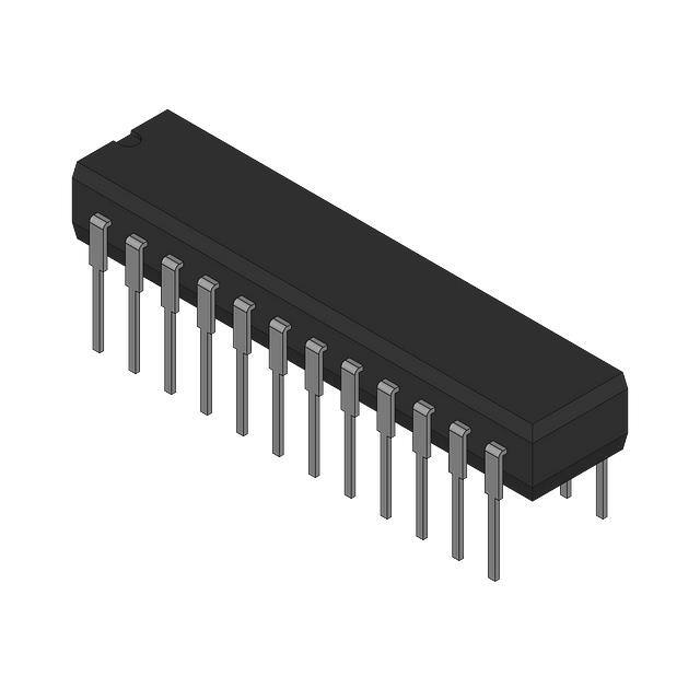
Packaged in a ceramic double wide DIP, the 4127 is
the first hybrid logarithmic amplifier that accepts
signals of either polarity from current or voltage
sources. A special purpose monolithic chip, developed specifically for logarithmic conversions,
functions accurately for up to six decades of input
With its versatility and high performance, the 4127
has many applications in signal compression, transducer linearization, and phototube buffering.
Manufacturers of medical equipment, analytical
instruments, and process control instrumentation will
find the 4127 a low cost solution to many signal
processing problems.
+15VDC
–15VDC
International Airport Industrial Park • Mailing Address: PO Box 11400
Tel: (520) 746-1111 • Twx: 910-952-1111 • Cable: BBRCORP •
©
SBFS010
1976 Burr-Brown Corporation
• Tucson, AZ 85734 • Street Address: 6730 S. Tucson Blvd. • Tucson, AZ 85706
Telex: 066-6491 • FAX: (520) 889-1510 • Immediate Product Info: (800) 548-6132
PDS-346F
Printed in U.S.A. October, 1993
�SPECIFICATIONS
PIN CONFIGURATION
Top View
ELECTRICAL
Typical Specifications at +25°C with rated supplies, unless otherwise noted.
MODEL
ACCURACY(1), % of FSR
Current Source Input: 1nA to 1mA
Voltage Input: 1mV to 10V
INPUT
Current Source Input, Pin 4
Current Source Input, Pin 7
Reference Current Input, Pin 2
Absolute Maximum Inputs
4127KG
4127JG
0.5% max
0.5% max
1% max
1% max
STABILITY
Scale Factor Drift (∆A/°C)
Reference Current Drift (∆IR/°C)
Input Offset Current Drift (∆IS/°C)
Input Offset Voltage Drift
Accuracy vs Supply Variation
Reference Current
Input Offset Voltage
Input Noise - Current Input
Input Noise - Voltage Input
POWER SUPPLY REQUIREMENTS
Rated Supply Voltages
Supply Voltage Range
Supply Current Drain
at Quiescent, max
at Full Load, max
IREF Input
2
23 IREFBias
No Pin Present
3
22 Postive Supply
(1)
4
21 Common
(1)
5
20 No Pin Present
No Pin Present
6
19 Gain Adjust
Current Inverter Input
7
18 Log Output
No Pin Present
8
17 No Pin Present
Op Amp + Input
9
16 No Pin Present
90kHz
50kHz
5kHz
250Hz
80Hz
Op Amp –Input 10
15 No Pin Present
Op Amp Output 11
14 Negative Supply
No Pin Present 12
13 NC
NOTE: (1) Pins 4 and 5 are internally connected.
10ms
±0.0005A/°C
±0.001 I R/°C for IR ≥ 1µA
±0.003 IR/°C for 400nA < IR < 1µA
10pA at +25°C, Doubles Every 10°C
±10µV/°C
PACKAGE INFORMATION
±0.001IR/V
±300µV/V
1pA, rms, 10Hz to 10kHz
10µA, rms, 10Hz to 10kHz
UNCOMMITTED OP AMP CHARACTERISTICS
Input Offset Voltage
Input Bias Current
Input Impedance
Large Signal Voltage Gain
Output Current
TEMPERATURE RANGE
Specification
Operating
Storage
24 No Pin Present
Current Inverter Output
±10V
±5mA
10Ω
FREQUENCY RESPONSE
–3dB Small Signal at Current Input
of 100µA
of 10µA
of 1µA
of 100nA
of 10nA
Step Response to within ±1% of
Final Value (IR = 1µA, A = 5)
1
+I Input
+1nA to +1mA
–1nA to –1mA
+1µA to +1mA
±10mA or ±Supply Volts
OUTPUT
Voltage
Current
Impedance
IREF Output
MODEL
PACKAGE
PACKAGE DRAWING
NUMBER(1)
4127KG
4127JG
24-Pin
24-Pin
075
075
NOTE: (1) For detailed drawing and dimension table, please see end of data
sheet, or Appendix D of Burr-Brown IC Data Book.
5mV
40nA
1MΩ
85dB
5mA
0°C to +60°C
–10°C to +70°C
–55°C to +125°C
±15VDC
±14VDC to ±16VDC
±20mA
±26mA
NOTE: (1) Log conformity at 25°C.
The information provided herein is believed to be reliable; however, BURR-BROWN assumes no responsibility for inaccuracies or omissions. BURR-BROWN
assumes no responsibility for the use of this information, and all use of such information shall be entirely at the user’s own risk. Prices and specifications are subject
to change without notice. No patent rights or licenses to any of the circuits described herein are implied or granted to any third party. BURR-BROWN does not
authorize or warrant any BURR-BROWN product for use in life support devices and/or systems.
®
4127
2
�TYPICAL PERFORMANCE CURVES
At +25°C with rated supplies, unless otherwise noted.
RELATIONSHIP OF SCALE FACTOR “A”
TO GAIN SETTING RESISTOR, R2
RELATIONSHIP OF REFERENCE CURRENT, IR
AND EXTERNAL RESISTOR, R1
10
100µA
9
Scale Factor “A” (V)
Reference Current
8
10µA
1µA
100nA
EO = –A log10
7
6
5
4
3
2
IS
IR
1
EO = –A log10
0
10nA
10k
100k
1M
10M
0
100M
20
|IS|
AND OUTPUT
IR
VOLTAGE IN TERMS OF “A”
EO = –A log10
EO – Volts
10
IR
0.001 0.01 0.1
IR
IR IR
IR
80
RELATIONSHIP OF
Output
Voltage
|IS|
IR
10V
Input
Current
IS
2A
60
|IS|
AND OUTPUT VOLTAGE
IR
For IR = 1µA and A = 5V and 10V
LOG RELATIONSHIP OF
4A
IR
Resistance (kΩ)
Resistance (Ω)
Output
Voltage
40
|IS|
EO = –A log
Input
Current
IS
A = 5V
0.01µA 0.1µA
1µA
–5V
–2A
–10V
–4A
IR
A = 10V
5V
100 1000
IR
IR
|IS|
10µA
100µA
Range of
Adjustment
40dB
80dB
DISCUSSION OF
SPECIFICATIONS
ACCURACY
The deviation from the ideal output voltage defined as a
percent of the full scale output voltage.
INPUT/OUTPUT RANGE
The log relationships of –A log
IS
IR
and –A log
ES
IRR
STABILITY
The use of a monolithic transistor quad and low-drift amps
minimizes drift, but some drift remains in the scale-factor,
reference current, and input offset. Input offset consists of a
bias current plus the op amp input voltage offset divided by
the signal source resistance. Also, there is some slight drift
in conformity to the log function and in output amplifier
offset, but this is generally negligible.
are
subject to the constraints specified. The 4127 can be operated with inputs lower than those given, but the accuracy
will be degraded.
THEORY OF OPERATION
The 4127 is a complete logarithmic amplifier that can be
pin-programmed to accept input currents or voltages of
either polarity. By making use of the internal current inverter, reference current generator, log ratio element, and
uncommitted op amp, you can generate a variety of logarith-
FREQUENCY RESPONSE
The small-signal frequency response varies considerably
with signal level and scaling, so the frequency response is
specified under several different operating conditions.
®
3
4127
�From the semiconductor junction characteristics, the baseto-emitter voltage will be:
mic functions, including the log ratio of two signals, the
logarithm of an input signal, or the antilog of an input signal.
The unique FET-input current-inverting element removes
the polarity limitations present in most conventional log
amplifiers.
VBE ≈
Utilizing the inherent exponential characteristics of transistor functions, the 4127 calculates accurate log functions for
input currents from 1nA to 1mA, or input voltages from
1mV to 10V. Carefully matched monolithic quad transistors
and temperature sensitive gain elements are used to produce
a log amplifier with excellent temperature characteristics.
IL
,
where: IC = Collector current
IL = Reverse saturation current
q, m, K = Constants
T = Absolute temperature
So E1 = –
A functional diagram of the 4127 circuit is shown in
Figure 1. In addition to the basic log amplifier, the 4127
contains a separate internal current source, a current
inverter, and an uncommitted operational amplifier. The
current inverter accurately converts negative input current to
a positive current of equal magnitude.
IS
IR
mKT1
mKT2
ln
and E2 – E1 =
ln
q
IL1
q
IL2
If the transistors Q1 and Q2 are at the same temperature and
have matched characteristics, then:
The 4127 is capable of accurately logging input current over
a 120dB range, but to use this full range, good shielding
practice must be followed. A current source input is, by
definition, a high impedance source and is therefore subject
to electrostatic pickup.
E2 =
mKT
q
E2 =
–mKT
ln
q
ln
IR
IL
– ln
IS
IL
IS
IR
The output op amp, A2, provides a voltage gain of approximately (RT + R2)/RT, and the value of (mKT)/q is about
26mV at room temperature. Since resistor RT varies with
temperature to compensate for gain drift, the output voltage,
EO, expressed as a log will be:
The input op amps, A1 and A3, have FET input stages for low
noise and very-low input bias current. The op amp, A1, will
make the collector current of Q1 equal to the signal input
current IS, and the collector current of Q2 will be the
reference input current IR.
Current
Inverter
Input
IC
mKT
ln
q
RT
Gain
19 Adjust
≈520Ω Thermistor
IS
7
R2
A3
Current
Inverter
Output
Q2
IS
E2
A2
EO
Gain
18
Log Output
10
5
Op Amp
–Input
Q1
+IINPUT I
S
A4
4
A1
E1
11 Op Amp
Output
9
Op Amp
+Input
IREF
Input IR
2
5kΩ
23
IR
1
IREF
Output
–15VDC
IREF
IR
22
R1
+15VDC
+15VDC
14
–15VDC
21
FIGURE 1. Functional Diagram.
®
4127
4
Common
�IS
EO = –A log10
where A ≈
RT + R2
RT
IR
IMAX
,
IR
1
(26mV)
0.434
IS
1µA
CONNECTION DIAGRAMS
Transfer function is EO = –A log
I1
where I1 is a positive
IR
input current and IR is the resistor-programmed internal
reference current (see Figure 2).
CHOOSING THE OPTIMUM
SCALE FACTOR AND REFERENCE CURRENT
To minimize the effects of output offset and noise, it is
usually best to use the full ±10V output range. Once an
output range of ±10V has been chosen, then “A” and IR can
be determined from the Min/Max of the input current, IS.
+15VDC
Reference
Current
–15VDC
22
21
14
23
18
4
IS
, where IMIN < IS < IMAX
IR
I1
EO
Gain
R2
4127
19
1
2
(1)
R3
The output range of ±10V for an input range of IMIN to IMAX
means that:
NOTE: (1) Needed only
if I1< 10nA.
+15VDC
IMIN
IR
and –10 = – A log
IMAX
IR
IMAX + IMIN
IR2
= 0, or IR = IMAX IMIN
2. Apply |I1| = IR, adjust R1 such that EO = 0.
3. Apply |I1| = IMAX, adjust R2 for the proper output voltage.
IMAX
4. Repeat steps 2 and 3 if necessary.
IMAX IMIN
5. Ignore this step if |I1MIN| ≥ 10nA. Otherwise, apply |I1| =
1nA, make R3 = 1kMΩ and adjust R4 for the proper
output voltage. For R3, a single resistor is recommended.
A voltage divider network is difficult to use due to
amplifier offset voltage.
In terms of the input current range for IS, the values for IR and
A that will provide a full ±10V output swing are:
IR = IMAX IMIN and A =
log
–15VDC
ADJUSTMENT PROCEDURE
1. Refer to Choosing the Optimum Scale Factor and
Reference Current.
The value for A can be found from:
10 = A log
R4(1)
10kΩ
FIGURE 2. Transfer Function When I1 is Positive.
Adding these two equations together
log
= 2; So, A = 5
EO = –5log
The relationship between the input current, IS, and the output
voltage, EO, in terms of the externally adjusted parameters,
IR and “A”, is illustrated in Typical Performance Curves.
This relationship is, of course, restricted to values of IS
between 1nA and 1mA and output voltages of less than
±10V.
+10 = –A log
IR
10–4
= 100
10–6
For an IR of 1µA and A of 5,
The external resistor R1 sets the reference current IR and
resistor R2 sets the scale-factor “A”. R1 and R2 must be
trimmed to the desired values, but the approximate relationships are shown in Typical Performance Curves.
EO = – A log
IMAX
log
, RT ≈ 520Ω
=
10
IMAX
IR
Transfer function is EO = –A log
EXAMPLE
|I1|
IR
where I1 is a negative
input current and IR is the resistor-programmed internal
reference current (see Figure 3).
Assume that IMIN is +10nA and IMAX is +100µA.
This is an 80dB range.
IR = IMAX IMIN =
(10–4) (10–8) = 10–6, or 1µA.
®
5
4127
�+15VDC
4. Apply E1 = EMIN, adjust R3 for the proper output.
–15VDC
5. Repeat steps 2 through 4 if necessary.
Reference
Current
22
21
14
23
EO
18
4127
7
I1
Transfer function is EO = –A log
Gain
R2
19
4
5
1
|E1|
, where E1 is a
R 4 IR
negative input voltage and IR is the resistor-programmed
internal reference current (see Figure 5).
2
R3(1)
NOTE: (1) Needed only
if I1< 10nA.
+15VDC
R4(1)
10kΩ
+15VDC
–15VDC
Reference
Current
FIGURE 3. Transfer Function When I1 is Negative.
E1
R1
22
R4
10kΩ ±1%
7
19
+15VDC
2
R3
10kΩ
–15VDC
ADJUSTMENT PROCEDURE
1. Refer to Choosing the Optimum Scale Factor and
Reference Current.
2. Apply |E1| = IR (10kΩ), adjust R1 such that EO = 0.
E1
3. Apply |E1| = EMAX, adjust R2 for the proper output voltage.
, where E1 is a
R 4 IR
positive input voltage and IR is the resistor-programmed
internal reference current (see Figure 4).
+15VDC
4. Apply |E1| = EMIN, adjust R3 for the proper output.
5. Repeat steps 2 through 4 if necessary.
Transfer function is EO = –A log
21
14
18
EO
Gain
R2
4127
4
19
+15VDC
1
–15VDC
2
22
I1
R3
10kΩ
14
4127
Gain
5
19
10
FIGURE 4. Transfer Function When E1 is Positive.
R3(1)
ADJUSTMENT PROCEDURE
1. Refer to Choosing the Optimum Scale Factor and
Reference Current.
+15VDC
2. Apply E1 = IR (10kΩ), adjust R1 such that EO = 0.
R4(1)
10kΩ
EO
18
4
–15VDC
–15VDC
11
R5(2)
9
2
R6(2)
I2
NOTES:(1) Needed only
if |I1| < 10nA.
(2) R5 = R6 ±1%
FIGURE 6. Transfer Function When I1 and I2 are Negative.
3. Apply E1 = EMAX, adjust R2 for the proper output voltage.
®
4127
21
7
100MΩ
+15VDC
|I1|
with I1 and I 2
|I2|
negative; |I1| ≥ 1nA, |I2| ≥ 1µA (see Figure 6).
–15VDC
23
10kΩ ±1%
1
FIGURE 5. Transfer Function When E1 is Negative.
5. Ignore this step if |I1MIN| ≥ 10nA. Otherwise, apply |I1| =
1nA, make R3 = 1kMΩ and adjust R4 for the proper
output voltage. For R3, a single resistor is recommended.
A voltage divider network is difficult to use due to
amplifier offset voltage.
E1
5
100MΩ
4. Repeat steps 2 and 3 if necessary.
22
EO
Gain
R2
4127
3. Apply |I1| = IMAX, adjust R2 for the proper output voltage
R1
14
18
4
2. Apply |I1| = IR adjust R1 such that EO = 0.
Reference
Current
21
23
ADJUSTMENT PROCEDURE
1. Refer to Choosing the Optimum Scale Factor and Reference Current.
Transfer function is EO = –A log
–15VDC
6
�range of ±5mV, it is not practical to use a T-network to
replace R3.
ADJUSTMENT PROCEDURE
1. Refer to Choosing the Optimum Scale Factor and
Reference Current.
2. No further adjustment is necessary if I1 MIN ≥ 10nA,
otherwise connect the R3 and R4 network, with R4 = 10kΩ
and R3 = 109Ω. Adjust R4 for proper output voltage after
adjusting gain errors. Since the voltage at pin 4 is in the
range of ±5mV, it is not practical to use a T-network to
replace R3.
Transfer function is EO = –A log
+15VDC
22
EO
4127
Gain
19
4
I1
R3(1)
+15VDC
R4(1)
10kΩ
NOTE: (1) Needed only
if |I1| < 10nA.
–15VDC
–15VDC
22
21
FIGURE 8. Transfer Function When I1 and I2 is Positive.
14
2
18
I2
4127
EO
ANTILOG OPERATION
Gain
7
19
4
The 4127 can also perform the antilog function. The output
is connected through a resistor, RO, into the current input, pin
4. The input signal is connected through a gain resistor to pin
19 as shown in Figure 9.
5
R3(1)
+15VDC
14
18
I2
with I1 negative, I2
I2
positive; |I1| ≥ 1nA, I2 ≥ 1µA (see Figure 7).
I1
21
2
|I1|
+15VDC
–15VDC
R4(1)
10kΩ
NOTE: (1) Needed only
if |I1| < 10nA.
–15VDC
+15VDC
ES
I1
21
14
R2
18
4127
EO
RO
19
4
1
IS
2
≈100MΩ
2. No further adjustment is necessary if |I1|MIN ≥ 10nA,
otherwise connect the R3 and R4 network, with R4 = 10kΩ
and R3 = 109Ω. Adjust R4 for proper output voltage after
adjusting gain errors. Since the voltage at pin 4 is in the
range of ±5mV, it is not practical to use a T-network to
replace R3.
Transfer function is EO = –A log
22
23
ADJUSTMENT PROCEDURE
1. Refer to Choosing the Optimum Scale Factor and
Reference Current.
.
R1
Ref.
FIGURE 7. Transfer Function When I1 is Negative, I2 is
Positive.
–15VDC
Insert 0.01µF between
Pin 18 and Pin 19 if the
unit oscillates.
+15VDC
10kΩ –15VDC
Offset Adjust
FIGURE 9. Antilog Operation.
These connections form an implicit loop for computing the
antilog function. From the block diagram of Figure 1, the
voltage at the inverting input of the output amplifier A2 must
equal E2, so
RT
ES, RT ≈ 520Ω
E2 ≈
RT + R2
with I1 and I2
I2
positive; I1 ≥ 1nA, I2 ≥ 1µA (see Figure 8).
ADJUSTMENT PROCEDURE
1. Refer to Choosing the Optimum Scale Factor and
Reference Current.
Since the output is connected through RO to pin 4, the current
IS will equal EO/RO and E2 will be
2. No further adjustment is necessary if I1 MIN ≥ 10nA,
otherwise connect the R3 and R4 network, with R4 = 10kΩ
and R3 = 109Ω. Adjust R4 for proper output voltage after
adjusting gain errors. Since the voltage at pin 4 is in the
E2 = –
EO
mKT
ln
q
ROIR
®
7
4127
�Combining expressions for E2 gives the relationship:
RT
RT + R2
ES = –
–
where:
A≈
ES
A
RT + R2
RT
EO
mKT
ln
q
= log
ROIR
EO
ROIR
1
(26mV)
0.434
EO = RO IR Antilog –
ES
A
Setting RO and IR will set the scale factor. For example, an
RO of 1MΩ and IR of 1µA will give a scale factor of unity
and EO = Antilog –
ES
A
®
4127
8
�PACKAGE OPTION ADDENDUM
www.ti.com
3-Oct-2003
PACKAGING INFORMATION
ORDERABLE DEVICE
STATUS(1)
PACKAGE TYPE
PACKAGE DRAWING
PINS
PACKAGE QTY
4127JG
NRND
CDIP
JNA
24
15
4127KG
NRND
CDIP
JNA
24
15
(1) The marketing status values are defined as follows:
ACTIVE: Product device recommended for new designs.
LIFEBUY: TI has announced that the device will be discontinued, and a lifetime-buy period is in effect.
NRND: Not recommended for new designs. Device is in production to support existing customers, but TI does not recommend using this part in
a new design.
PREVIEW: Device has been announced but is not in production. Samples may or may not be available.
OBSOLETE: TI has discontinued the production of the device.
�IMPORTANT NOTICE
Texas Instruments Incorporated and its subsidiaries (TI) reserve the right to make corrections, modifications,
enhancements, improvements, and other changes to its products and services at any time and to discontinue
any product or service without notice. Customers should obtain the latest relevant information before placing
orders and should verify that such information is current and complete. All products are sold subject to TI’s terms
and conditions of sale supplied at the time of order acknowledgment.
TI warrants performance of its hardware products to the specifications applicable at the time of sale in
accordance with TI’s standard warranty. Testing and other quality control techniques are used to the extent TI
deems necessary to support this warranty. Except where mandated by government requirements, testing of all
parameters of each product is not necessarily performed.
TI assumes no liability for applications assistance or customer product design. Customers are responsible for
their products and applications using TI components. To minimize the risks associated with customer products
and applications, customers should provide adequate design and operating safeguards.
TI does not warrant or represent that any license, either express or implied, is granted under any TI patent right,
copyright, mask work right, or other TI intellectual property right relating to any combination, machine, or process
in which TI products or services are used. Information published by TI regarding third-party products or services
does not constitute a license from TI to use such products or services or a warranty or endorsement thereof.
Use of such information may require a license from a third party under the patents or other intellectual property
of the third party, or a license from TI under the patents or other intellectual property of TI.
Reproduction of information in TI data books or data sheets is permissible only if reproduction is without
alteration and is accompanied by all associated warranties, conditions, limitations, and notices. Reproduction
of this information with alteration is an unfair and deceptive business practice. TI is not responsible or liable for
such altered documentation.
Resale of TI products or services with statements different from or beyond the parameters stated by TI for that
product or service voids all express and any implied warranties for the associated TI product or service and
is an unfair and deceptive business practice. TI is not responsible or liable for any such statements.
Following are URLs where you can obtain information on other Texas Instruments products and application
solutions:
Products
Amplifiers
Applications
amplifier.ti.com
Audio
www.ti.com/audio
Data Converters
dataconverter.ti.com
Automotive
www.ti.com/automotive
DSP
dsp.ti.com
Broadband
www.ti.com/broadband
Interface
interface.ti.com
Digital Control
www.ti.com/digitalcontrol
Logic
logic.ti.com
Military
www.ti.com/military
Power Mgmt
power.ti.com
Optical Networking
www.ti.com/opticalnetwork
Microcontrollers
microcontroller.ti.com
Security
www.ti.com/security
Telephony
www.ti.com/telephony
Video & Imaging
www.ti.com/video
Wireless
www.ti.com/wireless
Mailing Address:
Texas Instruments
Post Office Box 655303 Dallas, Texas 75265
Copyright 2003, Texas Instruments Incorporated
�