THS4513-SP
www.ti.com
SLOS539A – SEPTEMBER 2007 – REVISED OCTOBER 2007
RAD-TOLERANT CLASS V, WIDEBAND, FULLY DIFFERENTIAL AMPLIFIER
FEATURES
1
•
•
•
•
•
•
•
•
•
•
•
•
•
•
•
•
•
Fully Differential Architecture
Centered Input Common-Mode Range
Minimum Gain of 2V/V (6 dB)
Bandwidth: 1100 MHz (Gain = 6 dB)
Slew Rate: 5100 V/μs
1% Settling Time: 5.5 ns
HD2: –76 dBc at 70 MHz
HD3: –88 dBc at 70 MHz
OIP2: 84 dBm at 70 MHz
OIP3: 42 dBm at 70 MHz
Input Voltage Noise: 2.2 nV/√Hz (f >10 MHz)
Noise Figure: 19.8 dB
Output Common-Mode Control
Power Supply:
– Voltage: 3 V (±1.5 V) to 5 V (±2.5 V)
– Current: 37.7 mA
Power-Down Capability: 0.65 mA
Rad-Tolerant: 150 kRad (Si) TID
QML-V Qualified, SMD 5962-07223
APPLICATIONS
•
•
•
•
•
5 V Data-Acquisition Systems
High-Linearity ADC Amplifier
Wireless Communication
Medical Imaging
Test and Measurement
RELATED PRODUCTS
DEVICE
MIN. GAIN COMMON-MODE
RANGE OF INPUT(1)
THS4511-SP
6 dB
–0.3 V to 2.3 V
THS4513-SP
6 dB
0.75 V to 4.25 V
(1) Assumes a 5 V single-ended power supply.
DESCRIPTION/ORDERING INFORMATION
The THS4513 is a wideband, fully differential op amp
designed for 3.3 V to 5 V data-acquisition systems. It
has very low noise at 2.2 nV/√Hz, and extremely low
harmonic distortion of –76 dBc HD2 and –88 dBc HD3
at 70 MHz with 2 Vpp output, G = 14 dB, and 100 Ω
load. Slew rate is very high at 5100 V/μs and with
settling time of 5.5 ns to 1% (2 V step), it is ideal for
pulsed applications. It is suitable for minimum gain of
6 dB.
To allow for dc coupling to ADCs, its unique output
common-mode control circuit maintains the output
common-mode voltage within 5 mV offset (typ) from
the set voltage, when set within 0.5 V of mid-supply,
with less than 4 mV differential offset voltage. The
common-mode set point is set to mid-supply by
internal circuitry, which may be over-driven from an
external source.
The input and output are optimized for best
performance with their common-mode voltages set to
mid-supply. Along with high performance at low
power supply voltage, this makes for extremely high
performance single supply 5 V data acquisition
systems.
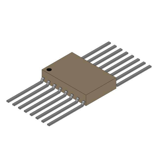
The THS4513 is offered in a 16-pin ceramic flatpack
package (W), and is characterized for operation over
the full military temperature range from –55°C to
125°C.
THS4513 + ADS5424 Circuit
From
50 W
Source
V IN
348 W
100 W
5V
69.8 W
225 W
0.22 mF
THS4513
100 W
49 .9 W
0.22 mF
225 W
2 .7 pF
CM
69.8 W
0.22 mF
348 W
14 Bit,
105 MSPS
A IN+
ADS 5424
A IN– VBG
49.9 W
0.1 mF
0.1 mF
1
Please be aware that an important notice concerning availability, standard warranty, and use in critical applications of
Texas Instruments semiconductor products and disclaimers thereto appears at the end of this data sheet.
PRODUCTION DATA information is current as of publication date.
Products conform to specifications per the terms of the Texas
Instruments standard warranty. Production processing does not
necessarily include testing of all parameters.
Copyright © 2007, Texas Instruments Incorporated
�THS4513-SP
www.ti.com
SLOS539A – SEPTEMBER 2007 – REVISED OCTOBER 2007
This integrated circuit can be damaged by ESD. Texas Instruments recommends that all integrated circuits be handled with
appropriate precautions. Failure to observe proper handling and installation procedures can cause damage.
ESD damage can range from subtle performance degradation to complete device failure. Precision integrated circuits may be more
susceptible to damage because very small parametric changes could cause the device not to meet its published specifications.
PACKAGING/ORDERING INFORMATION (1)
PACKAGED DEVICES
(1)
(2)
TEMPERATURE
CERAMIC FLATPACK
W (16) (2)
SYMBOL
–55°C to 125°C
5962-0722301VFA
5962-0722301VFA
For the most current package and ordering information, see the Package Option Addendum at the end
of this document, or see the TI website at www.ti.com.
Package drawings, thermal data, and symbolization are available at www.ti.com/packaging.
ABSOLUTE MAXIMUM RATINGS (1)
over operating free-air temperature range (unless otherwise noted)
UNIT
VS– to VS+
Supply voltage
6V
VI
Input voltage
±VS
VID
Differential input voltage
IO
Output current
4V
200 mA
Continuous power dissipation
See Dissipation Rating Table
TJ
Maximum junction temperature
TA
Operating free-air temperature range
–55°C to 125°C
Tstg
Storage temperature range
–65°C to 150°C
ESD ratings
(1)
150°C
HBM
2000
CDM
1500
MM
100
The absolute maximum ratings under any condition are limited by the constraints of the silicon process. Stresses above these ratings
may cause permanent damage. Exposure to absolute maximum conditions for extended periods may degrade device reliability. These
are stress ratings only, and functional operation of the device at these or any other conditions beyond those specified is not implied.
DISSIPATION RATING TABLE
2
PACKAGE
θJC
θJA
W (16)
14.7°C/W
189°C/W
Submit Documentation Feedback
POWER RATING
TA ≤ 25°C
TA = 125°C
661 mW
132 mW
Copyright © 2007, Texas Instruments Incorporated
Product Folder Link(s): THS4513-SP
�THS4513-SP
www.ti.com
SLOS539A – SEPTEMBER 2007 – REVISED OCTOBER 2007
SPECIFICATIONS; VS+ – VS– = 5 V (Unchanged after 150 kRad):
Test conditions unless otherwise noted: VS+ = 2.5 V, VS– = –2.5 V, G = 14 dB, CM = open, VO = 2 Vpp, RF = 348 Ω,
RL = 200 Ω Differential, TA = 25°C Single-Ended Input, Differential Output, Input and Output Referenced to Mid-Supply
PARAMETER
TEST CONDITIONS
MIN
TYP
MAX
UNIT
AC PERFORMANCE
Small-Signal Bandwidth
Gain-Bandwidth Product
Bandwidth for 0.1 dB Flatness
Large-Signal Bandwidth
G = 6 dB, VO = 100 mVpp
1.1
GHz
G = 10 dB, VO = 100 mVpp
1.0
GHz
G = 14 dB, VO = 100 mVpp
720
MHz
G = 10 dB
3.0
GHz
G = 10 dB, VO = 2 Vpp
65
G = 14 dB, VO = 2 Vpp
115
G = 6 dB, VO = 2 Vpp
Slew Rate (Differential)
Rise Time Fall Time
3rd Order Harmonic Distortion
2nd Order Intermodulation Distortion
3rd Order Intermodulation Distortion
2 V Step, G = 6 dB
GHz
V/μs
0.5
ns
5.5
f = 10 MHz, RL = 100 Ω
–106
f = 50 MHz, RL = 100 Ω
–90
f = 100 MHz, RL = 100 Ω
–87
f = 10 MHz, RL = 100 Ω
–108
f = 50 MHz, RL = 100 Ω
–106
f = 100 MHz, RL = 100 Ω
–83
VO = 2 Vpp envelope,
200 kHz Tone Spacing,
RL = 100 Ω
2nd Order Output Intercept Point
3rd Order Output Intercept Point
1.1
5100
0.5
Settling Time to 1%
2nd Order Harmonic Distortion
MHz
200 kHz Tone Spacing
RL = 100 Ω
fC = 50 MHz
–83
fC = 100 MHz
–75
fC = 50 MHz
–83
fC = 100 MHz
–74
fC = 50 MHz
84
fC = 100 MHz
77
fC = 50 MHz
42
fC = 100 MHz
Noise Figure
50 Ω System, 10 MHz, G = 6 dB
Input Voltage Noise
Input Current Noise
dBc
dBc
dBc
dBm
38
19.8
dB
f > 10 MHz
2.2
nV/√Hz
f > 10 MHz
1.7
pA/√Hz
DC PERFORMANCE
Open-Loop Voltage Gain (AOL)
Input Offset Voltage
Average Offset Voltage Drift
Input Bias Current
Average Bias Current Drift
Input Offset Current
Average Offset Current Drift
63
TA = 25°C
1
TA = –55°C to 125°C
TA = –55°C to 125°C
TA = 25°C
5.5
8
15.5
20
TA = –55°C to 125°C
20
TA = 25°C
1.6
TA = –55°C to 125°C
Product Folder Link(s): THS4513-SP
mV
μA
nA/°C
3.6
7
4
Submit Documentation Feedback
Copyright © 2007, Texas Instruments Incorporated
mV
μV/°C
2.6
TA = –55°C to 125°C
TA = –55°C to 125°C
dB
4
μA
nA/°C
3
�THS4513-SP
www.ti.com
SLOS539A – SEPTEMBER 2007 – REVISED OCTOBER 2007
SPECIFICATIONS; VS+ – VS– = 5 V (Unchanged after 150 kRad): (continued)
Test conditions unless otherwise noted: VS+ = 2.5 V, VS– = –2.5 V, G = 14 dB, CM = open, VO = 2 Vpp, RF = 348 Ω,
RL = 200 Ω Differential, TA = 25°C Single-Ended Input, Differential Output, Input and Output Referenced to Mid-Supply
PARAMETER
TEST CONDITIONS
MIN
TYP
MAX
UNIT
INPUT
Common-Mode Input Range High
1.75
Common-Mode Input Range Low
–1.75
Common-Mode Rejection Ratio
V
80
Differential Input Impedance
dB
1.67 || 0.5
Common-Mode Input Impedance
MΩ || pF
1.2 || 1.5
OUTPUT
Maximum Output Voltage High
Each output with 100Ω to
mid-supply
Minimum Output Voltage Low
Differential Output Voltage Swing
TA = 25°C
1.2
TA = –55°C to 125°C
1.0
TA = 25°C
1.4
–1.4
TA = –55°C to 125°C
V
–1.2
–1.0
TA = 25°C
4.8
TA = –55°C to 125°C
4.0
5.6
V
V
Differential Output Current Drive
RL = 10 Ω
96
mA
Output Balance Error
VO = 100 mV, f = 1 MHz
–52
dB
Closed-Loop Output Impedance
f = 1 MHz
0.3
Ω
Small-Signal Bandwidth
250
MHz
Slew Rate
110
V/μs
1
V/V
5
mV
±40
μA
OUTPUT COMMON-MODE VOLTAGE CONTROL
Gain
Output Common-Mode Offset
from CM input
–1 V < CM < 1 V
CM Input Bias Current
–1 V < CM < 1 V
CM Input Voltage Range
–1.25 to 1.25
CM Input Impedance
V
23 || 2.8
CM Default Voltage
kΩ || pF
0
V
POWER SUPPLY
Specified Operating Voltage
Maximum Quiescent Current
Minimum Quiescent Current
3
TA = 25°C
5
5.5
37.7
40.9
TA = –55°C to 125°C
42.5
TA = 25°C
34.5
TA = –55°C to 125°C
32.5
Power Supply Rejection (±PSRR)
37.7
V
mA
mA
90
dB
V
POWER DOWN
Enable Voltage Threshold
Referenced to Vs– , Assured on above 2.1 V + VS–
>2.1 + VS–
Disable Voltage Threshold
Assured off below 0.7 V + VS–
10 MHz
2.2
nV/√Hz
f > 10 MHz
1.7
pA/√Hz
DC PERFORMANCE
Open-Loop Voltage Gain (AOL)
Input Offset Voltage
Average Offset Voltage Drift
Input Bias Current
Average Bias Current Drift
Input Offset Current
Average Offset Current Drift
TA = 25°C
TA = –55°C to 125°C
68
dB
1
mV
2.6
μV/°C
6
μA
TA = –55°C to 125°C
20
nA/°C
TA = 25°C
1.6
TA = 25°C
TA = –55°C to 125°C
4
μA
nA/°C
INPUT
Common-Mode Input Range High
0.75
Common-Mode Input Range Low
–0.75
Common-Mode Rejection Ratio
V
80
Differential Input Impedance
1.67 || 0.5
Common-Mode Input Impedance
1.2 || 1.5
dB
MΩ || pF
Submit Documentation Feedback
Copyright © 2007, Texas Instruments Incorporated
Product Folder Link(s): THS4513-SP
5
�THS4513-SP
www.ti.com
SLOS539A – SEPTEMBER 2007 – REVISED OCTOBER 2007
SPECIFICATIONS; VS+ – VS– = 3 V (Unchanged after 150 kRad): (continued)
Test conditions unless otherwise noted: VS+ = 1.5 V, VS– = –1.5 V, G = 14 dB, CM = open, VO = 1 Vpp, RF = 348 Ω, RL =
200 Ω Differential, TA = 25°C Single-Ended Input, Differential Output, Input and Output Referenced to Mid-Supply
PARAMETER
TEST CONDITIONS
TYP
UNIT
0.45
V
–0.45
V
OUTPUT
Maximum Output Voltage High
Minimum Output Voltage Low
Each output with 100 Ω to mid-supply
Differential Output Voltage Swing
1.8
V
50
mA
Differential Output Current Drive
RL = 10 Ω
Output Balance Error
VO = 100 mV, f = 1 MHz
–54
dB
Closed-Loop Output Impedance
f = 1 MHz
0.3
Ω
150
MHz
60
V/μs
1
V/V
OUTPUT COMMON-MODE VOLTAGE CONTROL
Small-Signal Bandwidth
Slew Rate
Gain
Output Common-Mode Offset
from CM input
–0.5 V < CM < 0.5 V
4
mV
CM Input Bias Current
–0.5 V < CM < 0.5 V
±40
μA
CM Input Voltage Range
–1.5 to 1.5
CM Input Impedance
20 || 2.8
CM Default Voltage
0
V
kΩ || pF
V
POWER SUPPLY
Quiescent Current
Power Supply Rejection (±PSRR)
34.8
mA
80
dB
V
POWER DOWN
Enable Voltage Threshold
Referenced to Vs– ,Assured on above 2.1 V + VS–
>2.1
Disable Voltage Threshold
Assured off below 0.7 V + VS–