Product
Folder
Sample &
Buy
Technical
Documents
Support &
Community
Tools &
Software
UC1846-SP
SLUS871D – JANUARY 2009 – REVISED DECEMBER 2016
UC1846-SP Class-V, Radiation Hardened PWM Controller
1 Features
3 Description
•
•
The UC1846-SP control devices provide all of the
necessary features to implement fixed frequency,
current mode control schemes while maintaining a
minimum external parts count. The superior
performance of this technique can be measured in
improved line regulation, enhanced load response
characteristics, and a simpler, easier-to-design
control loop. Topological advantages include inherent
pulse-by-pulse current limiting capability, automatic
symmetry correction for push-pull converters, and the
ability to parallel power modules while maintaining
equal current sharing.
1
•
•
•
•
•
•
•
•
•
•
•
•
•
QML-V Qualified, SMD 5962-86806
5962P8680603VxA:
– Radiation Hardness Assurance (RHA) up to
30-krad(Si) Total Ionizing Dose (TID)
– Passes Functional and Specified PostRadiation Parametric Limits at 45 krad at LDR
(10 mrad(Si)/s) per 1.5× Over Test as Defined
in MIL-STD-883 Test Method 1019.9
Paragraph 3.13.3.b
– Exhibits Low-Dose Rate Sensitivity but
Remains Within the Pre-Radiation Electrical
Limits at 30-krad Total Dose Level, as Allowed
by MIL-STD-883, TM1019
Automatic Feed-Forward Compensation
Programmable Pulse-by-Pulse Current Limiting
Automatic Symmetry Correction in Push-Pull
Configuration
Enhanced Load Response Characteristics
Parallel-Operation Capability for Modular Power
Systems
Differential Current-Sense Amplifier With Wide
Common-Mode Range
Double-Pulse Suppression
500-mA (Peak) Totem-Pole Outputs
±1% Bandgap Reference
Undervoltage Lockout (UVLO)
Soft-Start Capability
Shutdown Terminal
500-kHz Operation
2 Applications
•
•
•
•
•
•
Protection circuitry includes built-in UVLO and
programmable current limit in addition to soft-start
capability. A shutdown function is also available
which can initiate either a complete shutdown with
automatic restart or latch the supply off.
Other features include fully latched operation, doublepulse suppression, deadline adjust capability, a ±1%
trimmed bandgap reference, and low outputs in the
OFF state.
Device Information(1)
PART NUMBER
UC1846-SP
UC1846-SP RHA
PACKAGE
BODY SIZE (NOM)
CDIP (16)
6.92 mm × 19.56 mm
CFP (16)
6.73 mm × 10.30 mm
LCCC (20)
8.89 mm × 8.89 mm
KGD(2)
N/A
CDIP (16)
6.92 mm × 19.56 mm
CFP (16)
6.73 mm × 10.30 mm
(1) For all available packages, see the orderable addendum at
the end of the data sheet.
(2) KGD = known good die
Block Diagram
DC-DC Converters
Satellite Buses and Payloads
Space Launch Vehicles
Undersea Cabling
Available in Military Temperature Range (–55°C to
125°C)
Supports Various Topologies:
– Flyback, Forward, Buck, Boost
– Push-Pull, Half-Bridge, Full Bridge With
External Interface Circuit
1
An IMPORTANT NOTICE at the end of this data sheet addresses availability, warranty, changes, use in safety-critical applications,
intellectual property matters and other important disclaimers. PRODUCTION DATA.
�UC1846-SP
SLUS871D – JANUARY 2009 – REVISED DECEMBER 2016
www.ti.com
Table of Contents
1
2
3
4
5
6
7
Features ..................................................................
Applications ...........................................................
Description .............................................................
Revision History.....................................................
Pin Configuration and Functions .........................
Specifications.........................................................
1
1
1
2
3
6
6.1
6.2
6.3
6.4
6.5
6.6
6
6
6
6
7
8
Absolute Maximum Ratings ......................................
ESD Ratings..............................................................
Recommended Operating Conditions.......................
Thermal Information ..................................................
Electrical Characteristics...........................................
Typical Characteristics ..............................................
Detailed Description .............................................. 9
7.1 Overview ................................................................... 9
7.2 Functional Block Diagram ......................................... 9
7.3 Feature Description................................................... 9
7.4 Device Functional Modes ....................................... 13
8
Application and Implementation ........................ 15
8.1 Application Information............................................ 15
8.2 Typical Applications ................................................ 15
9 Power Supply Recommendations...................... 22
10 Layout................................................................... 22
10.1 Layout Guidelines ................................................. 22
10.2 Layout Example .................................................... 22
11 Device and Documentation Support ................. 23
11.1
11.2
11.3
11.4
11.5
Receiving Notification of Documentation Updates
Community Resources..........................................
Trademarks ...........................................................
Electrostatic Discharge Caution ............................
Glossary ................................................................
23
23
23
23
23
12 Mechanical, Packaging, and Orderable
Information ........................................................... 23
4 Revision History
NOTE: Page numbers for previous revisions may differ from page numbers in the current version.
Changes from Revision C (October 2015) to Revision D
Page
•
Changed title of data sheet from UC1846-SP Rad-Tolerant Class-V, Current-Mode PWM Controller : to UC1846-SP
Class-V, Radiation Hardened PWM Controller....................................................................................................................... 1
•
Added new RHA features to Features section ....................................................................................................................... 1
•
Added RHA package options to Device Information table ..................................................................................................... 1
•
Changed shutdown threshold from 1.0 V : to 350 mV throughout document ........................................................................ 1
•
Added Receiving Notification of Documentation Updates to Device and Documentation Support section ......................... 23
Changes from Revision B (October 2011) to Revision C
Page
•
Added ESD Ratings table, Feature Description section, Device Functional Modes, Application and Implementation
section, Power Supply Recommendations section, Layout section, Device and Documentation Support section, and
Mechanical, Packaging, and Orderable Information section ................................................................................................. 1
•
Added KGD package to Device Information........................................................................................................................... 1
2
Submit Documentation Feedback
Copyright © 2009–2016, Texas Instruments Incorporated
Product Folder Links: UC1846-SP
�UC1846-SP
www.ti.com
SLUS871D – JANUARY 2009 – REVISED DECEMBER 2016
5 Pin Configuration and Functions
FK Package
20-Pin LCCC
Top View
VREF
C/L SS
NC
Shsutdown
VIN
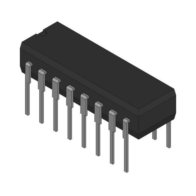
J or W Package
16-Pin CDIP or CFP
Top View
4
3 2
1 20 19
18
17
16
5
6
7
8
15
14
9 10 11 12 13
B Out
VC
NC
Gnd
A Out
1
16
2
15
3
14
4
13
5
12
6
11
7
10
8
9
Shutdown
VIN
B Out
VC
Gnd
A Out
Sync
RT
Comp
CT
NC
RT
Sync
C/S–
C/S+
NC
E/A+
E/A–
C/L SS
VREF
C/S–
C/S+
E/A+
E/A–
Comp
CT
Pin Functions
PIN
NAME
I/O
DESCRIPTION
CDIP or CFP
LCCC
CL SS
1
2
I
Current limit/soft-start.
VREF
2
3
O
5.1-V internally generated reference.
CS-
3
4
I
Inverting input of current sense operational amplifier.
CS+
4
5
I
Non-Inverting input of current sense operational amplifier.
EA+
5
7
I
Non-Inverting input of error amplifier.
EA-
6
8
I
Inverting input of error amplifier.
COMP
7
9
O
Output of error amplifier.
CT
8
10
I
Timing capacitance. Capacitor connected from CT to ground is charged via
current established by RT pin via current mirror. Output pulse dead time is
determined by the size of the capacitor during capacitor discharge time.
RT
9
12
I
Determines oscillator frequency. VREF sources thru RT to create a current
which is mirrored to CT pin.
SYNC
10
13
I/O
Sync pin is an output under normal operation when RT is above 4.1-V sync
output high. Sync pin is an input when RT pin is high and CT pin tied low.
AOUT
11
14
O
Output driver (source/sink).
GND
12
15
—
Ground connection.
VC
13
17
I
Gate drive collector supply voltage. Decouple with capacitor.
BOUT
14
18
O
Output driver (source/sink).
VIN
15
19
I
Input voltage decouple with capacitor.
SHUTDOWN
16
20
I
Shutdown threshold 350 mV. Voltage above threshold latches off oscillator.
NC
—
1, 6, 11
—
No connect.
Submit Documentation Feedback
Copyright © 2009–2016, Texas Instruments Incorporated
Product Folder Links: UC1846-SP
3
�UC1846-SP
SLUS871D – JANUARY 2009 – REVISED DECEMBER 2016
www.ti.com
Bare Die Information
4
DIE THICKNESS
BACKSIDE FINISH
BACKSIDE
POTENTIAL
BOND PAD METALLIZATION
COMPOSITION
BOND PAD
THICKNESS
15 mils
Silicon with backgrind
Floating
AlCu2%
2000 nm
Submit Documentation Feedback
Copyright © 2009–2016, Texas Instruments Incorporated
Product Folder Links: UC1846-SP
�UC1846-SP
www.ti.com
SLUS871D – JANUARY 2009 – REVISED DECEMBER 2016
Bond Pad Coordinates in Microns
DESCRIPTION
PAD NUMBER
X MIN
Y MIN
X MAX
Y MAX
Current limit/soft-start
1
2174.24
1661.16
2280.92
1767.84
VREF
2
2235.2
2026.92
2341.88
2133.6
(–) Current sense
3
1996.44
2219.96
2103.12
2326.64
(+) Current sense
4
1635.76
2219.96
1742.44
2326.64
(+) Error amplifier
5
467.36
2219.96
574.04
2326.64
(–) Error amplifier
6
289.56
2219.96
396.24
2326.64
Compensation
7
142.24
1671.32
248.92
1778
CT
8
157.48
1270
264.16
1376.68
RT
9
157.48
939.8
264.16
1046.48
SYNC
10
157.48
172.72
264.16
279.4
OUTPUT A
11
772.16
213.36
889
350.52
GROUND
12
1346.2
81.28
1463.04
208.28
VC
13
1341.12
472.44
1468.12
645.16
OUTPUT B
14
1920.24
213.36
2037.08
350.52
VIN
15
2255.52
320.04
2362.2
426.72
SHUTDOWN
16
2214.88
1107.44
2321.56
1214.12
Submit Documentation Feedback
Copyright © 2009–2016, Texas Instruments Incorporated
Product Folder Links: UC1846-SP
5
�UC1846-SP
SLUS871D – JANUARY 2009 – REVISED DECEMBER 2016
www.ti.com
6 Specifications
6.1 Absolute Maximum Ratings
over operating free-air temperature range (unless otherwise noted) (1) (2)
MIN
VCC
Supply voltage
Collector supply voltage
VI
Analog input voltage (C/S-, C/S+, E/A+, E/A-, Shutdown)
IO
–0.3
MAX
UNIT
40
V
40
V
VIN
V
Output current, source or sink
500
mA
Reference output current
–30
mA
Sync output current
–5
mA
Error amplifier output current
–5
mA
Soft-start sink current
50
mA
Oscillator charging current
5
mA
TJ(max)
Maximum junction temperature
150
°C
Tlead
Lead temperature (soldering, 10 s)
300
°C
Tstg
Storage temperature
150
°C
(1)
(2)
–65
Stresses beyond those listed under Absolute Maximum Ratings may cause permanent damage to the device. These are stress ratings
only, and functional operation of the device at these or any other conditions beyond those indicated under Recommended Operating
Conditions is not implied. Exposure to absolute-maximum-rated conditions for extended periods may affect device reliability.
All voltages are with respect to ground. Currents are positive into, negative out of the specified terminal.
6.2 ESD Ratings
V(ESD)
(1)
Electrostatic discharge
Human-body model (HBM), per ANSI/ESDA/JEDEC JS-001 (1)
VALUE
UNIT
±2000
V
JEDEC document JEP155 states that 500-V HBM allows safe manufacturing with a standard ESD control process.
6.3 Recommended Operating Conditions
over operating free-air temperature range (unless otherwise noted)
MIN
TJ
Operating junction temperature
NOM
–55
MAX
UNIT
125
°C
6.4 Thermal Information
UC1846-SP
THERMAL METRIC (1)
J (CDIP)
W (CFP)
FK (LCCC)
16 PINS
16 PINS
20 PINS
104.2
105.2
UNIT
RθJA
Junction-to-ambient thermal resistance
N/A
°C/W
RθJC(top)
Junction-to-case (top) thermal resistance
N/A
N/A
N/A
°C/W
RθJB
Junction-to-board thermal resistance
36.6
96.8
N/A
°C/W
ψJT
Junction-to-top characterization parameter
25.0
24.0
N/A
°C/W
ψJB
Junction-to-board characterization parameter
27.9
82.6
N/A
°C/W
RθJC(bot)
Junction-to-case (bottom) thermal resistance
8.2
8.5
9.0
°C/W
(1)
6
For more information about traditional and new thermal metrics, see the Semiconductor and IC Package Thermal Metrics application
report, SPRA953.
Submit Documentation Feedback
Copyright © 2009–2016, Texas Instruments Incorporated
Product Folder Links: UC1846-SP
�UC1846-SP
www.ti.com
SLUS871D – JANUARY 2009 – REVISED DECEMBER 2016
6.5 Electrical Characteristics
VIN = 15 V, RT = 10 kΩ, CT = 4.7 nF, TA = TJ = –55°C to 125°C (unless otherwise noted)
PARAMETER
TEST CONDITIONS
MIN
TYP
MAX
5.04
UNIT
REFERENCE
Output voltage
TJ = 25°C, IO = 1 mA
5.1
5.16
Line regulation
VIN = 8 to 40 V
5
20
mV
Load regulation
IL = 1 to 10 mA
3
15
mV
Temperature stability
Over operating range
Total output variation
Over line, load, and temperature (1)
Output noise voltage
10 Hz ≤ ƒ ≤ 10 kHz, TJ = 25°C (1)
Long-term stability
TJ = 125°C, 1000 hr
Short-circuit output current
VREF = 0 V
–10
Initial accuracy
TJ = 25°C
39
Voltage stability
VIN = 8 to 40 V
Temperature stability
Over operating range
0.4
5
V
mV/°C
5.2
V
100
μV
5
mV
–45
mA
OSCILLATOR
43
47
–1%
2%
–1%
Sync output high level
3.9
Sync output low level
4.35
2.3
Sync input high level
CT = 0 V
Sync input low level
CT = 0 V
Sync input current
Sync = 3.9 V, CT = 0 V
kHz
V
2.5
3.9
V
V
2.5
V
1.3
1.5
mA
0.5
5
mV
250
nA
ERROR AMPLIFIER
Input offset voltage
Input bias current
–1
Input offset current
–0.6
40
0
μA
Common mode range
VIN = 8 to 40 V
Open-loop voltage gain
ΔVO = 1.2 to 3 V, VCM = 2 V
80
Unity-gain bandwidth
TJ = 25°C (1)
0.7
1
CMRR
VCM = 0 to 38 V, VIN = 40 V
75
100
dB
PSRR
VIN = 8 to 40 V
80
105
dB
Output sink current
VID = –15 mV to –5 V, Comp = 1.2 V
Output source current
VID = 15 mV to 5 V, Comp = 2.5 V
High-level output voltage
RL = (Comp) 15 kΩ
Low-level output voltage
RL = (Comp) 15 kΩ
2
VIN – 2
105
4.3
MHZ
6
–0.5
V
dB
mA
–0.4
4.6
mA
V
0.7
1
3.1
V
CURRENT SENSE AMPLIFIER
Amplifier gain
VC/S– = 0 V, C/L SS open (2) (3)
2.5
2.75
Maximum differential input signal
(VC/S+ – VC/S–)
C/L SS open (2), RL (Comp)= 15 kΩ
1.1
1.2
60
83
dB
60
84
dB
–10
–2.5
(2)
Input offset voltage
VC/L SS = 0.5 V, Comp open
CMRR
VCM = 1 to 12 V
PSRR
VIN = 8 to 40 V
Input bias current
VC/L SS = 0.5 V, Comp open (2)
Input offset current
VC/L SS = 0.5 V, Comp open (2)
5
0.08
Input common-mode range
Delay to outputs
(1)
(2)
(3)
TJ = 25°C
(1)
200
V/V
V
25
mV
μA
1
μA
VIN – 3
V
500
ns
Parameters ensured by design and/or characterization, if not production tested.
Parameter measured at trip point of latch with VE/A+ = VREF, VE/A– = 0 V.
Amplifier gain defined as: G = ΔVComp/ΔVC/S+; VC/S+ = 0 to 1 V.
Submit Documentation Feedback
Copyright © 2009–2016, Texas Instruments Incorporated
Product Folder Links: UC1846-SP
7
�UC1846-SP
SLUS871D – JANUARY 2009 – REVISED DECEMBER 2016
www.ti.com
Electrical Characteristics (continued)
VIN = 15 V, RT = 10 kΩ, CT = 4.7 nF, TA = TJ = –55°C to 125°C (unless otherwise noted)
PARAMETER
TEST CONDITIONS
MIN
TYP
MAX
0.55
UNIT
CURRENT LIMIT ADJUST
Current limit offset
VC/S– = 0 V, VC/S+ = 0 V, comp open (2)
0.45
0.5
Input bias current
VE/A+ = VREF, VE/A– = 0 V
–30
–10
250
350
V
μA
SHUTDOWN TERMINAL
Threshold voltage
Input voltage range
0
Minimum latching current (IC/S SS) (4)
3
VIN
1.5
Maximum non-latching current (IC/S SS) (5)
TJ = 25°C (1)
Delay to outputs
400
mV
V
mA
1.5
0.8
mA
300
600
ns
200
μA
0.1
0.4
V
0.4
2.1
V
OUTPUT
Collector-emitter voltage
40
Collector leakage current
V
VC = 40 V
ISINK = 20 mA
Output low-level voltage
ISINK = 100 mA
Output high-level voltage
ISOURCE = 20 mA
13
13.5
ISOURCE = 100 mA
12
13.5
V
V
Rise time
CL = 1 nF, TJ = 25°C (1)
50
300
ns
Fall time
CL = 1 nF, TJ = 25°C (1)
50
300
ns
7.7
8
V
UVLO
Start-up threshold
Threshold hysteresis
0.75
V
TOTAL STANDBY CURRENT
Supply current
(4)
(5)
17
21
mA
Current into C/S SS required to latch circuit in shutdown state.
Current into C/S SS assured not to latch circuit in shutdown state.
110
80
60
40
20
Open-Loop Voltage Gain (dB)
Open-Loop Phase
Open-Loop Voltage Gain (dB)
6.6 Typical Characteristics
o
0
100
1k
10k
100k
1M
0
o
-90
o
-180
100
90
80
70
0
10 20 30
Frequency (Hz)
40 50 60 70
80 90 100
Output Load Resistance RL (k-W)
.
VIN = 20 V
VIN = 20 V
TJ = 25°C
Figure 1. Error Amplifier Gain and Phase vs Frequency
8
TJ = 25°C
Figure 2. Error Amplifier Open-Loop DC Gain vs Load
Resistance
Submit Documentation Feedback
Copyright © 2009–2016, Texas Instruments Incorporated
Product Folder Links: UC1846-SP
�UC1846-SP
www.ti.com
SLUS871D – JANUARY 2009 – REVISED DECEMBER 2016
7 Detailed Description
7.1 Overview
The UC1846-SP control devices provide all of the necessary features to implement fixed frequency, current
mode control schemes while maintaining a minimum external parts count. The superior performance of this
technique can be measured in improved line regulation, enhanced load response characteristics, and a simpler,
easier-to-design control loop. Topological advantages include inherent pulse-by-pulse current limiting capability,
automatic symmetry correction for push-pull converters, and the ability to parallel “power modules" while
maintaining equal current sharing.
7.2 Functional Block Diagram
5.1 V
REFERENCE
REGULATOR
VIN 15
2
VREF
13 VC
SYNC 10
RT
UVLO
LOCKOUT
Q
CT
8
C/S-
3
11 A OUT
T
OSC
Q
Output Stage
COMP
X3
C/S+
F/F
9
S R
Q
4
S
14 B OUT
0.5 V
+
0.5 mA
E/A+
5
E/A–
6
COMP
7
12 GND
E/A
1
C/L SS
16 SHUTDOWN
350 mV
6k
NOTE: Pin numbers shown are for the J package.
7.3 Feature Description
UC1846-SP is a current mode controller, used to support various topologies such as forward, flyback, halfbridge, full bridge, push-pull configurations.
Current mode control is a two-loop system. The switching power supply inductor is hidden within the inner
current control loop. This simplifies the design of the outer voltage control loop and improves power supply
performance in many ways, including better dynamics. The objective of this inner loop is to control the statespace averaged inductor current, but in practice the instantaneous peak inductor current is the basis for control
(switch current, equal to inductor current during the on time, is often sensed). If the inductor ripple current is
small, peak inductor current control is nearly equivalent to average inductor current control.
Submit Documentation Feedback
Copyright © 2009–2016, Texas Instruments Incorporated
Product Folder Links: UC1846-SP
9
�UC1846-SP
SLUS871D – JANUARY 2009 – REVISED DECEMBER 2016
www.ti.com
Feature Description (continued)
The peak method of inductor current control functions by comparing the upslope of inductor current (or switch
current) to a current program level set by the outer loop. The comparator turns the power switch off when the
instantaneous current reaches the desired level. The current ramp is usually quite small compared to the
programming level, especially when VIN is low. As a result, this method is extremely susceptible to noise. A noise
spike is generated each time the switch turns on. A fraction of a volt coupled into the control circuit can cause it
to turn off immediately, resulting in a sub-harmonic operating mode with much greater ripple. Circuit layout and
bypassing are critically important to successful operation.
The peak current mode control method is inherently unstable at duty ratios exceeding 0.5, resulting in subharmonic oscillation. A compensating ramp (with slope equal to the inductor current downslope) is usually
applied to the comparator input to eliminate this instability. A slope compensation must be added to the sensed
current waveform or subtracted from the control voltage to ensure stability above a 50% duty cycle. A
compensating ramp (with slope equal to the inductor current downslope) is usually applied to the comparator
input to eliminate this instability.
The pulse width modulator (PWM) of UC1846-SP is limited to a maximum duty cycle of 50%, thus it can be used
in topologies such as push-pull, half bridge, full bridge, forward, flyback configurations. Limiting PWM to 50%
duty cycle ensures that for isolated or transformer based topologies. The transformer is allowed to reset and
prevent saturation of the transformer core.
Pulse-by-pulse symmetry correction (flux balancing) is inherent to current mode controllers and essential for the
push-pull topology to prevent core saturation.
Current limit control design has numerous advantages:
1. Current mode control provided peak switch current limiting – pulse by pulse current limit.
2. Control loop is simplified as one pole due to output inductor is pushed to higher frequency , thus a two pole
system turns into two real poles. Thus system reduces to a first order system thus simplifies the control.
3. Multiple converter can be paralleled and allows equal current sharing amount the various converters.
4. Inherently provides for input voltage feed-forward as any perturbation in the input voltage will be reflected in
the switch or inductor current. Since switch or inductor current is a direct control input, thus this perturbation
is very rapidly corrected.
5. The error amplifier output (outer control loop) defines the level at which the primary current (inner loop) will
regulate the pulse width, and output voltage.
Ip
V
SENSE
D2
Q1
L1
+
Np
NS
Current
Mode
Control
PWM
+
VIN
–
Np
Q2
IS
C1 VO
–
NS
D1
8
I
SENSE
RS
Figure 3. Push-Pull Converter Using Current Mode Control
7.3.1 Reference
As highlighted in the Functional Block Diagram, UC1846-SP incorporates a 5.1-V internal reference regulator
with ±10% set point variation over temperature.
10
Submit Documentation Feedback
Copyright © 2009–2016, Texas Instruments Incorporated
Product Folder Links: UC1846-SP
�UC1846-SP
www.ti.com
SLUS871D – JANUARY 2009 – REVISED DECEMBER 2016
Feature Description (continued)
7.3.2 Oscillator
Figure 8 highlights the oscillator circuit. Connecting a resistor RT from pin 9 to ground establishes a current,
which is mirrored to pin 8 and charges the capacitor connected from pin 8 to ground. Maximum on time
corresponds to the maximum charging time of the timing capacitor. Oscillator frequency can be determined by
Equation 5.
Off-time corresponds to capacitor discharge time establishes the converter dead time between the pulses
according to Equation 4. Internal 8-mA current sink discharges the CT pin capacitor.
7.3.3 Slope Compensation
For duty cycle above 50% slope compensating can be implemented by using a buffer (that is, 2N2222) and
connecting base to timing capacitor pin 8, collector to VREF (5 V), a resistor in series with emitter connected to
(pin 4) CS+ of differential current sense amplifier. Injecting a downslope proportional to the sawtooth into current
sense amplifier.
As with any bipolar PWM IC, outputs should be protected from negatively biasing the substrate. This is typically
done by using Schottky diodes from ground to each output. Failure to do this could cause spurious interruption
and restart of the oscillator, dropping of output pulses and a significant increase in propagation delays.
7.3.4 Error Amplifier
UC1846-SP incorporates an error amplifier with typical open loop gain of 100 dB and gain bandwidth of 1.5 MHz.
With Source and sink capability of 10 mA and 0.5 mA respectively.
Error amplifier sources up to 0.5 mA.
Figure 4. Error Amplifier Output Configuration
7.3.5 Current Sense Amplifier
UC1846-SP incorporates a differential current sense amplifier which can eliminate ground loop problems and
increase noise immunity. An R-C snubber can also be implemented thus helping in blanking the peak current
spike when the switch is turned on. The input of the current sense amplifier is slew rate limited allowing lower
values of filter capacitors to be used to eliminate leading edge noise.
A small RC filter may be required in some applications to reduce switch transients. Differential input allows remote,
noise-free sensing.
Figure 5. Current-Sense Amplifier Connections
Submit Documentation Feedback
Copyright © 2009–2016, Texas Instruments Incorporated
Product Folder Links: UC1846-SP
11
�UC1846-SP
SLUS871D – JANUARY 2009 – REVISED DECEMBER 2016
www.ti.com
Feature Description (continued)
In some applications, a small RC filter is required to reduce switch transients. Differential input allows remote
noise sensing.
7.3.6 Current Limit
Over current trip point is determined by Equation 1. Differential current sense amplifier has a gain of three, as
shown in Figure 6.
Figure 6. Pulse-By-Pulse Current Limiting
Referring to Figure 6, Equation 1 determines the peak current, Is.
æ R2VREF ö
ç R1 + R2 ÷ - 0.5
ø
Is = è
3RS
(1)
7.3.7 Shutdown
UC1846-SP incorporates a shutdown pin (pin 16). Shutdown threshold voltage is 350 mV. Exceeding the
shutdown threshold voltage causes the device to shutdown.
• If current into ICL_SS VREF/R1 > 3-mA SCR holding current (minimum latch current), then the device latches
off. Power recycle is required to un-latch the device.
• If VREF/R1 < 0.8 mA, that is ICL_SS < 0.8 A, then this ensures that the circuit does not latch in a shutdown
state.
12
Submit Documentation Feedback
Copyright © 2009–2016, Texas Instruments Incorporated
Product Folder Links: UC1846-SP
�UC1846-SP
www.ti.com
SLUS871D – JANUARY 2009 – REVISED DECEMBER 2016
Feature Description (continued)
350 mV
Figure 7. Shutdown Latch
Referring to Figure 11, if
VREF
< 0.8mA
R1
(2)
the shutdown latch commutates when ISS = 0.8 mA and a restart cycle initiates.
Referring to Figure 12, if
VREF
> 3mA
R1
(3)
the device latches off until power is recycled.
7.3.8 Output Section
UC1846-SP incorporates high current dual totem pole output stage capable of sourcing/sinking 1.5-A peak
current for fast switching of power MOSFETs and limited to 0.5-A DC current.
7.3.9 Undervoltage Lockout
Minimum input voltage for converter is 8 V or higher, with typical value being 7.7 V. At input voltages below the
actual UVLO voltage, the devices will not operate.
7.3.10 Soft-Start
Connecting a capacitor from CL/SS pin 1 to ground which is charged by 0.5-mA internal current source will
determine the soft-start time. If over current is also implemented as shown in Figure 6, then SS charge time will
be determined by charging SS capacitor by 0.5-mA current as well as current contributed by R1 resistor in
charging the SS capacitor.
7.4 Device Functional Modes
7.4.1 Operation With VIN < 8 V (Minimum VIN)
The devices operate with input voltages above 8 V. The maximum UVLO voltage is 8 V and will operate at input
voltages above 8 V. The typical UVLO voltage is 7.7 V and the devices may operate at input voltages above that
point. The devices also may operate at lower input voltages, the minimum UVLO voltage is not specified. At input
voltages below the actual UVLO voltage, the devices will not operate.
Submit Documentation Feedback
Copyright © 2009–2016, Texas Instruments Incorporated
Product Folder Links: UC1846-SP
13
�UC1846-SP
SLUS871D – JANUARY 2009 – REVISED DECEMBER 2016
www.ti.com
Device Functional Modes (continued)
7.4.2 Synchronization
The synchronization pin (pin10) can be configured as an output for master/slave application. When the converter
is configured as a master or standalone converter, SYNC (pin 10) is an output. As highlighted in the functional
block diagram, voltage at RT (pin 9) is greater than 4.1-V internal threshold.
When using the part in slave configuration, SYNC pin becomes an input. Typical example of parallel operation
with master/slave configuration is shown in Figure 13. Slave unit CT (pin 8) is grounded and RT pin is connected
to VREF (pin 2).
When using the part in slave configuration, SYNC pin becomes an input. Typical example of parallel operation
with master/slave configuration is shown in Figure 13. Slave unit CT (pin 8) is grounded and RT pin is connected
to VREF (pin 2). Under parallel configuration two or more units can be paralleled, with COMP pins tied together
each will share current equally.
7.4.3 Parallel Operation
Under parallel configuration two or more units can be paralleled, with COMP pins tied together each will share
current equally.
Figure 13 highlights typical parallel operation configuration.
14
Submit Documentation Feedback
Copyright © 2009–2016, Texas Instruments Incorporated
Product Folder Links: UC1846-SP
�UC1846-SP
www.ti.com
SLUS871D – JANUARY 2009 – REVISED DECEMBER 2016
8 Application and Implementation
NOTE
Information in the following applications sections is not part of the TI component
specification, and TI does not warrant its accuracy or completeness. TI’s customers are
responsible for determining suitability of components for their purposes. Customers should
validate and test their design implementation to confirm system functionality.
8.1 Application Information
UC1846-SP can be used as a controller to design various topologies such as push-pull, half-bridge, full bridge,
and flyback.
The following sections highlight the topologies for oscillators, error amplifiers, and parallel configurations
(paralleling two EVMs).
8.2 Typical Applications
8.2.1 Oscillator Circuit Application
VREF
9
Comp
Sawtooth
(Pin 8)
8
RT
7.5 mA
CT
Oscillator
(Pin 10)
10
Output Deadtime (τd)
Sync
A.
Output dead time is determined by the external capacitor, CT, according to the formula:
Wd (µs)
145CT (µF)
ID
3.6
,' ±
RT (k:)
(4)
B.
ID = Oscillator discharge current at 25°C is typically 7.5.
C.
For large values of Wd
D.
Oscillator frequency is approximated by the formula:
¦T N+] |
(µs)
145CT (µF)
2.2
RT (k:) u CT (µF)
(5)
Figure 8. Oscillator Circuit
8.2.1.1 Design Requirements
Table 1. Design Parameters
DESIGN PARAMETER
EXAMPLE VALUE
REFERENCE
Oscillator frequency = 200 kHz
RT = 10 kΩ, CT = 1 nF
Equation 4, Figure 8
Dead time, Td = 75.8 ns
RT = 10 kΩ CT = 1 nF
Equation 5, Figure 8
Submit Documentation Feedback
Copyright © 2009–2016, Texas Instruments Incorporated
Product Folder Links: UC1846-SP
15
�UC1846-SP
SLUS871D – JANUARY 2009 – REVISED DECEMBER 2016
www.ti.com
8.2.1.2 Detailed Design Procedure
8.2.1.2.1 Input Capacitor Selection
Load current, duty cycle, and switching frequency are several factors which determine the magnitude of the input
ripple voltage. Without the input capacitor, the pulsating current of Q1 would need to be completely supplied by
the host source, VIN, which commonly does not have sufficiently low output impedance. Thus there would be
substantial noise on the host DC voltage source and an increase in the conducted EMI on the board. The input
capacitor, CIN, effectively filters the input current so the current from the host DC source is approximately an
average current.
The input ripple voltage amplitude is directly proportional to the output load current. The maximum input ripple
amplitude occurs at maximum output load. Also, the amplitude of the voltage ripple varies with the duty cycle of
the converter.
UC1846-SP requires a high quality ceramic, type X5R or X7R, input decoupling capacitor of at least 47 μF of
effective capacitance on the VIN input voltage pins. In some applications additional bulk capacitance may also be
required for the VIN input. The effective capacitance includes any DC bias effects. The voltage rating of the input
capacitor must be greater than the maximum input voltage. The capacitor must also have a ripple current rating
greater than the maximum input current ripple of the UC1846-SP. The input ripple current can be calculated
using Equation 6.
Icirms = Iout ´
Vout
(Vinmin- Vout)
´
Vinmin
Vinmin
(6)
The value of a ceramic capacitor varies significantly over temperature and the amount of DC bias applied to the
capacitor. The capacitance variations due to temperature can be minimized by selecting a dielectric material that
is stable over temperature. X5R and X7R ceramic dielectrics are usually selected for power regulator capacitors
because they have a high capacitance to volume ratio and are fairly stable over temperature. The output
capacitor must also be selected with the DC bias taken into account. The capacitance value of a capacitor
decreases as the DC bias across a capacitor increases.
The input capacitance value determines the input ripple voltage of the regulator. The input voltage ripple can be
calculated using Equation 7.
Iout max´ 0.25
DVin =
Cin ´ fSW
(7)
8.2.1.2.2 Output Capacitor Selection
The output capacitance of a switching regulator is a vital part of the overall feedback system. The energy storage
inductor and the output capacitor form a second-order low-pass filter.
In switching power supply power stages, the function of output capacitance is to store energy. The energy is
stored in the capacitor’s electric field due to the voltage applied. Thus, qualitatively, the function of a capacitor is
to attempt to maintain a constant voltage.
The value of output capacitance of a buck power stage is generally selected to limit output voltage ripple to the
level required by the specification. Since the ripple current in the output inductor is usually already determined,
the series impedance of the capacitor primarily determines the output voltage ripple. The three elements of the
capacitor that contribute to its impedance (and output voltage ripple) are equivalent series resistance (ESR),
equivalent series inductance (ESL), and capacitance (C). The following gives guidelines for output capacitor
selection.
For continuous inductor current mode operation, to determine the amount of capacitance needed as a function of
inductor current ripple, ΔIL, switching frequency, fS, and desired output voltage ripple, ΔVO, Equation 8 is used
assuming all the output voltage ripple is due to the capacitor’s capacitance.
DIL
C³
8 ´ fS ´ DVO
where ΔIL is the inductor ripple current.
•
16
(8)
Submit Documentation Feedback
Copyright © 2009–2016, Texas Instruments Incorporated
Product Folder Links: UC1846-SP
�UC1846-SP
www.ti.com
SLUS871D – JANUARY 2009 – REVISED DECEMBER 2016
Each capacitor type is characterized by its impedance and the frequency range over which it is most effective.
The frequency at which the impedance reaches its minimum is determined by its ESR and ESL. It is known as
the self resonant frequency of the capacitor. The self resonant frequency is considered to be the maximum
usable frequency for a capacitor. Above this frequency the impedance of the capacitor begins to rise as the ESL
of the capacitor begins to dominate. Note that each capacitor type has a specific frequency band over which it is
most effective. Therefore, a capacitor network of multiple capacitor types is more effective in reducing impedance
than just one type.
The current slew rate of a regulator is limited by its output filter inductor. When the amount of current required by
the load changes, the initial current deficit must be supplied by the output capacitors until the regulator can meet
the load demand.
The desired response to a large change in the load current is the first criteria. The output capacitor needs to
supply the load with current when the regulator control loop can not supply the current. This happens when Load
(ie: memory, processor) has a large and fast increase in current, such as a transition from no load to full load.
The regulator typically needs two or more clock cycles for the control loop to see the change in load current,
output voltage and adjust the duty cycle to react to the change. The output capacitor must be properly sized to
supply the extra current to the Load until the control loop responds to the Load change. The output capacitance
must be large enough to supply the difference in current for 2 clock cycles while only allowing a tolerable amount
of droop in the output voltage. Equation 9 shows the minimum output capacitance necessary to accomplish this.
2 ´ DIout
CO >
fSW ´ DVout
(9)
Where ΔIout is the change in output current, fSW is the regulators switching frequency and ΔVout is the allowable
change in the output voltage. For this example, the transient load response is specified as a 5% change in Vout
for a load step of 1 A. For this example, ΔIout = 1 A and ΔVout = 0.05 × 3.3 = 0.165 V. Using these numbers
gives a minimum capacitance of 25 μF. This value does not take the ESR of the output capacitor into account in
the output voltage change. For ceramic capacitors, the ESR is usually small enough to ignore in this calculation.
8.2.1.2.3 Output Inductor Selection
To calculate the value of the output inductor, use Equation 10. Kind is a coefficient that represents the amount of
inductor ripple current relative to the maximum output current. The inductor ripple current is filtered by the output
capacitor. Therefore, choosing high inductor ripple currents impact the selection of the output capacitor since the
output capacitor must have a ripple current rating equal to or greater than the inductor ripple current. In general,
the inductor ripple value is at the discretion of the designer; however, Kind is normally from 0.1 to 0.3 for the
majority of applications. VinLC refers to the voltage at the input of output LC filter.
VinLC - Vout
Vout
´
L1 =
IO ´ Kind
VinLC ´ fSW
(10)
The current flowing through the inductor is the inductor ripple current plus the output current. During power up,
faults or transient load conditions, the inductor current can increase above the calculated peak inductor current
level calculated above. In transient conditions, the inductor current can increase up to the switch current limit of
the device. For this reason, the most conservative approach is to specify an inductor with a saturation current
rating equal to or greater than the switch current limit rather than the peak inductor current.
8.2.1.2.4 Switching Frequency
Initial accuracy of UC1846-SP oscillator frequency is 200 kHz ±15% over the temperature range. Switching
frequency selection is a trade-off between the overall design size and efficiency. Operating at lower switching
frequency will result in higher efficiency at the expense of larger solution footprint.
Oscillator frequency can be determined as follows:
RT = 10 kΩ
CT = 1 nF
fT =
(11)
(12)
2
RT ´ CT
(13)
(14)
fT = 200 kHz
Submit Documentation Feedback
Copyright © 2009–2016, Texas Instruments Incorporated
Product Folder Links: UC1846-SP
17
�UC1846-SP
SLUS871D – JANUARY 2009 – REVISED DECEMBER 2016
www.ti.com
60
40
20
o
100
VIN = 20 V
18
0
o
-90
o
-180
0
1k
10k
100k
1M
Open-Loop Voltage Gain (dB)
110
80
Open-Loop Phase
Open-Loop Voltage Gain (dB)
8.2.1.3 Application Curves
100
90
80
70
0
Frequency (Hz)
TJ = 25°C
10 20 30
40 50 60 70
80 90 100
Output Load Resistance RL (k-W)
VIN = 20 V
TJ = 25°C
Figure 9. Error Amplifier Gain and Phase vs Frequency
Figure 10. Error Amplifier Open-Loop DC Gain vs Load
Resistance
Figure 11. Shutdown With Auto-Restart
Figure 12. Shutdown Without Auto-Restart (Latched)
Submit Documentation Feedback
Copyright © 2009–2016, Texas Instruments Incorporated
Product Folder Links: UC1846-SP
�UC1846-SP
www.ti.com
SLUS871D – JANUARY 2009 – REVISED DECEMBER 2016
8.2.2 Parallel Operation
Slaving allows parallel operation of two or more units with equal current sharing.
Figure 13. Parallel Operation
8.2.2.1 Design Requirements
Refer to Design Requirements for the oscillator circuit design requirements.
8.2.2.2 Detailed Design Procedure
Refer to Detailed Design Procedure for the oscillator circuit detailed design procedure.
Submit Documentation Feedback
Copyright © 2009–2016, Texas Instruments Incorporated
Product Folder Links: UC1846-SP
19
�UC1846-SP
SLUS871D – JANUARY 2009 – REVISED DECEMBER 2016
www.ti.com
8.2.3 Soft-Start and Shutdown/Restart Functions Application
Current
Limit
Shutdown With Auto-Restart
VREF
< 0.8 mA
R1
A.
If
B.
If
Shutdown With Auto-Restart
(Latched)
VREF
> 3 mA (Latched Off )
R1
VREF
0.8 mA
R1
, the shutdown latch commutates when ISS = 0.8 mA and a restart cycle will be initiated.
VREF
! 3 mA
, the device latches off until power is recycled.
R1
Figure 14. Soft-Start and Shutdown/Restart Functions
20
Submit Documentation Feedback
Copyright © 2009–2016, Texas Instruments Incorporated
Product Folder Links: UC1846-SP
�UC1846-SP
www.ti.com
SLUS871D – JANUARY 2009 – REVISED DECEMBER 2016
8.2.4 Open-Loop Test Circuit Application
Timing Resistor
Frequency Set and
Max Duty Cycle RT
VREF (+5-V Output)
0.1 µF
150 kΩ
10 kΩ
1.8 kΩ
+12
VIN (+12 V)
Sawtooth
0.1 µF
Timing
Capacitor, CT
Sync
+5 V
+5 V
0.1 µF
4.7 nF
1 nF
2 kΩ
2N222
ISENSE
Adjust
(≈1 V PK)
UC1846-SP
IS+
1 kΩ
Shutdown
0.1
1 kΩ
+12
Comp
(+12 V)
1 µF
+5 V
Out A
Inv
–
Duty Cycle
Adjust
150 Ω
Out B
+5 V
Non
150 Ω
1 kΩ
Inv
400 Ω
Current Limit
Adjust
1 kΩ
10 Turn
Gnd
IS+
0.1 µF
IL Adj
A.
Bypass capacitors should be low ESR and ESL type.
B.
Short pins 6 and 7 for unity gain testing.
Ground for
Normal Operation
Figure 15. Open-Loop Test Circuit
Submit Documentation Feedback
Copyright © 2009–2016, Texas Instruments Incorporated
Product Folder Links: UC1846-SP
21
�UC1846-SP
SLUS871D – JANUARY 2009 – REVISED DECEMBER 2016
www.ti.com
9 Power Supply Recommendations
The devices are designed to operate from an input voltage supply range between 8 V and 40 V. This input
supply should be well regulated. If the input supply is located more than a few inches from the UC1846-SP
converter additional bulk capacitance may be required in addition to the ceramic bypass capacitors. A tantalum
capacitor with a value of 47 μF is a typical choice, however this may vary depending upon the output power
being delivered.
10 Layout
10.1 Layout Guidelines
Always try to use a low EMI inductor with a ferrite type closed core. Some examples would be toroid and
encased E core inductors. Open core can be used if they have low EMI characteristics and are located a bit
more away from the low power traces and components. Make the poles perpendicular to the PCB as well if using
an open core. Stick cores usually emit the most unwanted noise.
Each output driver of these devices is capable of 2-A peak currents. Careful layout is essential for correct
operation of the chip. A ground plane must be employed. A unique section of the ground plane must be
designated for high di/dt currents associated with the output stages. Power ground can be separated from the
rest of the ground plane and connected at a single point, although this is not necessary if the high di/dt paths are
well understood and accounted for. VIN should be bypassed directly to power ground with a good high frequency
capacitor. The sources of the power MOSFET should connect to power ground as should the return connection
for input power to the system and the bulk input capacitor. The output should be clamped with a high current
Schottky diode to both VIN and GND. Nothing else should be connected to power ground.
VREF should be bypassed directly to the signal portion of the ground plane with a good high frequency
capacitor. Low ESR/ESL ceramic 1-μF capacitors are recommended for both VIN and VREF. All analog circuitry
should likewise be bypassed to the signal ground plane.
10.2 Layout Example
VIN
VIN
VC
To Analog Circuitry
+
Power
Stage
VIN
+
+
CT
CBULK
AOUT or
BOUT
+
VREF
RTN
GND
Signal Ground
Power Ground
Figure 16. Layout Recommendation
22
Submit Documentation Feedback
Copyright © 2009–2016, Texas Instruments Incorporated
Product Folder Links: UC1846-SP
�UC1846-SP
www.ti.com
SLUS871D – JANUARY 2009 – REVISED DECEMBER 2016
11 Device and Documentation Support
11.1 Receiving Notification of Documentation Updates
To receive notification of documentation updates, navigate to the device product folder on ti.com. In the upper
right corner, click on Alert me to register and receive a weekly digest of any product information that has
changed. For change details, review the revision history included in any revised document.
11.2 Community Resources
The following links connect to TI community resources. Linked contents are provided "AS IS" by the respective
contributors. They do not constitute TI specifications and do not necessarily reflect TI's views; see TI's Terms of
Use.
TI E2E™ Online Community TI's Engineer-to-Engineer (E2E) Community. Created to foster collaboration
among engineers. At e2e.ti.com, you can ask questions, share knowledge, explore ideas and help
solve problems with fellow engineers.
Design Support TI's Design Support Quickly find helpful E2E forums along with design support tools and
contact information for technical support.
11.3 Trademarks
E2E is a trademark of Texas Instruments.
All other trademarks are the property of their respective owners.
11.4 Electrostatic Discharge Caution
These devices have limited built-in ESD protection. The leads should be shorted together or the device placed in conductive foam
during storage or handling to prevent electrostatic damage to the MOS gates.
11.5 Glossary
SLYZ022 — TI Glossary.
This glossary lists and explains terms, acronyms, and definitions.
12 Mechanical, Packaging, and Orderable Information
The following pages include mechanical, packaging, and orderable information. This information is the most
current data available for the designated devices. This data is subject to change without notice and revision of
this document. For browser-based versions of this data sheet, refer to the left-hand navigation.
Submit Documentation Feedback
Copyright © 2009–2016, Texas Instruments Incorporated
Product Folder Links: UC1846-SP
23
�PACKAGE OPTION ADDENDUM
www.ti.com
21-Dec-2016
PACKAGING INFORMATION
Orderable Device
Status
(1)
Package Type Package Pins Package
Drawing
Qty
Eco Plan
Lead/Ball Finish
MSL Peak Temp
(2)
(6)
(3)
Op Temp (°C)
Device Marking
(4/5)
5962-8680601V2A
ACTIVE
LCCC
FK
20
1
TBD
POST-PLATE
N / A for Pkg Type
-55 to 125
59628680601V2A
UC1846L
QMLV
5962-8680601VEA
ACTIVE
CDIP
J
16
1
TBD
A42
N / A for Pkg Type
-55 to 125
5962-8680601VE
A
UC1846JQMLV
5962-8680603V2A
ACTIVE
LCCC
FK
20
1
TBD
POST-PLATE
N / A for Pkg Type
-55 to 125
59628680603V2A
UC1846FK
-SP
5962-8680603V9A
ACTIVE
XCEPT
KGD
0
100
TBD
Call TI
N / A for Pkg Type
-55 to 125
5962-8680603VEA
ACTIVE
CDIP
J
16
1
TBD
A42
N / A for Pkg Type
-55 to 125
5962-8680603VE
A
UC1846J-SP
5962-8680603VFA
ACTIVE
CFP
W
16
1
TBD
A42
N / A for Pkg Type
-55 to 125
5962-8680603VF
A
UC1846W-SP
5962P8680603VEA
ACTIVE
CDIP
J
16
1
TBD
A42
N / A for Pkg Type
-55 to 125
5962P8680603VE
A
UC1846J-SP
5962P8680603VFA
ACTIVE
CFP
W
16
1
TBD
A42
N / A for Pkg Type
-55 to 125
5962P8680603VF
A
UC1846W-SP
(1)
The marketing status values are defined as follows:
ACTIVE: Product device recommended for new designs.
LIFEBUY: TI has announced that the device will be discontinued, and a lifetime-buy period is in effect.
NRND: Not recommended for new designs. Device is in production to support existing customers, but TI does not recommend using this part in a new design.
PREVIEW: Device has been announced but is not in production. Samples may or may not be available.
OBSOLETE: TI has discontinued the production of the device.
(2)
Eco Plan - The planned eco-friendly classification: Pb-Free (RoHS), Pb-Free (RoHS Exempt), or Green (RoHS & no Sb/Br) - please check http://www.ti.com/productcontent for the latest availability
information and additional product content details.
TBD: The Pb-Free/Green conversion plan has not been defined.
Addendum-Page 1
Samples
�PACKAGE OPTION ADDENDUM
www.ti.com
21-Dec-2016
Pb-Free (RoHS): TI's terms "Lead-Free" or "Pb-Free" mean semiconductor products that are compatible with the current RoHS requirements for all 6 substances, including the requirement that
lead not exceed 0.1% by weight in homogeneous materials. Where designed to be soldered at high temperatures, TI Pb-Free products are suitable for use in specified lead-free processes.
Pb-Free (RoHS Exempt): This component has a RoHS exemption for either 1) lead-based flip-chip solder bumps used between the die and package, or 2) lead-based die adhesive used between
the die and leadframe. The component is otherwise considered Pb-Free (RoHS compatible) as defined above.
Green (RoHS & no Sb/Br): TI defines "Green" to mean Pb-Free (RoHS compatible), and free of Bromine (Br) and Antimony (Sb) based flame retardants (Br or Sb do not exceed 0.1% by weight
in homogeneous material)
(3)
MSL, Peak Temp. - The Moisture Sensitivity Level rating according to the JEDEC industry standard classifications, and peak solder temperature.
(4)
There may be additional marking, which relates to the logo, the lot trace code information, or the environmental category on the device.
(5)
Multiple Device Markings will be inside parentheses. Only one Device Marking contained in parentheses and separated by a "~" will appear on a device. If a line is indented then it is a continuation
of the previous line and the two combined represent the entire Device Marking for that device.
(6)
Lead/Ball Finish - Orderable Devices may have multiple material finish options. Finish options are separated by a vertical ruled line. Lead/Ball Finish values may wrap to two lines if the finish
value exceeds the maximum column width.
Important Information and Disclaimer:The information provided on this page represents TI's knowledge and belief as of the date that it is provided. TI bases its knowledge and belief on information
provided by third parties, and makes no representation or warranty as to the accuracy of such information. Efforts are underway to better integrate information from third parties. TI has taken and
continues to take reasonable steps to provide representative and accurate information but may not have conducted destructive testing or chemical analysis on incoming materials and chemicals.
TI and TI suppliers consider certain information to be proprietary, and thus CAS numbers and other limited information may not be available for release.
In no event shall TI's liability arising out of such information exceed the total purchase price of the TI part(s) at issue in this document sold by TI to Customer on an annual basis.
OTHER QUALIFIED VERSIONS OF UC1846-SP :
• Catalog: UC1846
• Enhanced Product: UC1846-EP
NOTE: Qualified Version Definitions:
• Catalog - TI's standard catalog product
• Enhanced Product - Supports Defense, Aerospace and Medical Applications
Addendum-Page 2
����IMPORTANT NOTICE
Texas Instruments Incorporated and its subsidiaries (TI) reserve the right to make corrections, enhancements, improvements and other
changes to its semiconductor products and services per JESD46, latest issue, and to discontinue any product or service per JESD48, latest
issue. Buyers should obtain the latest relevant information before placing orders and should verify that such information is current and
complete. All semiconductor products (also referred to herein as “components”) are sold subject to TI’s terms and conditions of sale
supplied at the time of order acknowledgment.
TI warrants performance of its components to the specifications applicable at the time of sale, in accordance with the warranty in TI’s terms
and conditions of sale of semiconductor products. Testing and other quality control techniques are used to the extent TI deems necessary
to support this warranty. Except where mandated by applicable law, testing of all parameters of each component is not necessarily
performed.
TI assumes no liability for applications assistance or the design of Buyers’ products. Buyers are responsible for their products and
applications using TI components. To minimize the risks associated with Buyers’ products and applications, Buyers should provide
adequate design and operating safeguards.
TI does not warrant or represent that any license, either express or implied, is granted under any patent right, copyright, mask work right, or
other intellectual property right relating to any combination, machine, or process in which TI components or services are used. Information
published by TI regarding third-party products or services does not constitute a license to use such products or services or a warranty or
endorsement thereof. Use of such information may require a license from a third party under the patents or other intellectual property of the
third party, or a license from TI under the patents or other intellectual property of TI.
Reproduction of significant portions of TI information in TI data books or data sheets is permissible only if reproduction is without alteration
and is accompanied by all associated warranties, conditions, limitations, and notices. TI is not responsible or liable for such altered
documentation. Information of third parties may be subject to additional restrictions.
Resale of TI components or services with statements different from or beyond the parameters stated by TI for that component or service
voids all express and any implied warranties for the associated TI component or service and is an unfair and deceptive business practice.
TI is not responsible or liable for any such statements.
Buyer acknowledges and agrees that it is solely responsible for compliance with all legal, regulatory and safety-related requirements
concerning its products, and any use of TI components in its applications, notwithstanding any applications-related information or support
that may be provided by TI. Buyer represents and agrees that it has all the necessary expertise to create and implement safeguards which
anticipate dangerous consequences of failures, monitor failures and their consequences, lessen the likelihood of failures that might cause
harm and take appropriate remedial actions. Buyer will fully indemnify TI and its representatives against any damages arising out of the use
of any TI components in safety-critical applications.
In some cases, TI components may be promoted specifically to facilitate safety-related applications. With such components, TI’s goal is to
help enable customers to design and create their own end-product solutions that meet applicable functional safety standards and
requirements. Nonetheless, such components are subject to these terms.
No TI components are authorized for use in FDA Class III (or similar life-critical medical equipment) unless authorized officers of the parties
have executed a special agreement specifically governing such use.
Only those TI components which TI has specifically designated as military grade or “enhanced plastic” are designed and intended for use in
military/aerospace applications or environments. Buyer acknowledges and agrees that any military or aerospace use of TI components
which have not been so designated is solely at the Buyer's risk, and that Buyer is solely responsible for compliance with all legal and
regulatory requirements in connection with such use.
TI has specifically designated certain components as meeting ISO/TS16949 requirements, mainly for automotive use. In any case of use of
non-designated products, TI will not be responsible for any failure to meet ISO/TS16949.
Products
Applications
Audio
www.ti.com/audio
Automotive and Transportation
www.ti.com/automotive
Amplifiers
amplifier.ti.com
Communications and Telecom
www.ti.com/communications
Data Converters
dataconverter.ti.com
Computers and Peripherals
www.ti.com/computers
DLP® Products
www.dlp.com
Consumer Electronics
www.ti.com/consumer-apps
DSP
dsp.ti.com
Energy and Lighting
www.ti.com/energy
Clocks and Timers
www.ti.com/clocks
Industrial
www.ti.com/industrial
Interface
interface.ti.com
Medical
www.ti.com/medical
Logic
logic.ti.com
Security
www.ti.com/security
Power Mgmt
power.ti.com
Space, Avionics and Defense
www.ti.com/space-avionics-defense
Microcontrollers
microcontroller.ti.com
Video and Imaging
www.ti.com/video
RFID
www.ti-rfid.com
OMAP Applications Processors
www.ti.com/omap
TI E2E Community
e2e.ti.com
Wireless Connectivity
www.ti.com/wirelessconnectivity
Mailing Address: Texas Instruments, Post Office Box 655303, Dallas, Texas 75265
Copyright © 2016, Texas Instruments Incorporated
�