[ /Title
(CD74
HC273
,
CD74
HCT27
3)
/Subject
(High
Speed
CMOS
Logic
Octal
DType
Flip-
CD54HC273, CD74HC273,
CD54HCT273, CD74HCT273
Data sheet acquired from Harris Semiconductor
SCHS174B
High-Speed CMOS Logic
Octal D-Type Flip-Flop with Reset
February 1998 - Revised May 2003
Features
Description
• Common Clock and Asynchronous Master Reset
The ’HC273 and ’HCT273 high speed octal D-Type flip-flops
with a direct clear input are manufactured with silicon-gate
CMOS technology. They possess the low power consumption
of standard CMOS integrated circuits.
• Positive Edge Triggering
• Buffered Inputs
Information at the D inputis transferred to the Q outputs on
the positive-going edge of the clock pulse. All eight flip-flops
are controlled by a common clock (CP) and a common reset
(MR). Resetting is accomplished by a low voltage level
independent of the clock. All eight Q outputs are reset to a
logic 0.
• Fanout (Over Temperature Range)
- Standard Outputs . . . . . . . . . . . . . . . 10 LSTTL Loads
- Bus Driver Outputs . . . . . . . . . . . . . 15 LSTTL Loads
• Wide Operating Temperature Range . . . -55oC to 125oC
• Balanced Propagation Delay and Transition Times
Ordering Information
• Significant Power Reduction Compared to LSTTL
Logic ICs
PART NUMBER
• HC Types
- 2V to 6V Operation
- High Noise Immunity: NIL = 30%, NIH = 30% of VCC
at VCC = 5V
• HCT Types
- 4.5V to 5.5V Operation
- Direct LSTTL Input Logic Compatibility,
VIL= 0.8V (Max), VIH = 2V (Min)
- CMOS Input Compatibility, Il ≤ 1µA at VOL, VOH
TEMP. RANGE (oC)
PACKAGE
CD54HC273F3A
-55 to 125
20 Ld CERDIP
CD74HC273E
-55 to 125
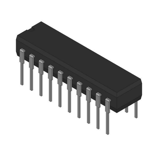
20 Ld PDIP
CD74HC273M
-55 to 125
20 Ld SOIC
CD74HC273M96
-55 to 125
20 Ld SOIC
CD54HCT273F3A
-55 to 125
20 Ld CERDIP
CD74HCT273E
-55 to 125
20 Ld PDIP
CD74HCT273M
-55 to 125
20 Ld SOIC
CD74HCT273M96
-55 to 125
20 Ld SOIC
NOTE: When ordering, use the entire part number. The suffix 96
denotes tape and reel.
Pinout
CD54HC273, CD54HCT273
(CERDIP)
CD74HC273, CD74HCT273
(PDIP, SOIC)
TOP VIEW
MR 1
20 VCC
Q0 2
19 Q7
D0 3
18 D7
D1 4
17 D6
Q1 5
16 Q6
Q2 6
15 Q5
D2 7
14 D5
D3 8
13 D4
Q3 9
12 Q4
GND 10
11 CP
CAUTION: These devices are sensitive to electrostatic discharge. Users should follow proper IC Handling Procedures.
Copyright
© 2003, Texas Instruments Incorporated
1
�CD54/74HC273, CD54/74HCT273
Functional Diagram
CLOCK
CP
DATA
INPUTS
D0
Q0
D1
Q1
D2
Q2
D3
Q3
D4
Q4
D5
Q5
D6
Q6
D7
Q7
DATA
OUTPUTS
RESET MR
TRUTH TABLE
INPUTS
OUTPUT
RESET (MR)
CLOCK CP
DATA Dn
Q
L
X
X
L
H
↑
H
H
H
↑
L
L
H
L
X
Q0
H = High Voltage Level, L = Low Voltage Level, X = Don’t Care, ↑ = Transition from Low to
High Level, Q0 = Level Before the Indicated Steady-State Input Conditions Were Established.
2
�CD54/74HC273, CD54/74HCT273
Absolute Maximum Ratings
Thermal Information
DC Supply Voltage, VCC . . . . . . . . . . . . . . . . . . . . . . . . -0.5V to 7V
DC Input Diode Current, IIK
For VI < -0.5V or VI > VCC + 0.5V . . . . . . . . . . . . . . . . . . . . . .±20mA
DC Output Diode Current, IOK
For VO < -0.5V or VO > VCC + 0.5V . . . . . . . . . . . . . . . . . . . .±20mA
DC Drain Current, per Output, IO
For -0.5V < VO < VCC + 0.5V. . . . . . . . . . . . . . . . . . . . . . . . . .±25mA
DC Output Source or Sink Current per Output Pin, IO
For VO > -0.5V or VO < VCC + 0.5V . . . . . . . . . . . . . . . . . . . .±25mA
DC VCC or Ground Current, ICC . . . . . . . . . . . . . . . . . . . . . . . . .±50mA
Thermal Resistance (Typical, Note 1)
θJC (oC/W)
E (PDIP) Package . . . . . . . . . . . . . . . . . . . . . . . . . . . . . . . . . . 69
M (SOIC) Package. . . . . . . . . . . . . . . . . . . . . . . . . . . . . . . . . . 58
Maximum Junction Temperature . . . . . . . . . . . . . . . . . . . . . . . 150oC
Maximum Storage Temperature Range . . . . . . . . . .-65oC to 150oC
Maximum Lead Temperature (Soldering 10s) . . . . . . . . . . . . . 300oC
(SOIC - Lead Tips Only)
Operating Conditions
Temperature Range, TA . . . . . . . . . . . . . . . . . . . . . . -55oC to 125oC
Supply Voltage Range, VCC
HC Types . . . . . . . . . . . . . . . . . . . . . . . . . . . . . . . . . . . . .2V to 6V
HCT Types . . . . . . . . . . . . . . . . . . . . . . . . . . . . . . . . .4.5V to 5.5V
DC Input or Output Voltage, VI, VO . . . . . . . . . . . . . . . . . 0V to VCC
Input Rise and Fall Time
2V . . . . . . . . . . . . . . . . . . . . . . . . . . . . . . . . . . . . . . 1000ns (Max)
4.5V. . . . . . . . . . . . . . . . . . . . . . . . . . . . . . . . . . . . . . 500ns (Max)
6V . . . . . . . . . . . . . . . . . . . . . . . . . . . . . . . . . . . . . . . 400ns (Max)
CAUTION: Stresses above those listed in “Absolute Maximum Ratings” may cause permanent damage to the device. This is a stress only rating and operation
of the device at these or any other conditions above those indicated in the operational sections of this specification is not implied.
NOTE:
1. The package thermal impedance is calculated in accordance with JESD 51-7.
DC Electrical Specifications
TEST
CONDITIONS
PARAMETER
SYMBOL
VI (V)
VIH
-
25oC
IO (mA) VCC (V)
-40oC TO 85oC
-55oC TO 125oC
MIN
TYP
MAX
MIN
MAX
MIN
MAX
UNITS
2
1.5
-
-
1.5
-
1.5
-
V
4.5
3.15
-
-
3.15
-
3.15
-
V
6
4.2
-
-
4.2
-
4.2
-
V
HC TYPES
High Level Input
Voltage
Low Level Input
Voltage
High Level Output
Voltage
CMOS Loads
VIL
VOH
-
VIH or
VIL
High Level Output
Voltage
TTL Loads
Low Level Output
Voltage
CMOS Loads
VOL
VIH or
VIL
Low Level Output
Voltage
TTL Loads
Input Leakage
Current
Quiescent Device
Current
-
-
2
-
-
0.5
-
0.5
-
0.5
V
4.5
-
-
1.35
-
1.35
-
1.35
V
6
-
-
1.8
-
1.8
-
1.8
V
-0.02
2
1.9
-
-
1.9
-
1.9
-
V
-0.02
4.5
4.4
-
-
4.4
-
4.4
-
V
-0.02
6
5.9
-
-
5.9
-
5.9
-
V
-4
4.5
3.98
-
-
3.84
-
3.7
-
V
-5.2
6
5.48
-
-
5.34
-
5.2
-
V
0.02
2
-
-
0.1
-
0.1
-
0.1
V
0.02
4.5
-
-
0.1
-
0.1
-
0.1
V
0.02
6
-
-
0.1
-
0.1
-
0.1
V
4
4.5
-
-
0.26
-
0.33
-
0.4
V
5.2
6
-
-
0.26
-
0.33
-
0.4
V
II
VCC or
GND
-
6
-
-
±0.1
-
±1
-
±1
µA
ICC
VCC or
GND
0
6
-
-
8
-
80
-
160
µA
3
�CD54/74HC273, CD54/74HCT273
DC Electrical Specifications
(Continued)
TEST
CONDITIONS
SYMBOL
VI (V)
High Level Input
Voltage
VIH
-
-
Low Level Input
Voltage
VIL
-
High Level Output
Voltage
CMOS Loads
VOH
VIH or
VIL
PARAMETER
25oC
IO (mA) VCC (V)
-40oC TO 85oC
-55oC TO 125oC
MIN
TYP
MAX
MIN
MAX
MIN
MAX
UNITS
4.5 to
5.5
2
-
-
2
-
2
-
V
-
4.5 to
5.5
-
-
0.8
-
0.8
-
0.8
V
-0.02
4.5
4.4
-
-
4.4
-
4.4
-
V
-4
4.5
3.98
-
-
3.84
-
3.7
-
V
0.02
4.5
-
-
0.1
-
0.1
-
0.1
V
4
4.5
-
-
0.26
-
0.33
-
0.4
V
HCT TYPES
High Level Output
Voltage
TTL Loads
Low Level Output
Voltage
CMOS Loads
VOL
VIH or
VIL
Low Level Output
Voltage
TTL Loads
II
VCC to
GND
0
5.5
-
-
±0.1
-
±1
-
±1
µA
ICC
VCC or
GND
0
5.5
-
-
8
-
80
-
160
µA
∆ICC
(Note 2)
VCC
-2.1
-
4.5 to
5.5
-
100
360
-
450
-
490
µA
Input Leakage
Current
Quiescent Device
Current
Additional Quiescent
Device Current Per
Input Pin: 1 Unit Load
NOTE:
2. For dual-supply systems theoretical worst case (VI = 2.4V, VCC = 5.5V) specification is 1.8mA.
HCT Input Loading Table
INPUT
UNIT LOADS
MR
1.5
Data
0.4
CP
1.5
NOTE: Unit Load is ∆ICC limit specified in DC Electrical
Specifications table, e.g., 360µA max at 25oC.
Prerequisite For Switching Specifications
PARAMETER
25oC
-40oC TO 85oC -55oC TO 125oC
SYMBOL
TEST
CONDITIONS
VCC
(V)
MIN
TYP
MAX
MIN
MAX
MIN
MAX
UNITS
fMAX
-
2
6
-
-
5
-
4
-
MHz
4.5
30
-
-
25
-
20
-
MHz
6
35
-
-
29
-
23
-
MHz
2
60
-
-
75
-
90
-
ns
HC TYPES
Maximum Clock Frequency
(Figure 1)
MR Pulse Width
(Figure 1)
tW
-
4.5
12
-
-
15
-
18
-
ns
6
10
-
-
13
-
15
-
ns
4
�CD54/74HC273, CD54/74HCT273
Prerequisite For Switching Specifications
PARAMETER
25oC
-40oC TO 85oC -55oC TO 125oC
SYMBOL
TEST
CONDITIONS
VCC
(V)
MIN
TYP
MAX
MIN
MAX
MIN
MAX
UNITS
tW
-
2
80
-
-
100
-
120
-
ns
4.5
16
-
-
20
-
24
-
ns
6
14
-
-
17
-
20
-
ns
2
60
-
-
75
-
70
-
ns
4.5
12
-
-
15
-
18
-
ns
6
10
-
-
13
-
15
-
ns
2
3
-
-
3
-
3
-
ns
4.5
3
-
-
3
-
3
-
ns
6
3
-
-
3
-
3
-
ns
2
50
-
-
65
-
75
-
ns
4.5
10
-
-
13
-
15
-
ns
6
9
-
-
11
-
13
-
ns
Clock Pulse Width (Figure 1)
Set-up Time Data to Clock
(Figure 5)
tSU
Hold Time, Data to Clock
(Figure 5)
-
tH
Removal Time, MR to Clock
(Continued)
-
tREM
-
HCT TYPES
Maximum Clock Frequency
(Figure 2)
fMAX
-
4.5
25
-
-
20
-
16
-
MHz
tw
-
4.5
12
-
-
15
-
18
-
ns
MR Pulse Width
(Figure 2)
Clock Pulse Width (Figure 2)
tw
-
4.5
20
-
-
25
-
30
-
ns
tSU
-
4.5
12
-
-
15
-
18
-
ns
tH
-
4.5
3
-
-
3
-
3
-
ns
tREM
-
4.5
10
-
-
13
-
15
-
ns
Set-up Time Data to Clock
(Figure 6)
Hold Time, Data to Clock
(Figure 6)
Removal Time, MR to Clock
Switching Specifications
PARAMETER
Input tr, tf = 6ns
SYMBOL
TEST
CONDITIONS
tPLH, tPHL
CL = 50pF
25oC
-40oC TO 85oC
-55oC TO
125oC
VCC (V)
TYP
MAX
MAX
MAX
UNITS
2
-
150
190
225
ns
4.5
-
30
38
45
ns
6
-
26
30
38
ns
CL = 15pF
5
12
-
-
-
ns
CL = 50pF
2
-
150
190
225
ns
4.5
-
30
38
45
ns
6
-
26
30
38
ns
2
-
75
95
110
ns
4.5
-
15
19
22
ns
6
-
13
16
19
ns
-
-
10
10
10
pF
5
60
-
-
-
MHz
HC TYPES
Propagation Delay,
Clock to Output
(Figure 3)
Propagation Delay,
MR to Output
(Figure 3)
Output Transition Time
(Figure 3)
Input Capacitance
Maximum Clock Frequency
tPHL
tTLH, tTHL
CI
fMAX
CL = 50pF
CL = 15pF
5
�CD54/74HC273, CD54/74HCT273
Switching Specifications
PARAMETER
Input tr, tf = 6ns (Continued)
25oC
-40oC TO 85oC
-55oC TO
125oC
SYMBOL
TEST
CONDITIONS
VCC (V)
TYP
MAX
MAX
MAX
UNITS
CPD
-
5
25
-
-
-
pF
CL = 50pF
4.5
-
30
38
45
ns
CL = 15pF
5
12
-
-
-
ns
Power Dissipation
Capacitance
(Notes 3, 4)
HCT TYPES
Propagation Delay,
Clock to Output (Figure 4)
tPLH, tPHL
Propagation Delay,
MR to Output (Figure 4)
tPHL
CL = 50pF
4.5
-
32
40
48
ns
Output Transition Time
tTLH, tTHL
CL = 50pF
4.5
-
15
19
22
ns
-
-
10
10
10
pF
5
50
-
-
-
MHz
5
25
-
-
-
pF
Input Capacitance
CIN
Maximum Clock Frequency
fMAX
Power Dissipation
Capacitance
(Notes 3, 4)
CPD
CL = 15pF
-
NOTES:
3. CPD is used to determine the dynamic power consumption, per flip-flop.
4. PD = CPD VCC2 fi + ∑ (CL VCC2 + fO) where fi = Input Frequency, fO = Output Frequency, CL = Output Load Capacitance, VCC = Supply
Voltage.
Test Circuits and Waveforms
tfCL
trCL
CLOCK
tWL + tWH =
90%
10%
I
fCL
CLOCK
50%
50%
1.3V
0.3V
FIGURE 2. HCT CLOCK PULSE RISE AND FALL TIMES AND
PULSE WIDTH
tf = 6ns
tf = 6ns
tr = 6ns
VCC
90%
50%
10%
GND
tTLH
GND
tTHL
90%
50%
10%
INVERTING
OUTPUT
3V
2.7V
1.3V
0.3V
INPUT
tTHL
GND
tWH
NOTE: Outputs should be switching from 10% VCC to 90% VCC in
accordance with device truth table. For fMAX, input duty cycle = 50%.
FIGURE 1. HC CLOCK PULSE RISE AND FALL TIMES AND
PULSE WIDTH
tr = 6ns
1.3V
1.3V
tWL
tWH
NOTE: Outputs should be switching from 10% VCC to 90% VCC in
accordance with device truth table. For fMAX, input duty cycle = 50%.
tPHL
2.7V
0.3V
GND
tWL
INPUT
tfCL = 6ns
I
fCL
3V
VCC
50%
10%
tWL + tWH =
trCL = 6ns
tTLH
90%
1.3V
10%
INVERTING
OUTPUT
tPHL
tPLH
FIGURE 3. HC AND HCU TRANSITION TIMES AND PROPAGATION DELAY TIMES, COMBINATION LOGIC
tPLH
FIGURE 4. HCT TRANSITION TIMES AND PROPAGATION
DELAY TIMES, COMBINATION LOGIC
6
�CD54/74HC273, CD54/74HCT273
Test Circuits and Waveforms
trCL
tfCL
trCL
CLOCK
INPUT
(Continued)
VCC
90%
GND
tH(H)
GND
tH(H)
VCC
DATA
INPUT
50%
tH(L)
3V
1.3V
1.3V
1.3V
GND
tSU(H)
tSU(H)
tSU(L)
tTLH
90%
OUTPUT
tTHL
90%
50%
10%
tTLH
90%
1.3V
OUTPUT
tREM
3V
SET, RESET
OR PRESET
GND
tTHL
1.3V
10%
FIGURE 5. HC SETUP TIMES, HOLD TIMES, REMOVAL TIME,
AND PROPAGATION DELAY TIMES FOR EDGE
TRIGGERED SEQUENTIAL LOGIC CIRCUITS
tPHL
1.3V
GND
IC
CL
50pF
GND
90%
tPLH
50%
IC
tSU(L)
tPHL
tPLH
tREM
VCC
SET, RESET
OR PRESET
1.3V
0.3V
tH(L)
DATA
INPUT
3V
2.7V
CLOCK
INPUT
50%
10%
tfCL
CL
50pF
FIGURE 6. HCT SETUP TIMES, HOLD TIMES, REMOVAL TIME,
AND PROPAGATION DELAY TIMES FOR EDGE
TRIGGERED SEQUENTIAL LOGIC CIRCUITS
7
�PACKAGE OPTION ADDENDUM
www.ti.com
6-Feb-2020
PACKAGING INFORMATION
Orderable Device
Status
(1)
Package Type Package Pins Package
Drawing
Qty
Eco Plan
Lead/Ball Finish
MSL Peak Temp
(2)
(6)
(3)
Op Temp (°C)
Device Marking
(4/5)
5962-8772501RA
ACTIVE
CDIP
J
20
1
TBD
Call TI
N / A for Pkg Type
-55 to 125
5962-8772501RA
CD54HCT273F3A
CD54HC273F
ACTIVE
CDIP
J
20
1
TBD
Call TI
N / A for Pkg Type
-55 to 125
CD54HC273F
CD54HC273F3A
ACTIVE
CDIP
J
20
1
TBD
Call TI
N / A for Pkg Type
-55 to 125
8409901RA
CD54HC273F3A
CD54HCT273F
ACTIVE
CDIP
J
20
1
TBD
Call TI
N / A for Pkg Type
-55 to 125
CD54HCT273F
CD54HCT273F3A
ACTIVE
CDIP
J
20
1
TBD
Call TI
N / A for Pkg Type
-55 to 125
5962-8772501RA
CD54HCT273F3A
CD74HC273E
ACTIVE
PDIP
N
20
20
Pb-Free
(RoHS)
NIPDAU
N / A for Pkg Type
-55 to 125
CD74HC273E
CD74HC273M
ACTIVE
SOIC
DW
20
25
Green (RoHS
& no Sb/Br)
NIPDAU
Level-1-260C-UNLIM
-55 to 125
HC273M
CD74HC273M96
ACTIVE
SOIC
DW
20
2000
Green (RoHS
& no Sb/Br)
NIPDAU
Level-1-260C-UNLIM
-55 to 125
HC273M
CD74HC273M96E4
ACTIVE
SOIC
DW
20
2000
Green (RoHS
& no Sb/Br)
NIPDAU
Level-1-260C-UNLIM
-55 to 125
HC273M
CD74HC273ME4
ACTIVE
SOIC
DW
20
25
Green (RoHS
& no Sb/Br)
NIPDAU
Level-1-260C-UNLIM
-55 to 125
HC273M
CD74HC273MG4
ACTIVE
SOIC
DW
20
25
Green (RoHS
& no Sb/Br)
NIPDAU
Level-1-260C-UNLIM
-55 to 125
HC273M
CD74HCT273E
ACTIVE
PDIP
N
20
20
Pb-Free
(RoHS)
NIPDAU
N / A for Pkg Type
-55 to 125
CD74HCT273E
CD74HCT273EE4
ACTIVE
PDIP
N
20
20
Pb-Free
(RoHS)
NIPDAU
N / A for Pkg Type
-55 to 125
CD74HCT273E
CD74HCT273M
ACTIVE
SOIC
DW
20
25
Green (RoHS
& no Sb/Br)
NIPDAU
Level-1-260C-UNLIM
-55 to 125
HCT273M
CD74HCT273M96
ACTIVE
SOIC
DW
20
2000
Green (RoHS
& no Sb/Br)
NIPDAU
Level-1-260C-UNLIM
-55 to 125
HCT273M
(1)
The marketing status values are defined as follows:
ACTIVE: Product device recommended for new designs.
LIFEBUY: TI has announced that the device will be discontinued, and a lifetime-buy period is in effect.
NRND: Not recommended for new designs. Device is in production to support existing customers, but TI does not recommend using this part in a new design.
PREVIEW: Device has been announced but is not in production. Samples may or may not be available.
Addendum-Page 1
Samples
�PACKAGE OPTION ADDENDUM
www.ti.com
6-Feb-2020
OBSOLETE: TI has discontinued the production of the device.
(2)
RoHS: TI defines "RoHS" to mean semiconductor products that are compliant with the current EU RoHS requirements for all 10 RoHS substances, including the requirement that RoHS substance
do not exceed 0.1% by weight in homogeneous materials. Where designed to be soldered at high temperatures, "RoHS" products are suitable for use in specified lead-free processes. TI may
reference these types of products as "Pb-Free".
RoHS Exempt: TI defines "RoHS Exempt" to mean products that contain lead but are compliant with EU RoHS pursuant to a specific EU RoHS exemption.
Green: TI defines "Green" to mean the content of Chlorine (Cl) and Bromine (Br) based flame retardants meet JS709B low halogen requirements of