SN54ABT7819
512 × 18 × 2
CLOCKED BIDIRECTIONAL FIRST-IN, FIRST-OUT MEMORY
SGBS305D – AUGUST 1994 – REVISED APRIL 1998
D
D
D
D
D
D
D
Member of the Texas Instruments
Widebus Family
Advanced BiCMOS Technology
Free-Running CLKA and CLKB Can Be
Asynchronous or Coincident
Read and Write Operations Synchronized
to Independent System Clocks
Two Separate 512 × 18 Clocked FIFOs
Buffering Data in Opposite Directions
IRA and ORA Synchronized to CLKA
IRB and ORB Synchronized to CLKB
D
D
D
D
D
Microprocessor Interface Control Logic
Programmable Almost-Full/Almost-Empty
Flag
Fast Access Times of 9 ns With a 50-pF
Load and Simultaneous-Switching Data
Outputs
Released as DSCC SMD (Standard
Microcircuit Drawing) 5962-9470401QXA
and 5962-9470401QYA
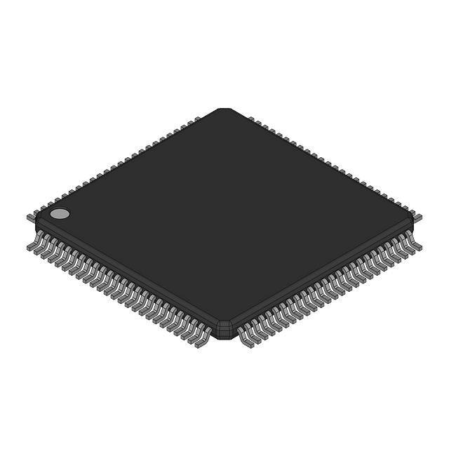
Package Options Include 84-Pin Ceramic
Pin Grid Array (GB) and 84-Pin Ceramic
Quad Flat (HT) Package
W/RB
CSB
RSTB
PENB
PENA
RSTA
CSA
W/RA
GND
WENA
CLKA
RENA
ORA
VCC
NC
VCC
ORB
RENB
CLKB
WENB
GND
HT PACKAGE
(TOP VIEW)
84 83 82 81 80 79 78 77 76 75 74 73 72 71 70 69 68 67 66 65 64
AF/AEA
HFA
IRA
GND
A0
A1
VCC
A2
A3
GND
NC
A4
A5
GND
A6
A7
GND
A8
A9
VCC
A10
1
63
2
62
3
61
4
60
5
59
6
58
7
57
8
56
9
55
10
54
11
53
12
52
13
51
14
50
15
49
16
48
17
47
18
46
19
45
20
44
21
43
AF/AEB
HFB
IRB
GND
B0
B1
VCC
B2
B3
GND
NC
B4
B5
GND
B6
B7
GND
B8
B9
VCC
B10
A14
A15
GND
A16
A17
NC
B17
B16
GND
B15
B14
VCC
B13
B12
GND
B11
A11
GND
A12
A13
VCC
22 23 24 25 26 27 28 29 30 31 32 33 34 35 36 37 38 39 40 41 42
Please be aware that an important notice concerning availability, standard warranty, and use in critical applications of
Texas Instruments semiconductor products and disclaimers thereto appears at the end of this data sheet.
Widebus is a trademark of Texas Instruments Incorporated.
Copyright 1998, Texas Instruments Incorporated
PRODUCTION DATA information is current as of publication date.
Products conform to specifications per the terms of Texas Instruments
standard warranty. Production processing does not necessarily include
testing of all parameters.
On products compliant to MIL-PRF-38535, all parameters are tested
unless otherwise noted. On all other products, production
processing does not necessarily include testing of all parameters.
POST OFFICE BOX 655303
• DALLAS, TEXAS 75265
1
�SN54ABT7819
512 × 18 × 2
CLOCKED BIDIRECTIONAL FIRST-IN, FIRST-OUT MEMORY
SGBS305D – AUGUST 1994 – REVISED APRIL 1998
GB PACKAGE
(TOP VIEW)
1
2
3
4
5
6
7
8
9
10 11
A
B
C
D
E
F
G
H
J
K
L
Terminal Assignments
2
TERMINAL
NAME
TERMINAL
NAME
TERMINAL
NAME
TERMINAL
A1
PENA
B11
IRB
F9
NC
K2
A11
A2
CSA
C1
GND
F10
B6
K3
GND
A3
W/RA
C2
HFA
F11
GND
K4
A4
WENA
C5
CLKA
G1
A5
K5
VCC
GND
A5
ORA
C6
NC
G2
GND
K6
A17
A6
VCC
ORB
C7
A4
K7
GND
C10
VCC
HFB
G3
A7
G9
B4
K8
A8
WENB
C11
GND
G10
GND
K9
VCC
GND
A9
W/RB
D1
A1
G11
B5
K10
B10
A10
CSB
D2
A0
H1
A7
K11
B9
A11
AF/AEB
D10
B0
H2
GND
L1
A10
B1
IRA
D11
B1
H10
GND
L2
A12
B2
AF/AEA
E1
A3
H11
B7
L3
A13
B3
RSTA
E2
A2
J1
A8
L4
A14
B4
GND
E3
J2
A16
RENA
E9
J5
VCC
A15
L5
B5
VCC
VCC
L6
B15
B6
CLKB
E10
B2
J6
NC
L7
B16
B7
RENB
E11
B3
J7
B17
L8
B14
B8
GND
F1
A6
J10
L9
B13
B9
RSTB
F2
GND
J11
VCC
B8
L10
B12
B10
PENB
F3
NC
K1
A9
L11
B11
POST OFFICE BOX 655303
• DALLAS, TEXAS 75265
NAME
�SN54ABT7819
512 × 18 × 2
CLOCKED BIDIRECTIONAL FIRST-IN, FIRST-OUT MEMORY
SGBS305D – AUGUST 1994 – REVISED APRIL 1998
description
A FIFO memory is a storage device that allows data to be read from its array in the same order it is written. The
SN54ABT7819 is a high-speed, low-power BiCMOS bidirectional clocked FIFO memory. Two independent
512 × 18 dual-port SRAM FIFOs on the chip buffer data in opposite directions. Each FIFO has flags to indicate
empty and full conditions, a half-full flag, and a programmable almost-full/almost-empty flag.
The SN54ABT7819 is a clocked FIFO, which means each port employs a synchronous interface. All data
transfers through a port are gated to the low-to-high transition of a continuous (free-running) port clock by enable
signals. The continuous clocks for each port are independent of one another and can be asynchronous or
coincident. The enables for each port are arranged to provide a simple bidirectional interface between
microprocessors and/or buses with synchronous control.
The state of the A0–A17 outputs is controlled by CSA and W/RA. When both CSA and W/RA are low, the outputs
are active. The A0–A17 outputs are in the high-impedance state when either CSA or W/RA is high. Data is
written to FIFOA–B from port A on the low-to-high transition of CLKA when CSA is low, W/RA is high, WENA
is high, and the IRA flag is high. Data is read from FIFOB–A to the A0–A17 outputs on the low-to-high transition
of CLKA when CSA is low, W/RA is low, RENA is high, and the ORA flag is high.
The state of the B0–B17 outputs is controlled by CSB and W/RB. When both CSB and W/RB are low, the outputs
are active. The B0–B17 outputs are in the high-impedance state when either CSB or W/RB is high. Data is
written to FIFOB–A from port B on the low-to-high transition of CLKB when CSB is low, W/RB is high, WENB
is high, and the IRB flag is high. Data is read from FIFOA–B to the B0–B17 outputs on the low-to-high transition
of CLKB when CSB is low, W/RB is low, RENB is high, and the ORB flag is high.
The setup- and hold-time constraints for the chip selects (CSA, CSB) and write/read selects (W/RA, W/RB)
enable and read operations on memory and are not related to the high-impedance control of the data outputs.
If a port read enable (RENA or RENB) and write enable (WENA or WENB) are set low during a clock cycle, the
chip select and write/read select can switch at any time during the cycle to change the state of the data outputs.
The input-ready and output-ready flags of a FIFO are two-stage synchronized to the port clocks for use as
reliable control signals. CLKA synchronizes the status of the input-ready flag of FIFOA–B (IRA) and the
output-ready flag of FIFOB–A (ORA). CLKB synchronizes the status of the input-ready flag of FIFOB–A (IRB)
and the output-ready flag of FIFOA–B (ORB). When the input-ready flag of a port is low, the FIFO receiving input
from the port is full and writes are disabled to its array. When the output-ready flag of a port is low, the FIFO that
outputs data to the port is empty and reads from its memory are disabled. The first word loaded to an empty
memory is sent to the FIFO output register at the same time its output-ready flag is asserted (high). When the
memory is read empty and the output-ready flag is forced low, the last valid data remains on the FIFO outputs
until the output-ready flag is asserted (high) again. In this way, a high on the output-ready flag indicates new
data is present on the FIFO outputs.
The SN54ABT7819 is characterized for operation over the full military temperature range of –55°C to 125°C.
POST OFFICE BOX 655303
• DALLAS, TEXAS 75265
3
�SN54ABT7819
512 × 18 × 2
CLOCKED BIDIRECTIONAL FIRST-IN, FIRST-OUT MEMORY
SGBS305D – AUGUST 1994 – REVISED APRIL 1998
logic symbol†
CLKA
CSA
W/RA
C5
CLOCK A
&
A2
OE1
A3
&
WENA
A4
&
RENA
B5
B3
RSTA
PENA
IRA
ORA
HFA
AF/AEA
A0
A1
A2
A3
A4
A5
A6
A7
A8
A9
A10
A11
A12
A13
A14
A15
A16
A17
A1
B1
A5
C2
B2
D2
Φ
FIFO 512 × 18 × 2
SN54ABT7819
CLOCK B
&
&
READ
ENABLE
FIFOB–A
READ
ENABLE
FIFOA–B
&
INPUT-READY
PORT A
OUTPUT-READY
PORT A
HALF-FULL
FIFOA–B
ALMOST-FULL/EMPTY
FIFOA–B
A8
B7
RESET FIFOB–A
PROGRAM ENABLE
FIFOB–A
INPUT-READY
PORT B
OUTPUT-READY
PORT B
HALF-FULL
FIFOB–A
ALMOST-FULL/EMPTY
FIFOB–A
0
0
D1
B9
B10
B11
A7
C10
A11
D10
D11
E2
E10
E1
E11
G3
G9
G1
G11
F1
F10
H1
H11
J1
1
K1
J11
2
Data
K11
Data
L1
K10
K2
L11
L2
L10
L3
L9
L4
L8
J5
L6
L5
L7
K6
J7
17
17
† This symbol is in accordance with ANSI/IEEE Std 91-1984 and IEC Publication 617-12.
Pin numbers shown are for the GB package.
4
A9
WRITE
ENABLE
FIFOB–A
PROGRAM ENABLE
FIFOA–B
A10
OE2
WRITE
ENABLE
FIFOA–B
RESET FIFOA–B
B6
POST OFFICE BOX 655303
• DALLAS, TEXAS 75265
CLKB
CSB
W/RB
WENB
RENB
RSTB
PENB
IRB
ORB
HFB
AF/AEB
B0
B1
B2
B3
B4
B5
B6
B7
B8
B9
B10
B11
B12
B13
B14
B15
B16
B17
�SN54ABT7819
512 × 18 × 2
CLOCKED BIDIRECTIONAL FIRST-IN, FIRST-OUT MEMORY
SGBS305D – AUGUST 1994 – REVISED APRIL 1998
functional block diagram
PENA
RENA
WENA
CSA
W/RA
CLKA
RSTA
Port-A
Control
Logic
Read
Pointer
18
Register
512 × 18
Dual-Port SRAM
FIFOB–A
Register
18
18
Write
Pointer
Flag
Logic
FIFOB–A
ORA
IRB
AF/AEB
HFB
8
A0–A17
B0–B17
8
IRA
AF/AEA
HFA
Flag
Logic
FIFOA–B
ORB
Write
Pointer
18
Register
512 × 18
Dual-Port SRAM
FIFOA–B
Register
Read
Pointer
Port-B
Control
Logic
RSTB
CLKB
CSB
W/RB
WENB
RENB
PENB
POST OFFICE BOX 655303
• DALLAS, TEXAS 75265
5
�SN54ABT7819
512 × 18 × 2
CLOCKED BIDIRECTIONAL FIRST-IN, FIRST-OUT MEMORY
SGBS305D – AUGUST 1994 – REVISED APRIL 1998
enable logic diagram (positive logic)
CSA
W/RA
WENA
WEN FIFOA–B
Output Enable (A0–A17)
REN FIFOB–A
RENA
CSB
W/RB
WENB
WEN FIFOB–A
Output Enable (B0–B17)
REN FIFOA–B
RENB
Function Tables
A PORT
SELECT INPUTS
CLKA
CSA
W/RA
X
H
↑
L
↑
L
L
A0 A17
A0–A17
OPERATION
WENA
RENA
X
X
X
High Z
None
H
H
X
High Z
Write A0–A17 to FIFOA–B
X
H
Active
Read FIFOB–A to A0–A17
B0 B17
B0–B17
OPERATION
None
B PORT
SELECT INPUTS
6
CLKB
CSB
W/RB
WENB
RENB
X
H
X
X
X
High Z
↑
L
H
H
X
High Z
Write B0–B17 to FIFOB–A
↑
L
L
X
H
Active
Read FIFOA–B to B0–B17
POST OFFICE BOX 655303
• DALLAS, TEXAS 75265
�SN54ABT7819
512 × 18 × 2
CLOCKED BIDIRECTIONAL FIRST-IN, FIRST-OUT MEMORY
SGBS305D – AUGUST 1994 – REVISED APRIL 1998
Terminal Functions
TERMINAL
NAME
I/O
A0–A17
I/O
Port-A data. The 18-bit bidirectional data port for side A.
AF/AEA
O
FIFOA–B almost-full/almost-empty flag. Depth offsets can be programmed for AF/AEA, or the default value of 128 can
be used for both the almost-empty offset (X) and the almost-full offset (Y). AF/AEA is high when X or fewer words or
(512 – Y) or more words are stored in FIFOA–B. AF/AEA is forced high when FIFOA–B is reset.
AF/AEB
O
FIFOB–A almost-full/almost-empty flag. Depth offsets can be programmed for AF/AEB, or the default value of 128 can
be used for both the almost-empty offset (X) and the almost-full offset (Y). AF/AEB is high when X or fewer words or
(512 – Y) or more words are stored in FIFOB–A. AF/AEB is forced high when FIFOB–A is reset.
B0–B17
I/O
Port-B data. The 18-bit bidirectional data port for side B.
DESCRIPTION
CLKA
I
Port-A clock. CLKA is a continuous clock that synchronizes all data transfers through port A to its low-to-high transition
and can be asynchronous or coincident to CLKB.
CLKB
I
Port-B clock. CLKB is a continuous clock that synchronizes all data transfers through port B to its low-to-high transition
and can be asynchronous or coincident to CLKA.
CSA
I
Port-A chip select. CSA must be low to enable a low-to-high transition of CLKA to either write data from A0–A17 to
FIFOA–B or read data from FIFOB–A to A0–A17. The A0–A17 outputs are in the high-impedance state when CSA
is high.
CSB
I
Port-B chip select. CSB must be low to enable a low-to-high transition of CLKB to either write data from B0–B17 to
FIFOB–A or read data from FIFOA–B to B0–B17. The B0–B17 outputs are in the high-impedance state when CSB
is high.
HFA
O
FIFOA–B half-full flag. HFA is high when FIFOA–B contains 256 or more words and is low when FIFOA–B contains
255 or fewer words. HFA is set low after FIFOA–B is reset.
HFB
O
FIFOB–A half-full flag. HFB is high when FIFOB–A contains 256 or more words and is low when FIFOB–A contains
255 or fewer words. HFB is set low after FIFOB–A is reset.
IRA
O
Port-A input-ready flag. IRA is synchronized to the low-to-high transition of CLKA. When IRA is low, FIFOA–B is full
and writes to its array are disabled. IRA is set low during a FIFOA–B reset and is set high on the second low-to-high
transition of CLKA after reset.
IRB
O
Port-B input-ready flag. IRB is synchronized to the low-to-high transition of CLKB. When IRB is low, FIFOB–A is full
and writes to its array are disabled. IRB is set low during a FIFOB–A reset and is set high on the second low-to-high
transition of CLKB after reset.
O
Port-A output-ready flag. ORA is synchronized to the low-to-high transition of CLKA. When ORA is low, FIFOB–A is
empty and reads from its array are disabled. The last valid word remains on the FIFOB–A outputs when ORA is low.
Ready data is present for the A0–A17 outputs when ORA is high. ORA is set low during a FIFOB–A reset and goes
high on the third low-to-high transition of CLKA after the first word is loaded to an empty FIFOB–A.
ORB
O
Port-B output-ready flag. ORB is synchronized to the low-to-high transition of CLKB. When ORB is low, FIFOA–B is
empty and reads from its array are disabled. The last valid word remains on the FIFOA–B outputs when ORB is low.
Ready data is present for the B0–B17 outputs when ORB is high. ORB is set low during a FIFOA–B reset and goes
high on the third low-to-high transition of CLKB after the first word is loaded to an empty FIFOA–B.
PENA
I
AF/AEA program enable. After FIFOA–B is reset and before a word is written to its array, the binary value on A0–A7
is latched as an AF/AEA offset when PENA is low and CLKA is high.
PENB
I
AF/AEB program enable. After FIFOB–A is reset and before a word is written to its array, the binary value on B0–B7
is latched as an AF/AEB offset when PENB is low and CLKB is high.
RENA
I
Port-A read enable. A high level on RENA enables data to be read from FIFOB–A on the low-to-high transition of CLKA
when CSA is low, W/RA is low, and ORA is high.
RENB
I
Port-B read enable. A high level on RENB enables data to be read from FIFOA–B on the low-to-high transition of CLKB
when CSB is low, W/RB is low, and ORB is high.
RSTA
I
FIFOA–B reset. To reset FIFOA–B, four low-to-high transitions of CLKA and four low-to-high transitions of CLKB must
occur while RSTA is low. This sets HFA low, IRA low, ORB low, and AF/AEA high.
RSTB
I
FIFOB–A reset. To reset FIFOB–A, four low-to-high transitions of CLKA and four low-to-high transitions of CLKB must
occur while RSTB is low. This sets HFB low, IRB low, ORA low, and AF/AEB high.
ORA
POST OFFICE BOX 655303
• DALLAS, TEXAS 75265
7
�SN54ABT7819
512 × 18 × 2
CLOCKED BIDIRECTIONAL FIRST-IN, FIRST-OUT MEMORY
SGBS305D – AUGUST 1994 – REVISED APRIL 1998
Terminal Functions (Continued)
TERMINAL
NAME
I/O
DESCRIPTION
WENA
I
Port-A write enable. A high level on WENA enables data on A0–A17 to be written into FIFOA–B on the low-to-high
transition of CLKA when W/RA is high, CSA is low, and IRA is high.
WENB
I
Port-B write enable. A high level on WENB enables data on B0–B17 to be written into FIFOB–A on the low-to-high
transition of CLKB when W/RB is high, CSB is low, and IRB is high.
W/RA
I
Port-A write/read select. A high on W/RA enables A0–A17 data to be written to FIFOA–B on a low-to-high transition
of CLKA when WENA is high, CSA is low, and IRA is high. A low on W/RA enables data to be read from FIFOB–A
on a low-to-high transition of CLKA when RENA is high, CSA is low, and ORA is high. The A0–A17 outputs are in the
high-impedance state when W/RA is high.
I
Port-B write/read select. A high on W/RB enables B0–B17 data to be written to FIFOB–A on a low-to-high transition
of CLKB when WENB is high, CSB is low, and IRB is high. A low on W/RB enables data to be read from FIFOA–B
on a low-to-high transition of CLKB when RENB is high, CSB is low, and ORB is high. The B0–B17 outputs are in the
high-impedance state when W/RB is high.
W/RB
CLKA
1
CLKB
1
2
3
2
4
3
1
4
RSTA
ÎÎÎÎÎÎÎÎÎÎÎÎ
ÎÎÎÎÎÎÎÎÎÎÎÎ
ÎÎÎÎÎÎÎÎÎÎÎÎÎÎÎÎ
ÎÎÎÎÎÎÎÎÎÎÎÎÎÎÎÎ
ÎÎÎÎÎ
ÎÎÎÎÎ
ÏÏÏÏÏ
ÏÏÏÏÏ
IRA
ORB
HFA
AF/AEA
Figure 1. Reset Cycle for FIFOA–B†
† FIFOB–A is reset in the same manner.
8
POST OFFICE BOX 655303
• DALLAS, TEXAS 75265
2
�SN54ABT7819
512 × 18 × 2
CLOCKED BIDIRECTIONAL FIRST-IN, FIRST-OUT MEMORY
SGBS305D – AUGUST 1994 – REVISED APRIL 1998
CLKA
1
IRA
0
CSA
ÌÌÌÌÌÌ
ÌÌÌÌÌÌÌÌ
ÌÌÌ
ÌÌÌÌÌÌ
ÌÌÌÌÌÌÌÌ
ÌÌÌ
ÌÌÌÌÌÌÌÌÌÌÌÌÌÌÌÌÌÌÌÌÌÌÌ
ÌÌÌÌÌÌÌÌÌ
ÌÌÌÌÌÌÌÌÌÌÌÌÌÌÌÌÌÌÌÌÌÌÌ
ÌÌÌÌÌÌÌÌÌ
ÌÌÌÌÌÌÌÌ
ÌÌÌÌÌ
ÌÌÌÌÌÌÌÌÌÌ
ÌÌÌÌÌÌ
ÌÌÌ
ÌÌÌÌÌÌ ÌÌÌ ÌÌÌÌÌÌÌÌ ÌÌÌ ÌÌÌ
ÌÌÌÌÌÌ ÌÌÌ ÌÌÌÌÌÌÌÌ ÌÌÌ ÌÌÌ
W/RA
WENA
A0–A17
Word 1†
Word 2†
Word 3†
Word 4†
† Written to FIFOA–B
Figure 2. Write Timing – Port A
CLKB
1
IRB
0
CSB
ÌÌÌÌÌÌ
ÌÌÌÌÌÌÌÌ
ÌÌÌ
ÌÌÌÌÌÌ
ÌÌÌÌÌÌÌÌ
ÌÌÌ
ÌÌÌÌÌÌÌÌÌÌÌÌÌÌÌÌÌÌÌÌÌÌÌ
ÌÌÌÌÌÌÌÌÌ
ÌÌÌÌÌÌÌÌ
ÌÌÌÌÌ
ÌÌÌÌÌÌÌÌÌÌ
ÌÌÌÌÌÌ
ÌÌÌ
ÌÌÌÌÌÌ ÌÌÌ ÌÌÌÌÌÌÌÌ ÌÌÌ ÌÌÌ
ÌÌÌÌÌÌ ÌÌÌ ÌÌÌÌÌÌÌÌ ÌÌÌ ÌÌÌ
W/RB
WENB
B0–B17
Word 1‡
Word 2‡
Word 3‡
Word 4‡
‡ Written to FIFOB–A
Figure 3. Write Timing – Port B
POST OFFICE BOX 655303
• DALLAS, TEXAS 75265
9
�SN54ABT7819
512 × 18 × 2
CLOCKED BIDIRECTIONAL FIRST-IN, FIRST-OUT MEMORY
SGBS305D – AUGUST 1994 – REVISED APRIL 1998
CLKA
1
CSA
0
1
W/RA
ÏÏÏÏÏÎÎÎÎÎ
ÏÏÏÏÏ
ÎÎÎÎÎ
ÌÌÌÌÌ ÌÌÌÌÌÌÌÌÌÌÌÌÌÌÌÌÌÌÌÌÌÌÌÌ
ÌÌÌÌÌ ÌÌÌÌÌÌÌÌÌÌÌÌÌÌÌÌÌÌÌÌÌÌÌÌ
WENA
tsu
A0–A17
CLKB
W1
1
2
3
ORB
tpd
tpd
CSB
W/RB
ÏÏÏÏÏÏÏÏÏÏÏÏÏÏÏÏÏÏÏÏ
ÎÎÎÎÎÎÎÎÎÎÎ
ÏÏÏÏÏÏÏÏÏÏÏÏÏÏÏÏÏÏÏÏ
ÎÎÎÎÎÎÎÎÎÎÎ
ÌÌÌÌÌÌÌÌÌÌÌÌÌÌÌÌ
ÌÌÌÌÌÌÌÌÌÌÌÌÌÌÌÌ
RENB
tpd
B0–B17
W1 From FIFOA–B
Figure 4. ORB-Flag Timing and First Data-Word Fall-Through When FIFOA–B Is Empty†
† Operation of FIFOB–A is identical to that of FIFOA–B.
10
POST OFFICE BOX 655303
• DALLAS, TEXAS 75265
0
�SN54ABT7819
512 × 18 × 2
CLOCKED BIDIRECTIONAL FIRST-IN, FIRST-OUT MEMORY
SGBS305D – AUGUST 1994 – REVISED APRIL 1998
CLKB
1
CSB
0
1
W/RB
RENB
0
ÏÏÏ ÎÎÎÎ
ÏÏÏ ÎÎÎÎ
From FIFOA–B
B0–B17
CLKA
1
2
IRA
tpd
tpd
1
CSA
0
WENA
ÏÏÏÏÏÏÏÏÏÏÏÏÏÏÏÎÎÎÎÎÎÎÎÎÎÎÎÎÎÎ
ÏÏÏÏÏÏÏÏÏÏÏÏÏÏÏÎÎÎÎÎÎÎÎÎÎÎÎÎÎÎ
1
W/RA
0
A0–A17
ÌÌÌÌÌÌÌÌÌÌÌÌÌÌÌ ÌÌÌÌÌÌÌÌÌÌÌÌÌ
ÌÌÌÌÌÌÌÌÌÌÌÌÌÌÌ ÌÌÌÌÌÌÌÌÌÌÌÌÌ
To FIFOA–B
Figure 5. Write-Cycle and IRA-Flag Timing When FIFOA–B Is Full†
† Operation of FIFOB–A is identical to that of FIFOA–B.
POST OFFICE BOX 655303
• DALLAS, TEXAS 75265
11
�SN54ABT7819
512 × 18 × 2
CLOCKED BIDIRECTIONAL FIRST-IN, FIRST-OUT MEMORY
SGBS305D – AUGUST 1994 – REVISED APRIL 1998
CLKA
1
ORA
0
CSA
ÎÎÎÎ
ÏÏÏÏÏÏÏ
ÎÎÎÎ
ÏÏÏÏÏÏÏ
ÎÎÎÎ
ÏÏÏÏÏÏÏ
ÌÌÌÌÌÌÌÌÌÌÌÌÌÌÌÌÌÌÌÌÌÌÌÌÌÌÌÌÌÌ
ÌÌÌÌÌÌÌÌÌÌÌÌÌÌÌÌÌÌÌÌÌÌÌÌÌÌÌÌÌÌ
W/RA
RENA
ten
tpd
Word 1†
A0–A17
tdis
Word 2†
Word 3†
Word 4†
† Read from FIFOB–A
Figure 6. Read Timing – Port A
CLKB
1
ORB
0
CSB
ÎÎÎÎ
ÏÏÏÏÏÏÏ
ÎÎÎÎ
ÏÏÏÏÏÏÏ
ÌÌÌÌÌÌÌÌÌÌÌÌÌÌÌÌÌÌÌÌÌÌÌÌÌÌÌÌÌÌ
ÌÌÌÌÌÌÌÌÌÌÌÌÌÌÌÌÌÌÌÌÌÌÌÌÌÌÌÌÌÌ
ÌÌÌÌÌÌÌÌÌÌÌÌÌÌÌÌÌÌÌÌÌÌÌÌÌÌÌÌÌÌ
W/RB
RENB
ten
B0–B17
tpd
Word 1‡
tdis
Word 2‡
Word 3‡
‡ Read from FIFOA–B
Figure 7. Read Timing – Port B
12
POST OFFICE BOX 655303
• DALLAS, TEXAS 75265
Word 4‡
�CLKA
WENA
ÌÌÌ
ÌÌÌÌÌÌ
ÌÌÌ
ÌÌÌÌÌÌ
ÌÌÌÌÌÌ
ÌÌÌ
ÌÌÌÌÌÌ
ÌÌÌÌÌÌ
ÌÌÌ
ÌÌÌ
ÌÌÌ
ÌÌÌ
ÌÌÌÌÌÌ
ÌÌÌ
ÌÌÌÌÌÌ
ÌÌÌ
ÌÌÌ
ÌÌÌ
ÌÌÌÌÌÌ
ÌÌÌ
ÌÌÌ
ÌÌÌ
ÌÌÌÌÌÌ
ÌÌÌ
ÌÌÌ
ÌÌÌ
ÌÌÌ
ÌÌÌ
IRA
A0–A17
W1
WX+1
WX+2
W256
W257
W512–Y
W513–Y
W513
RENB
B0–B17
W1
W2
WY+1
WY+2
AF/AEA
HFA
NOTES: A. CSA, CSB = 0, W/RA = 1, W/RB = 0
B. X is the almost-empty offset and Y is the almost-full offset for AF/AEA.
C. HFB and AF/AEB function in the same manner for FIFO B – A.
Figure 8. FIFOA – B (HFA, AF/AEA) Asynchronous Flag Timing
W257
W258
W512–X
W513–X
13
SGBS305D – AUGUST 1994 – REVISED APRIL 1998
ÌÌÌ
ÌÌÌ
ÌÌÌ
ÌÌÌ
• DALLAS, TEXAS 75265
ORB
SN54ABT7819
512 × 18 × 2
CLOCKED BIDIRECTIONAL FIRST-IN, FIRST-OUT MEMORY
POST OFFICE BOX 655303
CLKB
�SN54ABT7819
512 × 18 × 2
CLOCKED BIDIRECTIONAL FIRST-IN, FIRST-OUT MEMORY
SGBS305D – AUGUST 1994 – REVISED APRIL 1998
offset values for AF/AE
The AF/AE flag of each FIFO has two programmable limits: the almost-empty offset value (X) and the almost-full
offset value (Y). They can be programmed from the input of the FIFO after it is reset and before a word is written
to its memory. An AF/AE flag is high when its FIFO contains X or fewer words or (512 – Y) or more words.
To program the offset values for AF/AEA, PENA can be brought low after FIFOA–B is reset and only when CLKA
is low. On the following low-to-high transition of CLKA, the binary value on A0–A7 is stored as the almost-empty
offset value (X) and the almost-full offset value (Y). Holding PENA low for another low-to-high transition of CLKA
reprograms Y to the binary value on A0–A7 at the time of the second CLKA low-to-high transition.
During the first two CLKA cycles used for offset programming, PENA can be brought high only when CLKA is
low. PENA can be brought high at any time after the second CLKA pulse used for offset programming returns
low. A maximum value of 255 can be programmed for either X or Y (see Figure 9). To use the default values
of X = Y = 128, PENA must be tied high. No data is stored in FIFOA–B while the AF/AEA offsets are programmed.
The AF/AEB flag is programmed in the same manner, with PENB enabling CLKB to program the offset values
taken from B0–B7.Figure 8
RESET
CLKA
3
4
IRA
ÏÏÏÏÏÏÏÏ
ÎÎ
ÏÏÏÏÏÏÏÏÏ
ÏÏÏÏÏÏÏÏ
ÎÎ
ÏÏÏÏÏÏÏÏÏ
ÏÏÏÏÏÏÏÏÏÏÏÏÏÏÏÏÏÏÏÏÏÏÏÏ
ÏÏÏÏÏÏÏÏÏÏÏÏÏÏÏÏÏÏÏÏÏÏÏÏ
ÏÏÏÏÏÏÏÏÏÏÏÏÏÏÏÏÏÏÏÏÏÏÏÏ
ÏÏÏÏÏÏÏÏÏÏÏÏÏ
ÏÏÏÏÏÏÏÏÏÏÏÏÏ
ÏÏÏÏÏÏÏÏÏÏÏÏÏ
ÎÎÎÎÎÎÎÎÎÎÎÎÎÎÎÎÎÎÎÎÎÎÎÎ
ÎÎÎÎÎÎÎÎÎÎÎÎÎÎÎÎÎÎÎÎÎÎÎÎ
ÌÌÌÌÌÌÌÌÌÌÌÌÌÌÌ
ÌÌÌÌÌÌÌÌ
ÌÌÌÌÌÌÌÌÌÌÌÌÌÌÌ
ÌÌÌÌÌÌÌÌ
PENA
CSA
W/RA
WENA
A0–A7
X and Y
Y
Figure 9. Programming X and Y Separately for AF/AEA
14
POST OFFICE BOX 655303
• DALLAS, TEXAS 75265
�SN54ABT7819
512 × 18 × 2
CLOCKED BIDIRECTIONAL FIRST-IN, FIRST-OUT MEMORY
SGBS305D – AUGUST 1994 – REVISED APRIL 1998
absolute maximum ratings over operating free-air temperature range (unless otherwise noted)†
Supply voltage range, VCC . . . . . . . . . . . . . . . . . . . . . . . . . . . . . . . . . . . . . . . . . . . . . . . . . . . . . . . . . . –0.5 V to 7 V
Input voltage range, VI (see Note 1) . . . . . . . . . . . . . . . . . . . . . . . . . . . . . . . . . . . . . . . . . . . –0.5 V to VCC + 0.5 V
Voltage range applied to any output in the high state or power-off state, VO . . . . . . . . . . . . . . –0.5 V to 5.5 V
Current into any output in the low state, IO . . . . . . . . . . . . . . . . . . . . . . . . . . . . . . . . . . . . . . . . . . . . . . . . . . 48 mA
Input clamp current, IIK (VI < 0) . . . . . . . . . . . . . . . . . . . . . . . . . . . . . . . . . . . . . . . . . . . . . . . . . . . . . . . . . . . –18 mA
Output clamp current, IOK (VO < 0) . . . . . . . . . . . . . . . . . . . . . . . . . . . . . . . . . . . . . . . . . . . . . . . . . . . . . . . . –50 mA
Storage temperature range, Tstg . . . . . . . . . . . . . . . . . . . . . . . . . . . . . . . . . . . . . . . . . . . . . . . . . . . –65°C to 150°C
† Stresses beyond those listed under “absolute maximum ratings” may cause permanent damage to the device. These are stress ratings only, and
functional operation of the device at these or any other conditions beyond those indicated under “recommended operating conditions” is not
implied. Exposure to absolute-maximum-rated conditions for extended periods may affect device reliability.
NOTE 1: The input and output negative-voltage ratings may be exceeded if the input and output clamp-current ratings are observed.
recommended operating conditions
VCC
VIH
Supply voltage
VIL
VI
Low-level input voltage
IOH
IOL
∆t/∆v
Input transition rise or fall rate
TA
Operating free-air temperature
High-level input voltage
MIN
NOM
MAX
4.5
5
5.5
2
UNIT
V
V
0.8
V
V
High-level output current
VCC
–12
Low-level output current
24
mA
5
ns/V
Input voltage
0
–55
125
mA
°C
electrical characteristics over recommended operating free-air temperature range (unless
otherwise noted)
PARAMETER
VIK
TEST CONDITIONS
VCC = 4.5 V,
VCC = 4.5 V,
II = –18 mA
IOH = –3 mA
VCC = 5 V,
VCC = 4.5 V,
IOH = –3 mA
IOH = –12 mA
VOL
II
VCC = 4.5 V,
VCC = 5.5 V,
IOL = 24 mA
VI = VCC or GND
IOZH§
IOZL§
VCC = 5.5 V,
VCC = 5.5 V,
VO = 2.7 V
VO = 0.5 V
IO¶
VCC = 5.5 V,
VO = 2.5 V
VOH
ICC
VCC = 5.5 V,
Ci
Control inputs
Co
Flags
Cio
A or B ports
IO = 0,
MIN
TYP‡
MAX
UNIT
–1.2
V
2.5
2
0.5
–40
VI = VCC or GND
–100
0.55
V
±1
µA
50
µA
– 50
µA
–180
mA
Outputs high
15
Outputs low
95
Outputs disabled
15
VI = 2.5 V or 0.5 V
VO = 2.5 V or 0.5 V
VO = 2.5 V or 0.5 V
‡ All typical values are at VCC = 5 V, TA = 25°C.
§ The parameters IOZH and IOZL include the input leakage current.
¶ Not more than one output should be tested at a time, and the duration of the test should not exceed one second.
POST OFFICE BOX 655303
V
3
• DALLAS, TEXAS 75265
mA
6
pF
4
pF
8
pF
15
�SN54ABT7819
512 × 18 × 2
CLOCKED BIDIRECTIONAL FIRST-IN, FIRST-OUT MEMORY
SGBS305D – AUGUST 1994 – REVISED APRIL 1998
timing requirements over recommended operating free-air temperature range (unless otherwise
noted) (see Figures 1 through 10)
MIN
fclock
tw
tsu
th
Clock frequency
Pulse duration
Setup time
Hold time
CLKA, CLKB high or low
8
A0–A17 before CLKA↑ and B0–B17 before CLKB↑
5
CSA before CLKA↑ and CSB before CLKB↑
7.5
W/RA before CLKA↑ and W/RB before CLKB↑
7.5
WENA before CLKA↑ and WENB before CLKB↑
5
RENA before CLKA↑ and RENB before CLKB↑
5
PENA before CLKA↑ and PENB before CLKB↑
5
RSTA or RSTB low before first CLKA↑ and CLKB↑†
5
A0–A17 after CLKA↑ and B0–B17 after CLKB↑
0
CSA after CLKA↑ and CSB after CLKB↑
0
W/RA after CLKA↑ and W/RB after CLKB↑
0
WENA after CLKA↑ and WENB after CLKB↑
0
RENA after CLKA↑ and RENB after CLKB↑
0
PENA after CLKA low and PENB after CLKB low
3
RSTA or RSTB low after fourth CLKA↑ and CLKB↑†
4
† To permit the clock pulse to be utilized for reset purposes
16
POST OFFICE BOX 655303
• DALLAS, TEXAS 75265
MAX
UNIT
50
MHz
ns
ns
ns
�SN54ABT7819
512 × 18 × 2
CLOCKED BIDIRECTIONAL FIRST-IN, FIRST-OUT MEMORY
SGBS305D – AUGUST 1994 – REVISED APRIL 1998
switching characteristics over recommended ranges of supply voltage and operating free-air
temperature, CL = 50 pF (unless otherwise noted) (see Figure 10)
PARAMETER
FROM
(INPUT)
fmax
CLKA or CLKB
tpd
d
tPLH
50
12
CLKB↑
B0–B17
3
12
CLKA↑
IRA
3
12
CLKB↑
IRB
3
12
CLKA↑
ORA
2.5
12
CLKB↑
ORB
2.5
12
7
18
7
18
3
15
7
18
7
18
RSTA
CLKA↑
CLKB↑
AF/AEA
AF/AEA
AF/AEB
RSTB
AF/AEB
3
15
CLKA↑
HFA
7
18
7
18
3
15
tPLH
tPHL
ns
ns
ns
ns
HFB
7
18
CLKB↑
HFB
7
18
ns
RSTB
HFB
3
15
ns
1.5
10
1.5
10
1.5
10
1.5
10
1.5
10
1.5
10
1.5
10
1.5
10
W/RA
CSB
W/RB
CSA
tdi
dis
ns
CLKA↑
CSA
ten
HFA
RSTA
UNIT
MHz
3
CLKB↑
tPHL
MAX
A0–A17
CLKB↑
tpd
d
MIN
CLKA↑
CLKA↑
tPLH
TO
(OUTPUT)
W/RA
CSB
W/RB
POST OFFICE BOX 655303
A0 A17
A0–A17
B0 B17
B0–B17
A0 A17
A0–A17
B0 B17
B0–B17
• DALLAS, TEXAS 75265
ns
ns
17
�SN54ABT7819
512 × 18 × 2
CLOCKED BIDIRECTIONAL FIRST-IN, FIRST-OUT MEMORY
SGBS305D – AUGUST 1994 – REVISED APRIL 1998
PARAMETER MEASUREMENT INFORMATION
7V
PARAMETER
S1
500 Ω
ten
From Output
Under Test
Test
Point
CL = 50 pF
(see Note A)
tdis
500 Ω
tpd
S1
tPZH
tPZL
tPHZ
tPLZ
tPLH
tPHL
Open
Closed
Open
Closed
Open
Open
tw
LOAD CIRCUIT
3V
Input
0V
1.5 V
VOLTAGE WAVEFORMS
PULSE DURATION
0V
tsu
th
3V
Data
Input
1.5 V
1.5 V
0V
3V
Output
Control
tPZL
3V
1.5 V
1.5 V
1.5 V
0V
tPLH
1.5 V
1.5 V
tPZH
1.5 V
VOL
Output
Waveform 2
S1 at Open
VOL + 0.3 V
1.5 V
VOH – 0.3 V
VOH
≈0V
NOTE A: CL includes probe and jig capacitance.
Figure 10. Load Circuit and Voltage Waveforms
• DALLAS, TEXAS 75265
VOL
tPHZ
VOLTAGE WAVEFORMS
ENABLE AND DISABLE TIMES
VOLTAGE WAVEFORMS
PROPAGATION DELAY TIMES
POST OFFICE BOX 655303
tPLZ
≈ 3.5 V
Output
Waveform 1
S1 at 7 V
tPHL
VOH
18
1.5 V
0V
VOLTAGE WAVEFORMS
SETUP AND HOLD TIMES
Output
1.5 V
3V
Timing
Input
Input
1.5 V
�SN54ABT7819
512 × 18 × 2
CLOCKED BIDIRECTIONAL FIRST-IN, FIRST-OUT MEMORY
SGBS305D – AUGUST 1994 – REVISED APRIL 1998
TYPICAL CHARACTERISTICS
PROPAGATION DELAY TIME
vs
LOAD CAPACITANCE
SUPPLY CURRENT
vs
CLOCK FREQUENCY
160
VCC = 5 V
TA = 25°C
RL = 500 Ω
140
I CC(f) – Supply Current – mA
t pd – Propagation Delay Time – ns
typ + 6
typ + 4
typ + 2
typ
TA = 75°C
CL = 0 pF
120
VCC = 5.5 V
VCC = 5 V
100
80
60
VCC = 4.5 V
40
typ – 2
0
50
100
150
200
250
300
20
10 15 20 25 30 35 40 45
CL – Load Capacitance – pF
50 55 60 65 70
fclock – Clock Frequency – MHz
Figure 12
Figure 11
POST OFFICE BOX 655303
• DALLAS, TEXAS 75265
19
�PACKAGE OPTION ADDENDUM
www.ti.com
9-Mar-2018
PACKAGING INFORMATION
Orderable Device
Status
(1)
Package Type Package Pins Package
Drawing
Qty
Eco Plan
Lead/Ball Finish
MSL Peak Temp
(2)
(6)
(3)
Op Temp (°C)
Device Marking
(4/5)
5962-9470401QXA
LIFEBUY
CPGA
GB
84
1
TBD
POST-PLATE
N / A for Pkg Type
-55 to 125
5962-9470401QX
A
SNJ54ABT7819GB
SNJ54ABT7819GB
LIFEBUY
CPGA
GB
84
1
TBD
POST-PLATE
N / A for Pkg Type
-55 to 125
5962-9470401QX
A
SNJ54ABT7819GB
(1)
The marketing status values are defined as follows:
ACTIVE: Product device recommended for new designs.
LIFEBUY: TI has announced that the device will be discontinued, and a lifetime-buy period is in effect.
NRND: Not recommended for new designs. Device is in production to support existing customers, but TI does not recommend using this part in a new design.
PREVIEW: Device has been announced but is not in production. Samples may or may not be available.
OBSOLETE: TI has discontinued the production of the device.
(2)
RoHS: TI defines "RoHS" to mean semiconductor products that are compliant with the current EU RoHS requirements for all 10 RoHS substances, including the requirement that RoHS substance
do not exceed 0.1% by weight in homogeneous materials. Where designed to be soldered at high temperatures, "RoHS" products are suitable for use in specified lead-free processes. TI may
reference these types of products as "Pb-Free".
RoHS Exempt: TI defines "RoHS Exempt" to mean products that contain lead but are compliant with EU RoHS pursuant to a specific EU RoHS exemption.
Green: TI defines "Green" to mean the content of Chlorine (Cl) and Bromine (Br) based flame retardants meet JS709B low halogen requirements of


 工商网监
湘ICP备2023018690号
工商网监
湘ICP备2023018690号
