���������
��
� ���
�� �����������������
�
�� ��� ��
��� ���
��
�� �����
SCAS069B − AUGUST 1988 − REVISED APRIL 1996
D Inputs Are TTL-Voltage Compatible
D Generates Either Odd or Even Parity for
D OR N PACKAGE
(TOP VIEW)
Nine Data Lines
B
A
PARITY I/O
GND
PARITY ERROR
XMIT
I
D Cascadable for n-Bits Parity
D Center-Pin VCC and GND Configurations
D
D
D
Minimize High-Speed Switching Noise
EPICt (Enhanced-Performance Implanted
CMOS) 1-mm Process
500-mA Typical Latch-Up Immunity at
125°C
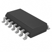
Package Options Include Plastic
Small-Outline (D) Packages and Standard
Plastic 300-mil DIPs (N)
1
14
2
13
3
12
4
11
5
10
6
9
7
8
C
D
E
VCC
F
G
H
description
The 74ACT11286 universal 9-bit parity generator/checker features a local output for parity checking and a
bus-driving parity I/O port for parity generation/checking. The word-length capability is easily expanded by
cascading.
The XMIT control input is implemented specifically to accommodate cascading. When the XMIT is low, the parity
tree is disabled and the PARITY ERROR output remains at a high logic level, regardless of the input levels.
When XMIT is high, the parity tree is enabled. PARITY ERROR indicates a parity error when either an even
number of inputs (A through I) are high and PARITY I/O is forced to a low logic level, or when an odd number
of inputs are high and PARITY I/O is forced to a high logic level.
The I/O control circuitry is designed so that the I/O port remains in the high-impedance state during power up
or power down, to prevent bus glitches.
The 74ACT11286 is characterized for operation from −40°C to 85°C.
FUNCTION TABLE
NUMBER OF INPUTS
(A−I ) THAT
ARE HIGH
XMIT
INPUT
PARITY
I/O
PARITY
ERROR
OUTPUT
0, 2, 4, 6, 8
l
H
H
1, 3, 5, 7, 9
l
L
H
h
h
H
h
l
L
h
h
L
h
l
H
0, 2, 4, 6, 8
1, 3, 5, 7, 9
h = high input level, H = high output level, I = low input level,
L = low output level
Please be aware that an important notice concerning availability, standard warranty, and use in critical applications of
Texas Instruments semiconductor products and disclaimers thereto appears at the end of this data sheet.
EPIC is a trademark of Texas Instruments Incorporated.
Copyright 1996, Texas Instruments Incorporated
�������
�� ���� ���!"#$%�!� �& '("")�% $& !� *(+,�'$%�!� -$%).
�"!-('%& '!��!"# %! &*)'���'$%�!�& *)" %/) %)"#& !� �)0$&
�&%"(#)�%&
&%$�-$"- 1$""$�%2. �"!-('%�!� *"!')&&��3 -!)& �!% �)')&&$"�,2 ��',(-)
%)&%��3 !� $,, *$"$#)%)"&.
•
POST OFFICE BOX 655303 DALLAS, TEXAS 75265
POST OFFICE BOX 1443 HOUSTON, TEXAS 77251−1443
•
1
����������
��
� ���
�� �����������������
�
�� ��� ��
��� ���
��
�� �����
SCAS069B − AUGUST 1988 − REVISED APRIL 1996
logic symbol†
A
B
C
D
E
F
G
H
I
XMIT
2
2k
1
14
13
1
12
3
PARITY I/O
N2
10
9
8
2, 1
7
6
5
PARITY ERROR
EN 1
† This symbol is in accordance with ANSI/IEEE Std 91-1984 and IEC Publication 617-12.
logic diagram (positive logic)
A
B
C
D
E
F
G
H
I
PARITY I/O
XMIT
2
2
1
14
13
12
10
5 PARITY
ERROR
9
8
7
3
6
•
POST OFFICE BOX 655303 DALLAS, TEXAS 75265
POST OFFICE BOX 1443 HOUSTON, TEXAS 77251−1443
•
����������
��
� ���
�� �����������������
�
�� ��� ��
��� ���
��
�� �����
SCAS069B − AUGUST 1988 − REVISED APRIL 1996
absolute maximum ratings over operating free-air temperature range (unless otherwise noted)†
Supply voltage range, VCC . . . . . . . . . . . . . . . . . . . . . . . . . . . . . . . . . . . . . . . . . . . . . . . . . . . . . . . . . . −0.5 V to 7 V
Input voltage range, VI (see Note 1) . . . . . . . . . . . . . . . . . . . . . . . . . . . . . . . . . . . . . . . . . . . . −0.5 V to VCC + 0.5 V
Output voltage range, VO (see Note 1) . . . . . . . . . . . . . . . . . . . . . . . . . . . . . . . . . . . . . . . . . −0.5 V to VCC + 0.5 V
Input clamp current, IIK (VI < 0 or VI > VCC) . . . . . . . . . . . . . . . . . . . . . . . . . . . . . . . . . . . . . . . . . . . . . . . . . ±20 mA
Output clamp current, IOK (VO < 0 or VO > VCC) . . . . . . . . . . . . . . . . . . . . . . . . . . . . . . . . . . . . . . . . . . . . ±50 mA
Continuous output current, IO (VO = 0 to VCC) . . . . . . . . . . . . . . . . . . . . . . . . . . . . . . . . . . . . . . . . . . . . . . ±50 mA
Continuous current through VCC or GND . . . . . . . . . . . . . . . . . . . . . . . . . . . . . . . . . . . . . . . . . . . . . . . . . . ±100 mA
Maximum power dissipation at TA = 55°C (in still air) (see Note 2): D package . . . . . . . . . . . . . . . . . . . 1.25 W
N package . . . . . . . . . . . . . . . . . . . . 1.1 W
Storage temperature range, Tstg . . . . . . . . . . . . . . . . . . . . . . . . . . . . . . . . . . . . . . . . . . . . . . . . . . . . −65°C to 150°C
† Stresses beyond those listed under “absolute maximum ratings” may cause permanent damage to the device. These are stress ratings only, and
functional operation of the device at these or any other conditions beyond those indicated under “recommended operating conditions” is not
implied. Exposure to absolute-maximum-rated conditions for extended periods may affect device reliability.
NOTES: 1. The input and output voltage ratings may be exceeded if the input and output current ratings are observed.
2. The maximum package power dissipation is calculated using a junction temperature of 150_C and a board trace length of 750 mils,
except for the N package, which has a trace length of zero.
recommended operating conditions
MIN
MAX
4.5
5.5
VCC
VIH
Supply voltage
VIL
VI
Low-level input voltage
Input voltage
0
VO
IOH
Output voltage
0
High-level input voltage
2
UNIT
V
V
0.8
V
VCC
VCC
V
High-level output current
−24
mA
IOL
Dt/Dv
Low-level output current
24
mA
0
10
ns/V
TA
Operating free-air temperature
−40
85
°C
Input transition rise or fall rate
•
POST OFFICE BOX 655303 DALLAS, TEXAS 75265
POST OFFICE BOX 1443 HOUSTON, TEXAS 77251−1443
•
V
3
����������
��
� ���
�� �����������������
�
�� ��� ��
��� ���
��
�� �����
SCAS069B − AUGUST 1988 − REVISED APRIL 1996
electrical characteristics over recommended operating free-air temperature range (unless
otherwise noted)
PARAMETER
TEST CONDITIONS
MIN
4.5 V
4.4
4.4
5.5 V
5.4
5.4
4.5 V
3.94
3.8
IOH = −24 mA
5.5 V
4.94
4.8
IOH = −75 mA†
5.5 V
IOH = −50 mA
A
VOH
IL = 50 mA
A
VOL
IOZ
II
IOL = 24 mA
PARITY I/O
Except PARITY I/O
ICC
TA = 25°C
TYP
MAX
VCC
MIN
MAX
UNIT
V
3.85
4.5 V
0.1
5.5 V
0.1
0.1
0.1
4.5 V
0.36
0.44
5.5 V
0.36
0.44
V
IOL = 75 mA†
VO = VCC or GND
5.5 V
5.5 V
±0.5
±5
mA
VI = VCC or GND
VI = VCC or GND,
5.5 V
±0.1
±1
mA
5.5 V
8
80
mA
5.5 V
0.9
1
mA
IO = 0
DICC‡
One input at 3.4 V,
Other inputs at GND or VCC
Ci
VI = VCC or GND
VO = VCC or GND
1.65
5V
3.5
pF
Co
PARITY I/O
5V
8
† Not more than one output should be tested at a time, and the duration of the test should not exceed 10 ms.
‡ This is the increase in supply current for each input that is at one of the specified TTL voltage levels rather than 0 V to VCC.
pF
switching characteristics over recomended ranges of supply voltage and operating free-air
temperature (unless otherwise noted) (see Figure 1)
PARAMETER
FROM
(INPUT)
TO
(OUTPUT)
tPLH
tPHL
Any A−I
PARITY I/O
tPLH
tPHL
Any A−I
PARITY ERROR
tPLH
tPHL
PARITY I/O
PARITY ERROR
tPZH
tPZL
XMIT
PARITY I/O
tPHZ
tPLZ
XMIT
PARITY I/O
TA = 25°C
MIN
TYP
MAX
MIN
MAX
2.7
6.1
9
2.7
10.4
3.6
7.3
10.8
3.6
12
3
6.9
9.7
3
11.3
3.9
7.7
11.4
3.9
12.9
2.2
4.6
6.8
2.2
7.7
3.1
5.6
8.3
3.1
9.1
1.8
4.2
6.3
1.8
7.3
3
6.3
9.4
3
11.4
4.7
6.5
7.9
4.7
8.5
4.1
6
7.3
4.1
7.8
UNIT
ns
ns
ns
ns
ns
operating characteristics, VCC = 5 V, TA = 25°C
PARAMETER
TEST CONDITIONS
Outputs enabled
Cpd
4
Power dissipation capacitance
Outputs disabled
•
POST OFFICE BOX 655303 DALLAS, TEXAS 75265
POST OFFICE BOX 1443 HOUSTON, TEXAS 77251−1443
•
TYP
UNIT
56
CL = 50 pF,
f = 1 MHz
50
pF
����������
��
� ���
�� �����������������
�
�� ��� ��
��� ���
��
�� �����
SCAS069B − AUGUST 1988 − REVISED APRIL 1996
PARAMETER MEASUREMENT INFORMATION
2 × VCC
500 Ω
From Output
Under Test
S1
Open
GND
CL = 50 pF
(see Note A)
500 Ω
TEST
S1
tPLH/tPHL
tPLZ/tPZL
tPHZ/tPZH
Open
2 × VCC
GND
1.5 V
1.5 V
LOAD CIRCUIT
Output
Control
(low-level
enabling)
3V
Input
1.5 V
1.5 V
0V
tPHL
tPLH
50% VCC
0V
tPZL
tPLZ
Output
Waveform 1
S1 at 2 × VCC
(see Note B)
VOH
Output
3V
Output
Waveform 2
S1 at GND
(see Note B)
50% VCC
VOL
50% VCC
[ VCC
20% VCC
VOL
tPHZ
tPZH
50% VCC
80% VCC
VOH
[0V
VOLTAGE WAVEFORMS
VOLTAGE WAVEFORMS
NOTES: A. CL includes probe and jig capacitance.
B. Waveform 1 is for an output with internal conditions such that the output is low except when disabled by the output control.
Waveform 2 is for an output with internal conditions such that the output is high except when disabled by the output control.
C. All input pulses are supplied by generators having the following characteristics: PRR ≤ 1 MHz, ZO = 50 Ω, tr = 3 ns, tf = 3 ns.
D. The outputs are measured one at a time with one transition per measurement.
Figure 1. Load Circuit and Voltage Waveforms
•
POST OFFICE BOX 655303 DALLAS, TEXAS 75265
POST OFFICE BOX 1443 HOUSTON, TEXAS 77251−1443
•
5
�PACKAGE OPTION ADDENDUM
www.ti.com
10-Dec-2020
PACKAGING INFORMATION
Orderable Device
Status
(1)
Package Type Package Pins Package
Drawing
Qty
Eco Plan
(2)
Lead finish/
Ball material
MSL Peak Temp
Op Temp (°C)
Device Marking
(3)
(4/5)
(6)
74ACT11286D
ACTIVE
SOIC
D
14
50
RoHS & Green
NIPDAU
Level-1-260C-UNLIM
-40 to 85
ACT11286
(1)
The marketing status values are defined as follows:
ACTIVE: Product device recommended for new designs.
LIFEBUY: TI has announced that the device will be discontinued, and a lifetime-buy period is in effect.
NRND: Not recommended for new designs. Device is in production to support existing customers, but TI does not recommend using this part in a new design.
PREVIEW: Device has been announced but is not in production. Samples may or may not be available.
OBSOLETE: TI has discontinued the production of the device.
(2)
RoHS: TI defines "RoHS" to mean semiconductor products that are compliant with the current EU RoHS requirements for all 10 RoHS substances, including the requirement that RoHS substance
do not exceed 0.1% by weight in homogeneous materials. Where designed to be soldered at high temperatures, "RoHS" products are suitable for use in specified lead-free processes. TI may
reference these types of products as "Pb-Free".
RoHS Exempt: TI defines "RoHS Exempt" to mean products that contain lead but are compliant with EU RoHS pursuant to a specific EU RoHS exemption.
Green: TI defines "Green" to mean the content of Chlorine (Cl) and Bromine (Br) based flame retardants meet JS709B low halogen requirements of


 工商网监
湘ICP备2023018690号
工商网监
湘ICP备2023018690号
