74F240, 74F244
Octal Buffers/Line Drivers with 3-STATE Outputs
tm
Features
General Description
■ 3-STATE outputs drive bus lines or buffer memory
The 74F240 and 74F244 are octal buffers and line drivers designed to be employed as memory and address
drivers, clock drivers and bus-oriented transmitters/
receivers which provide improved PC and board density.
address registers
■ Outputs sink 64mA (48mA mil)
■ 12mA source current
■ Input clamp diodes limit high-speed termination
effects
Ordering Information
Order Code
Package
Number
Package Description
74F240SC(1)
M20B
20-Lead Small Outline Integrated Circuit (SOIC), JEDEC MS-013, 0.300" Wide
74F240SJ(1)
M20D
20-Lead Small Outline Package (SOP), EIAJ TYPE II, 5.3mm Wide
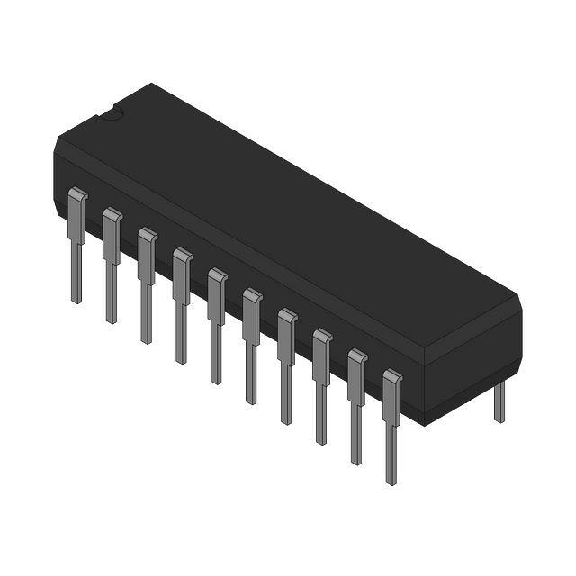
74F240PC
N20A
20-Lead Plastic Dual-In-Line Package (PDIP), JEDEC MS-001, 0.300" Wide
74F244SC(1)
M20B
20-Lead Small Outline Integrated Circuit (SOIC), JEDEC MS-013, 0.300" Wide
74F244SJ(1)
M20D
20-Lead Small Outline Package (SOP), EIAJ TYPE II, 5.3mm Wide
74F244MSA(1)
74F244PC
MSA20
N20A
20-Lead Shrink Small Outline Package (SSOP), JEDEC MO-150, 5.3mm Wide
20-Lead Plastic Dual-In-Line Package (PDIP), JEDEC MS-001, 0.300" Wide
Note:
1. Devices also available in Tape and Reel. Specify by appending the suffix letter “X” to the ordering number.
Connection Diagrams
74F240
©1988 Fairchild Semiconductor Corporation
74F240, 74F244 Rev. 1.4
74F244
www.fairchildsemi.com
74F240, 74F244 Octal Buffers/Line Drivers with 3-STATE Outputs
May 2007
�IEEE/IEC
74F244
IEEE/IEC
74F240
Unit Loading/Fan Out
Pin Names
Description
U.L.
HIGH/LOW
Input IIH / IIL,
Output IOH / IOL
OE1, OE2
3-STATE Output Enable Input (Active LOW)
1.0 / 1.667
20µA / –1mA
OE2
3-STATE Output Enable Input (Active HIGH)
1.0 / 1.667
20µA / –1mA
I0–I7
Inputs (74F240)
I0–I7
Inputs (74F244)
O0–O7, O0–O7
Outputs
1.0 /
1.667(2)
1.0 /
2.667(2)
600 / 106.6 (80)
20µA / –1mA
20µA / –1.6mA
–12mA / 64mA (48mA)
Note:
2. Worst-case 74F240 enabled; 74F244 disabled.
Truth Tables
74F240
74F244
OE1
D1n
O1n
OE2
D2n
O2n
OE1
D1n
O1n
OE2
D2n
O2n
H
X
Z
H
X
Z
H
X
Z
H
X
Z
L
H
L
L
H
L
L
H
H
L
H
H
L
L
H
L
L
H
L
L
L
L
L
L
H = HIGH Voltage Level
L = LOW Voltage Level
X = Immaterial
Z = High Impedance
©1988 Fairchild Semiconductor Corporation
74F240, 74F244 Rev. 1.4
www.fairchildsemi.com
2
74F240, 74F244 Octal Buffers/Line Drivers with 3-STATE Outputs
Logic Symbols
�Symbol
TSTG
Parameter
Rating
Storage Temperature
–65°C to +150°C
TA
Ambient Temperature Under Bias
–55°C to +125°C
TJ
Junction Temperature Under Bias
–55°C to +150°C
VCC
VCC Pin Potential to Ground Pin
–0.5V to +7.0V
VIN
Input Voltage(3)
–0.5V to +7.0V
IIN
Input Current(3)
–30mA to +5.0mA
VO
Voltage Applied to Output in HIGH State (with VCC = 0V)
Standard Output
–0.5V to VCC
3-STATE Output
–0.5V to 5.5V
Current Applied to Output in LOW State (Max.)
twice the rated IOL (mA)
ESD Last Passing Voltage (Min.)
4000V
Note:
3. Either voltage limit or current limit is sufficient to protect inputs.
Recommended Operating Conditions
The Recommended Operating Conditions table defines the conditions for actual device operation. Recommended
operating conditions are specified to ensure optimal performance to the datasheet specifications. Fairchild does not
recommend exceeding them or designing to absolute maximum ratings.
Symbol
TA
VCC
Parameter
Rating
Free Air Ambient Temperature
0°C to +70°C
Supply Voltage
©1988 Fairchild Semiconductor Corporation
74F240, 74F244 Rev. 1.4
+4.5V to +5.5V
www.fairchildsemi.com
3
74F240, 74F244 Octal Buffers/Line Drivers with 3-STATE Outputs
Absolute Maximum Ratings
Stresses exceeding the absolute maximum ratings may damage the device. The device may not function or be
operable above the recommended operating conditions and stressing the parts to these levels is not recommended.
In addition, extended exposure to stresses above the recommended operating conditions may affect device reliability.
The absolute maximum ratings are stress ratings only.
�Symbol
Parameter
VCC
Conditions
Min.
2.0
Typ.
Max.
Units
V
VIH
Input HIGH Voltage
Recognized as a HIGH Signal
VIL
Input LOW Voltage
Recognized as a LOW Signal
0.8
V
VCD
Input Clamp Diode Voltage
Min.
IIN = –18mA
–1.2
V
VOH
Output HIGH Voltage
Min.
IOH = –3mA
10% VCC
2.4
10% VCC
IOH = –15mA
2.0
5% VCC
IOH = –3mA
2.7
10% VCC
Min.
V
IOL = 64mA
VOL
Output LOW Voltage
0.55
IIH
Input HIGH Current
Max.
VIN = 2.7V
5.0
µA
IBVI
Input HIGH Current Breakdown
Test
Max.
VIN = 7.0V
7.0
µA
ICEX
Output HIGH Leakage Current
Max.
VOUT = VCC
50
µA
VID
Input Leakage Test
0.0
IID = 1.9µA
IOD
Output Leakage Circuit Current
0.0
4.75
V
V
All Other Pins Grounded
VIOD = 150mV
3.75
µA
VIN = 0.5V (OE1, OE2, OE2,
Dn (74F240))
–1.0
mA
VIN = 0.5V (Dn (74F244))
–1.6
All Other Pins Grounded
IIL
Input LOW Current
Max.
IOZH
Output Leakage Current
Max.
VOUT = 2.7V
50
µA
IOZL
Output Leakage Current
Max.
VOUT = 0.5V
–50
µA
IOS
Output Short-Circuit Current
Max.
VOUT = 0V
–225
mA
IZZ
Bus Drainage Test
0.0V
VOUT = 5.25V
500
µA
ICCH
Power Supply Current (74F240)
Max.
VO = HIGH
19
29
mA
ICCL
Power Supply Current (74F240)
Max.
VO = LOW
50
75
mA
–100
ICCZ
Power Supply Current (74F240)
Max.
VO = HIGH Z
42
63
mA
ICCH
Power Supply Current (74F244)
Max.
VO = HIGH
40
60
mA
ICCL
Power Supply Current (74F244)
Max.
VO = LOW
60
90
mA
ICCZ
Power Supply Current (74F244)
Max.
VO = HIGH Z
60
90
mA
©1988 Fairchild Semiconductor Corporation
74F240, 74F244 Rev. 1.4
www.fairchildsemi.com
4
74F240, 74F244 Octal Buffers/Line Drivers with 3-STATE Outputs
DC Electrical Characteristics
�TA = +25°C,
VCC = +5.0V,
CL = 50pF
Symbol
Parameter
TA = –55°C to +125°C, TA = 0°C to +70°C,
VCC = 5.0V,
VCC = 5.0V,
CL = 50pF
CL = 50pF
Min. Typ. Max.
Min.
Max.
Min.
Max.
Units
ns
Propagation Delay
Data to Output
(74F240)
3.0
5.1
7.0
3.0
9.0
3.0
8.0
2.0
3.5
4.7
2.0
6.0
2.0
5.7
Output Enable Time
(74F240)
2.0
3.5
4.7
2.0
6.5
2.0
5.7
4.0
6.9
9.0
4.0
10.5
4.0
10.0
tPHZ, tPLZ
Output Disable Time
(74F240)
2.0
4.0
5.3
2.0
6.5
2.0
6.3
2.0
6.0
8.0
2.0
12.5
2.0
9.5
tPLH, tPHL
Propagation Delay,
Data to Output
(74F244)
2.5
4.0
5.2
2.0
6.5
2.5
6.2
2.5
4.0
5.2
2.0
7.0
2.5
6.5
Output Enable Time
(74F244)
2.0
4.3
5.7
2.0
7.0
2.0
6.7
2.0
5.4
7.0
2.0
8.5
2.0
8.0
Output Disable Time
(74F244)
2.0
4.5
6.0
2.0
7.0
2.0
7.0
2.0
4.5
6.0
2.0
7.5
2.0
7.0
tPLH, tPHL
tPZH, tPZL
tPZH, tPZL
tPHZ, tPLZ
©1988 Fairchild Semiconductor Corporation
74F240, 74F244 Rev. 1.4
ns
ns
ns
www.fairchildsemi.com
5
74F240, 74F244 Octal Buffers/Line Drivers with 3-STATE Outputs
AC Electrical Characteristics
�74F240, 74F244 Octal Buffers/Line Drivers with 3-STATE Outputs
Physical Dimensions
Dimensions are in inches (millimeters) unless otherwise noted.
Figure 1. 20-Lead Small Outline Integrated Circuit (SOIC), JEDEC MS-013, 0.300" Wide
Package Number M20B
©1988 Fairchild Semiconductor Corporation
74F240, 74F244 Rev. 1.4
www.fairchildsemi.com
6
�74F240, 74F244 Octal Buffers/Line Drivers with 3-STATE Outputs
Physical Dimensions (Continued)
Dimensions are in millimeters unless otherwise noted.
Figure 2. 20-Lead Small Outline Package (SOP), EIAJ TYPE II, 5.3mm Wide
Package Number M20D
©1988 Fairchild Semiconductor Corporation
74F240, 74F244 Rev. 1.4
www.fairchildsemi.com
7
�74F240, 74F244 Octal Buffers/Line Drivers with 3-STATE Outputs
Physical Dimensions (Continued)
Dimensions are in millimeters unless otherwise noted.
Figure 3. 20-Lead Shrink Small Outline Package (SSOP), JEDEC MO-150, 5.3mm Wide
Package Number MSA20
©1988 Fairchild Semiconductor Corporation
74F240, 74F244 Rev. 1.4
www.fairchildsemi.com
8
�74F240, 74F244 Octal Buffers/Line Drivers with 3-STATE Outputs
Physical Dimensions (Continued)
Dimensions are in inches (millimeters) unless otherwise noted.
Figure 4. 20-Lead Plastic Dual-In-Line Package (PDIP), JEDEC MS-001, 0.300" Wide
Package Number N20A
©1988 Fairchild Semiconductor Corporation
74F240, 74F244 Rev. 1.4
www.fairchildsemi.com
9
�®
ACEx
Across the board. Around the world.™
ActiveArray™
Bottomless™
Build it Now™
CoolFET™
CROSSVOLT™
CTL™
Current Transfer Logic™
DOME™
2
E CMOS™
®
EcoSPARK
EnSigna™
FACT Quiet Series™
®
FACT
®
FAST
FASTr™
FPS™
®
FRFET
GlobalOptoisolator™
GTO™
HiSeC™
i-Lo™
ImpliedDisconnect™
IntelliMAX™
ISOPLANAR™
MICROCOUPLER™
MicroPak™
MICROWIRE™
Motion-SPM™
MSX™
MSXPro™
OCX™
OCXPro™
®
OPTOLOGIC
®
OPTOPLANAR
PACMAN™
PDP-SPM™
POP™
®
Power220
®
Power247
PowerEdge™
PowerSaver™
Power-SPM™
®
PowerTrench
Programmable Active Droop™
®
QFET
QS™
QT Optoelectronics™
Quiet Series™
RapidConfigure™
RapidConnect™
ScalarPump™
SMART START™
®
SPM
STEALTH™
SuperFET™
SuperSOT™-3
SuperSOT™-6
SuperSOT™-8
SyncFET™
TCM™
®
The Power Franchise
TinyBoost™
TinyBuck™
®
TinyLogic
TINYOPTO™
TinyPower™
TinyWire™
TruTranslation™
µSerDes™
®
UHC
UniFET™
VCX™
Wire™
™
DISCLAIMER
FAIRCHILD SEMICONDUCTOR RESERVES THE RIGHT TO MAKE CHANGES WITHOUT FURTHER NOTICE TO ANY PRODUCTS
HEREIN TO IMPROVE RELIABILITY, FUNCTION OR DESIGN. FAIRCHILD DOES NOT ASSUME ANY LIABILITY ARISING OUT OF THE
APPLICATION OR USE OF ANY PRODUCT OR CIRCUIT DESCRIBED HEREIN; NEITHER DOES IT CONVEY ANY LICENSE UNDER
ITS PATENT RIGHTS, NOR THE RIGHTS OF OTHERS. THESE SPECIFICATIONS DO NOT EXPAND THE TERMS OF FAIRCHILD’S
WORLDWIDE TERMS AND CONDITIONS, SPECIFICALLY THE WARRANTY THEREIN, WHICH COVERS THESE PRODUCTS.
LIFE SUPPORT POLICY
FAIRCHILD’S PRODUCTS ARE NOT AUTHORIZED FOR USE AS CRITICAL COMPONENTS IN LIFE SUPPORT DEVICES OR
SYSTEMS WITHOUT THE EXPRESS WRITTEN APPROVAL OF FAIRCHILD SEMICONDUCTOR CORPORATION.
As used herein:
1. Life support devices or systems are devices or systems
which, (a) are intended for surgical implant into the body or
(b) support or sustain life, and (c) whose failure to perform
when properly used in accordance with instructions for use
provided in the labeling, can be reasonably expected to
result in a significant injury of the user.
2. A critical component in any component of a life support,
device, or system whose failure to perform can be
reasonably expected to cause the failure of the life support
device or system, or to affect its safety or effectiveness.
PRODUCT STATUS DEFINITIONS
Definition of Terms
Datasheet Identification
Product Status
Advance Information
Formative or In Design
This datasheet contains the design specifications for product
development. Specifications may change in any manner without notice.
Definition
Preliminary
First Production
This datasheet contains preliminary data; supplementary data will be
published at a later date. Fairchild Semiconductor reserves the right to
make changes at any time without notice to improve design.
No Identification Needed
Full Production
This datasheet contains final specifications. Fairchild Semiconductor
reserves the right to make changes at any time without notice to improve
design.
Obsolete
Not In Production
This datasheet contains specifications on a product that has been
discontinued by Fairchild Semiconductor. The datasheet is printed for
reference information only.
Rev. I26
©1988 Fairchild Semiconductor Corporation
74F240, 74F244 Rev. 1.4
www.fairchildsemi.com
10
74F240, 74F244 Octal Buffers/Line Drivers with 3-STATE Outputs
TRADEMARKS
The following are registered and unregistered trademarks Fairchild Semiconductor owns or is authorized to use and is not intended to be an
exhaustive list of all such trademarks.
�


 工商网监
湘ICP备2023018690号
工商网监
湘ICP备2023018690号
