OBSOLETE
ADC08031, ADC08032, ADC08034, ADC08038
www.ti.com
SNAS062C – JUNE 1999 – REVISED APRIL 2013
ADC08031/ADC08032/ADC08034/ADC08038 8-Bit High-Speed Serial I/O A/D Converters
with Multiplexer Options, Voltage Reference, and Track/Hold Function
Check for Samples: ADC08031, ADC08032, ADC08034, ADC08038
FEATURES
KEY SPECIFICATIONS
•
•
•
•
•
•
•
•
•
1
2
•
•
•
•
•
•
Serial Digital Data Link Requires Few I/O Pins
Analog Input Track/Hold Function
2-, 4-, or 8-Channel Input Multiplexer Options
with Address Logic
0V to 5V Analog Input Range with Single 5V
Power Supply
No Zero or Full Scale Adjustment Required
TTL/CMOS Input/Output Compatible
On Chip 2.6V Band-Gap Reference
0.3″ Standard Width 8-, 14-, or 20-Pin PDIP
Package
14-, 20-Pin Small-Outline Packages
APPLICATIONS
•
•
•
•
•
•
Digitizing Automotive Sensors
Process Control Monitoring
Remote Sensing in Noisy Environments
Instrumentation
Test Systems
Embedded Diagnostics
Resolution: 8 bits
Conversion time (fC = 1 MHz): 8 μs (max)
Power dissipation: 20 mW (max)
Single supply: 5VDC (±5%)
Total unadjusted error: ±½ LSB and ±1LSB
No missing codes over temperature
DESCRIPTION
The
ADC08031/ADC08032/ADC08034/ADC08038
are 8-bit successive approximation A/D converters
with serial I/O and configurable input multiplexers with
up to 8 channels. The serial I/O is configured to
comply with the NSC MICROWIRE serial data
exchange standard for easy interface to the COPS
family of controllers, and can easily interface with
standard shift registers or microprocessors.
The ADC08034 and ADC08038 provide a 2.6V bandgap derived reference. For devices offering specific
voltage reference performance over temperature see
ADC08131, ADC08134 and ADC08138.
A track/hold function allows th e analog voltage at the
positive input to vary during the actual A/D
conversion.
The analog inputs can be configured to operate in
various combinations of single-ended, differential, or
pseudo-differential modes. In addition, input voltage
spans as small as 1V can be accommodated.
1
2
Please be aware that an important notice concerning availability, standard warranty, and use in critical applications of
Texas Instruments semiconductor products and disclaimers thereto appears at the end of this data sheet.
All trademarks are the property of their respective owners.
PRODUCTION DATA information is current as of publication date.
Products conform to specifications per the terms of the Texas
Instruments standard warranty. Production processing does not
necessarily include testing of all parameters.
Copyright © 1999–2013, Texas Instruments Incorporated
�OBSOLETE
ADC08031, ADC08032, ADC08034, ADC08038
SNAS062C – JUNE 1999 – REVISED APRIL 2013
www.ti.com
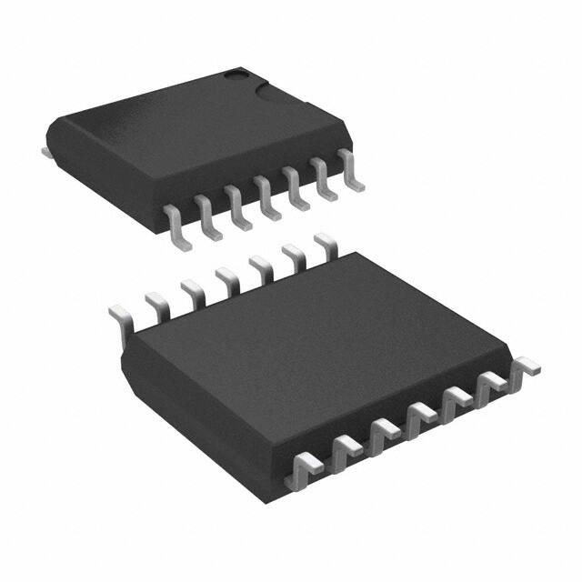
CONNECTION DIAGRAMS
Figure 1. ADC08038
SOIC and PDIP Packages
See Package Number DW and NFH
Figure 2. ADC08034 - SOIC
See Package Number NPA
Figure 3. ADC08031
Dual-In-Line Package - PDIP
See Package Number P
Figure 4. ADC08032
Small Outline Package - SOIC
See Package Number NPA
Figure 5. ADC08031
Small Outline Package - SOIC
See Package Number NPA
These devices have limited built-in ESD protection. The leads should be shorted together or the device placed in conductive foam
during storage or handling to prevent electrostatic damage to the MOS gates.
2
Submit Documentation Feedback
Copyright © 1999–2013, Texas Instruments Incorporated
Product Folder Links: ADC08031 ADC08032 ADC08034 ADC08038
�OBSOLETE
ADC08031, ADC08032, ADC08034, ADC08038
www.ti.com
SNAS062C – JUNE 1999 – REVISED APRIL 2013
ABSOLUTE MAXIMUM RATINGS (1) (2) (3)
Supply Voltage (VCC)
6.5V
−0.3V to VCC +
0.3V
Voltage at Inputs and Outputs
Input Current at Any Pin (4)
Package Input Current
±5 mA
(4)
±20 mA
Power Dissipation at A = 25°C (5)
800 mW
ESD Susceptibility (6)
1500V
Soldering Information
PDIP Package (10 sec.)
SOIC Package:
235°C
Vapor Phase (60 sec.)
215°C
Infrared (15 sec.)
220°C
−65°C to +150°C
Storage Temperature
(1)
(2)
(3)
(4)
(5)
(6)
All voltages are measured with respect to AGND = DGND = 0 VDC, unless otherwise specified.
Absolute Maximum Ratings indicate limits beyond which damage to the device may occur.
If Military/Aerospace specified devices are required, please contact the Texas Instruments Sales Office/ Distributors for availability and
specifications.
When the input voltage VIN at any pin exceeds the power supplies (VIN < (AGND or DGND) or VIN > VCC) the current at that pin should
be limited to 5 mA. The 20 mA maximum package input current rating limits the number of pins that can safely exceed the power
supplies with an input current of 5 mA to four pins.
The maximum power dissipation must be derated at elevated temperatures and is dictated by TJMAX, θJA and the ambient temperature,
TA. The maximum allowable power dissipation at any temperature is PD = (TJMAX − TA)/θJA or the number given in the Absolute
Maximum Ratings, whichever is lower. For these devices, TJMAX = 125°C. The typical thermal resistances (θJA) of these parts when
board mounted follow: ADC08031 and ADC08032 with BIN and CIN suffixes 120°C/W, ADC08038 with CIN suffix 80°C/W. ADC08031
with CIWM suffix 140°C/W, ADC08032 140°C/W, ADC08034 140°C/W, ADC08038 with CIWM suffix 91°C/W.
Human body model, 100 pF capacitor discharged through a 1.5 kΩ resistor.
OPERATING RATINGS (1) (2)
Temperature Range (TMIN ≤ TA ≤ TMAX)
ADC08031BIN, ADC08031CIN,
ADC08032BIN, ADC08032CIN,
ADC08034BIN, ADC08034CIN,
ADC08038BIN, ADC08038CIN,
ADC08031BIWM, ADC08032BIWM,
ADC08034BIWM, ADC08038BIWM,
ADC08031CIWM, ADC08032CIWM,
ADC08034CIWM, ADC08038CIWM
−40°C ≤ TA ≤ +85°C
Supply Voltage (VCC)
(1)
(2)
4.5 VDC to 6.3 VDC
Operating Ratings indicate conditions for which the device is functional. These ratings do not ensure specific performance limits. For
ensured specifications and test conditions, see the Electrical Characteristics. The ensured specifications apply only for the test
conditions listed. Some performance characteristics may degrade when the device is not operated under the listed test conditions.
All voltages are measured with respect to AGND = DGND = 0 VDC, unless otherwise specified.
Copyright © 1999–2013, Texas Instruments Incorporated
Submit Documentation Feedback
Product Folder Links: ADC08031 ADC08032 ADC08034 ADC08038
3
�OBSOLETE
ADC08031, ADC08032, ADC08034, ADC08038
SNAS062C – JUNE 1999 – REVISED APRIL 2013
www.ti.com
ELECTRICAL CHARACTERISTICS
The following specifications apply for VCC = VREF = +5 VDC, and fCLK = 1 MHz unless otherwise specified. Boldface limits
apply for TA = TJ = TMIN to TMAX; all other limits TA = TJ = 25°C.
Limits (2)
Units
(Limits)
BIN, BIWM
±½
LSB (max)
CIN, CIWM
±1
LSB (max)
Differential
8
Bits (min)
Symbol
Parameter
Conditions
Typical (1)
CONVERTER AND MULTIPLEXER CHARACTERISTICS
Total Unadjusted Error
See (3)
Linearity
RREF
VIN
Reference Input Resistance
Analog Input Voltage
See (4)
See (5)
3.5
kΩ
1.3
kΩ (min)
6.0
kΩ (max)
(VCC + 0.05)
(GND − 0.05)
V (max)
V (min)
±¼
LSB (max)
±¼
LSB (max)
μA (max)
DC Common-Mode Error
Power Supply Sensitivity
VCC = 5V ±5%,
VREF = 4.75V
On Channel Leakage
On Channel = 5V,
0.2
Current (6)
Off Channel = 0V
1
On Channel = 0V,
−0.2
Off Channel = 5V
−1
Off Channel Leakage
On Channel = 5V,
−0.2
Current (6)
Off Channel = 0V
−1
On Channel = 0V,
0.2
Off Channel = 5V
1
μA (max)
μA (max)
μA (max)
DIGITAL AND DC CHARACTERISTICS
VIN(1)
Logical “1” Input Voltage
VCC = 5.25V
2.0
VIN(0)
Logical “0” Input Voltage
VCC = 4.75V
0.8
V (max)
IIN(1)
Logical “1” Input Current
VIN = 5.0V
1
μA (max)
IIN(0)
Logical “0” Input Current
VIN = 0V
−1
μA (max)
VOUT(1)
Logical “1” Output Voltage
VCC = 4.75V:
IOUT = −360 μA
2.4
V (min)
IOUT = −10 μA
4.5
V (min)
VCC = 4.75V
0.4
V (max)
VOUT = 0V
−3.0
μA (max)
VOUT = 5V
3.0
μA (max)
VOUT(0)
Logical “0” Output Voltage
IOUT
TRI-STATE Output Current
V (min)
IOUT = 1.6 mA
(1)
(2)
(3)
(4)
(5)
(6)
4
Typical figures are at TJ = 25°C and represent the most likely parametric norm.
Specified to AOQL (Average Outgoing Quality Level).
Total unadjusted error includes offset, full-scale, linearity, multiplexer.
Cannot be tested for the ADC08032.
For VIN(−) ≥ VIN(+) the digital code will be 0000 0000. Two on-chip diodes are tied to each analog input (see Block Diagram) which will
forward-conduct for analog input voltages one diode drop below ground or one diode drop greater than VCC supply. During testing at low
VCC levels (e.g., 4.5V), high level analog inputs (e.g., 5V) can cause an input diode to conduct, especially at elevated temperatures,
which will cause errors for analog inputs near full-scale. The spec allows 50 mV forward bias of either diode; this means that as long as
the analog VIN does not exceed the supply voltage by more than 50 mV, the output code will be correct. Exceeding this range on an
unselected channel will corrupt the reading of a selected channel. Achievement of an absolute 0 VDC to 5 VDC input voltage range will
therefore require a minimum supply voltage of 4.950 VDC over temperature variations, initial tolerance and loading.
Channel leakage current is measured after a single-ended channel is selected and the clock is turned off. For off channel leakage
current the following two cases are considered: one, with the selected channel tied high (5 VDC) and the remaining seven off channels
tied low (0 VDC), total current flow through the off channels is measured; two, with the selected channel tied low and the off channels
tied high, total current flow through the off channels is again measured. The two cases considered for determining on channel leakage
current are the same except total current flow through the selected channel is measured.
Submit Documentation Feedback
Copyright © 1999–2013, Texas Instruments Incorporated
Product Folder Links: ADC08031 ADC08032 ADC08034 ADC08038
�OBSOLETE
ADC08031, ADC08032, ADC08034, ADC08038
www.ti.com
SNAS062C – JUNE 1999 – REVISED APRIL 2013
ELECTRICAL CHARACTERISTICS (continued)
The following specifications apply for VCC = VREF = +5 VDC, and fCLK = 1 MHz unless otherwise specified. Boldface limits
apply for TA = TJ = TMIN to TMAX; all other limits TA = TJ = 25°C.
Symbol
Parameter
Conditions
Typical (1)
Limits (2)
Units
(Limits)
ISOURCE
Output Source Current
VOUT = 0V
−6.5
mA (min)
ISINK
Output Sink Current
VOUT = VCC
8.0
mA (min)
ICC
Supply Current
ADC08031, ADC08034,
CS = HIGH
mA (max)
and ADC08038
3.0
ADC08032 (7)
7.0
mA (max)
REFERENCE CHARACTERISTICS
VREFOUT
Nominal Reference Output
VREFOUT Option
Available Only on
2.6
V
ADC08034 and
ADC08038
(7)
For the ADC08032 VREFIN is internally tied to VCC, therefore, for the ADC08032 reference current is included in the supply current.
ELECTRICAL CHARACTERISTICS
The following specifications apply for VCC = VREF = +5 VDC, and tr = tf = 20 ns unless otherwise specified. Boldface limits
apply for TA = TJ = TMIN to TMAX; all other limits TA = TJ = 25°C.
Symbol
fCLK
Parameter
Conditions
Clock Frequency
Typical (1)
See
Units
(Limits)
1
MHz (max)
40
% (min)
10
Clock Duty Cycle
TC
Limits (2)
(3)
Conversion Time (Not Including
fCLK = 1 MHz
kHz (min)
60
% (max)
8
1/fCLK (max)
MUX Addressing Time)
8
μs (max)
tCA
Acquisition Time
½
1/fCLK(max)
tSELECT
CLK High while CS is High
tSET-UP
CS Falling Edge or Data Input
25
ns (min)
20
ns (min)
Data MSB First
250
ns (max)
Data LSB First
200
ns (max)
50
ns
Valid to CLK Rising Edge
tHOLD
Data Input Valid after CLK
Rising Edge
tpd1, tpd0
CLK Falling Edge to Output
Data Valid
t1H, t0H
(4)
CL = 100 pF:
TRI-STATE Delay from Rising Edge
CL = 10 pF, RL = 10 kΩ
of CS to Data Output and SARS Hi-Z
(see TRI-STATE Test Circuits)
50
CL = 100 pF, RL = 2 kΩ
ns
180
ns (max)
CIN
Capacitance of Logic Inputs
5
pF
COUT
Capacitance of Logic Outputs
5
pF
(1)
(2)
(3)
(4)
Typical figures are at TJ = 25°C and represent the most likely parametric norm.
Specified to AOQL (Average Outgoing Quality Level).
A 40% to 60% duty cycle range insures proper operation at all clock frequencies. In the case that an available clock has a duty cycle
outside of these limits the minimum time the clock is high or low must be at least 450 ns. The maximum time the clock can be high or
low is 100 μs.
Since data, MSB first, is the output of the comparator used in the successive approximation loop, an additional delay is built in (see
Block Diagram) to allow for comparator response time.
Copyright © 1999–2013, Texas Instruments Incorporated
Submit Documentation Feedback
Product Folder Links: ADC08031 ADC08032 ADC08034 ADC08038
5
�OBSOLETE
ADC08031, ADC08032, ADC08034, ADC08038
SNAS062C – JUNE 1999 – REVISED APRIL 2013
www.ti.com
TYPICAL PERFORMANCE CHARACTERISTICS
Linearity Error vs.
Reference Voltage
Linearity Error vs.
Temperature
Figure 6.
Figure 7.
Linearity Error vs.
Clock Frequency
Power Supply Current vs.
Temperature (ADC08038,
ADC08034, ADC08031)
Figure 8.
6
Note: For ADC08032 add IREF
Figure 9.
Output Current vs.
Temperature
Power Supply Current
vs. Clock Frequency
Figure 10.
Figure 11.
Submit Documentation Feedback
Copyright © 1999–2013, Texas Instruments Incorporated
Product Folder Links: ADC08031 ADC08032 ADC08034 ADC08038
�OBSOLETE
ADC08031, ADC08032, ADC08034, ADC08038
www.ti.com
SNAS062C – JUNE 1999 – REVISED APRIL 2013
LEAKAGE CURRENT TEST CIRCUIT
TRI-STATE TEST CIRCUITS AND WAVEFORMS
t1H
t0H
Copyright © 1999–2013, Texas Instruments Incorporated
Submit Documentation Feedback
Product Folder Links: ADC08031 ADC08032 ADC08034 ADC08038
7
�OBSOLETE
ADC08031, ADC08032, ADC08034, ADC08038
SNAS062C – JUNE 1999 – REVISED APRIL 2013
www.ti.com
TIMING DIAGRAMS
Figure 12. Data Input Timing
*To reset these devices, CLK and CS must be simultaneously high for a period of tSELECT or greater. Otherwise these
devices are compatible with industry standards ADC0831/2/4/8.
Figure 13. Data Output Timing
Figure 14. ADC08031 Start Conversion Timing
Figure 15. ADC08031 Timing
*LSB first output not available on ADC08031.
LSB information is maintained for remainder of clock periods until CS goes high.
8
Submit Documentation Feedback
Copyright © 1999–2013, Texas Instruments Incorporated
Product Folder Links: ADC08031 ADC08032 ADC08034 ADC08038
�OBSOLETE
ADC08031, ADC08032, ADC08034, ADC08038
www.ti.com
SNAS062C – JUNE 1999 – REVISED APRIL 2013
Figure 16. ADC08032 Timing
Figure 17. ADC08034 Timing
Figure 18. ADC08038 Timing
*Make sure clock edge #18 clocks in the LSB before SE is taken low
Copyright © 1999–2013, Texas Instruments Incorporated
Submit Documentation Feedback
Product Folder Links: ADC08031 ADC08032 ADC08034 ADC08038
9
�OBSOLETE
ADC08031, ADC08032, ADC08034, ADC08038
SNAS062C – JUNE 1999 – REVISED APRIL 2013
www.ti.com
ADC08038 FUNCTIONAL BLOCK DIAGRAM
*Some of these functions/pins are not available with other options.
For the ADC08034, the “SEL 1” Flip-Flop is bypassed, for the ADC08032, both “SEL 0” and “SEL 1” Flip-Flops are
bypassed.
10
Submit Documentation Feedback
Copyright © 1999–2013, Texas Instruments Incorporated
Product Folder Links: ADC08031 ADC08032 ADC08034 ADC08038
�OBSOLETE
ADC08031, ADC08032, ADC08034, ADC08038
www.ti.com
SNAS062C – JUNE 1999 – REVISED APRIL 2013
FUNCTIONAL DESCRIPTION
MULTIPLEXER ADDRESSING
The design of these converters utilizes a comparator structure with built-in sample-and-hold which provides for a
differential analog input to be converted by a successive-approximation routine.
The actual voltage converted is always the difference between an assigned “+” input terminal and a “−” input
terminal. The polarity of each input terminal of the pair indicates which line the converter expects to be the most
positive. If the assigned “+” input voltage is less than the “−” input voltage the converter responds with an all
zeros output code.
A unique input multiplexing scheme has been utilized to provide multiple analog channels with softwareconfigurable single-ended, differential, or pseudo-differential (which will convert the difference between the
voltage at any analog input and a common terminal) operation. The analog signal conditioning required in
transducer-based data acquisition systems is significantly simplified with this type of input flexibility. One
converter package can now handle ground referenced inputs and true differential inputs as well as signals with
some arbitrary reference voltage.
A particular input configuration is assigned during the MUX addressing sequence, prior to the start of a
conversion. The MUX address selects which of the analog inputs are to be enabled and whether this input is
single-ended or differential. Differential inputs are restricted to adjacent channel pairs. For example, channel 0
and channel 1 may be selected as a differential pair but channel 0 or 1 cannot act differentially with any other
channel. In addition to selecting differential mode the polarity may also be selected. Channel 0 may be selected
as the positive input and channel 1 as the negative input or vice versa. This programmability is best illustrated by
the MUX addressing codes shown in the following tables for the various product options.
The MUX address is shifted into the converter via the DI line. Because the ADC08031 contains only one
differential input channel with a fixed polarity assignment, it does not require addressing.
The common input line (COM) on the ADC08038 can be used as a pseudo-differential input. In this mode the
voltage on this pin is treated as the “−” input for any of the other input channels. This voltage does not have to be
analog ground; it can be any reference potential which is common to all of the inputs. This feature is most useful
in single-supply applications where the analog circuity may be biased up to a potential other than ground and the
output signals are all referred to this potential.
Table 1. Multiplexer/Package Options
Number of Analog Channels
Part Number
Number of Package Pins
Single-Ended
Differential
ADC08031
1
1
ADC08032
2
1
8
ADC08034
4
2
14
ADC08038
8
4
20
8
Table 2. MUX Addressing: ADC08038
Single-Ended MUX Mode
MUX Address
Analog Single-Ended Channel #
SELECT
START
SGL/ DIF
ODD/
SIGN
1
0
1
1
0
0
0
1
1
0
0
1
1
1
0
1
0
1
1
0
1
1
1
1
1
0
0
1
1
1
0
1
1
1
1
1
0
1
1
1
1
1
Copyright © 1999–2013, Texas Instruments Incorporated
0
1
2
3
4
5
6
7
COM
−
+
−
+
−
+
−
+
−
+
−
+
−
+
+
Submit Documentation Feedback
Product Folder Links: ADC08031 ADC08032 ADC08034 ADC08038
−
11
�OBSOLETE
ADC08031, ADC08032, ADC08034, ADC08038
SNAS062C – JUNE 1999 – REVISED APRIL 2013
www.ti.com
Table 3. MUX Addressing: ADC08038
Differential MUX Mode
MUX Address
SGL/ DIF
START
Analog Differential Channel-Pair #
ODD/ SIGN
SELECT
0
1
1
0
0
1
+
−
1
0
0
0
0
1
0
0
0
1
1
0
0
1
0
1
0
0
1
1
1
0
1
0
0
1
0
1
0
1
1
0
1
1
0
1
0
1
1
1
−
2
2
3
+
−
3
4
5
+
−
6
7
+
−
−
+
+
−
+
−
+
Table 4. MUX Addressing: ADC08034
Single-Ended MUX Mode
MUX Address
START
SGL/ DIF
Channel #
ODD/ SIGN
SELECT
1
1
1
0
0
1
1
0
1
1
1
1
0
1
1
1
1
0
1
2
3
+
+
+
+
COM is internally tied to AGND
Table 5. MUX Addressing:
ADC08032
Single-Ended MUX Mode
MUX Address
Channel #
START
SGL/ DIF
ODD/ SIGN
0
1
1
0
+
1
1
1
1
+
COM is internally tied to AGND
Differential MUX Mode
MUX Address
START
SGL/ DIF
Channel #
ODD/ SIGN
SELECT
1
1
0
0
0
1
0
0
1
1
0
1
0
1
0
1
1
0
1
+
−
−
+
2
3
+
−
−
+
Differential MUX Mode
MUX Address
12
Channel #
START
SGL/ DIF
ODD/ SIGN
0
1
1
0
0
+
−
1
0
1
−
+
Submit Documentation Feedback
Copyright © 1999–2013, Texas Instruments Incorporated
Product Folder Links: ADC08031 ADC08032 ADC08034 ADC08038
�OBSOLETE
ADC08031, ADC08032, ADC08034, ADC08038
www.ti.com
SNAS062C – JUNE 1999 – REVISED APRIL 2013
Since the input configuration is under software control, it can be modified as required before each conversion. A
channel can be treated as a single-ended, ground referenced input for one conversion; then it can be
reconfigured as part of a differential channel for another conversion. Figure 19 illustrates the input flexibility which
can be achieved.
The analog input voltages for each channel can range from 50mV below ground to 50mV above VCC (typically
5V) without degrading conversion accuracy.
THE DIGITAL INTERFACE
A most important characteristic of these converters is their serial data link with the controlling processor. Using a
serial communication format offers two very significant system improvements; it allows many functions to be
included in a small package and it can eliminate the transmission of low level analog signals by locating the
converter right at the analog sensor; transmitting highly noise immune digital data back to the host processor.
To understand the operation of these converters it is best to refer to the Timing Diagrams and Functional Block
Diagram and to follow a complete conversion sequence. For clarity a separate timing diagram is shown for each
device.
1. A conversion is initiated by pulling the CS (chip select) line low. This line must be held low for the entire
conversion. The converter is now waiting for a start bit and its MUX assignment word.
2. On each rising edge of the clock the status of the data in (DI) line is clocked into the MUX address shift
register. The start bit is the first logic “1” that appears on this line (all leading zeros are ignored). Following
the start bit the converter expects the next 2 to 4 bits to be the MUX assignment word.
3. When the start bit has been shifted into the start location of the MUX register, the input channel has been
assigned and a conversion is about to begin. An interval of ½ clock period (where nothing happens) is
automatically inserted to allow the selected MUX channel to settle. The SARS line goes high at this time to
signal that a conversion is now in progress and the DI line is disabled (it no longer accepts data).
4. The data out (DO) line now comes out of TRI-STATE and provides a leading zero for this one clock period of
MUX settling time.
5. During the conversion the output of the SAR comparator indicates whether the analog input is greater than
(high) or less than (low) a series of successive voltages generated internally from a ratioed capacitor array
(first 5 bits) and a resistor ladder (last 3 bits). After each comparison the comparator's output is shipped to
the DO line on the falling edge of CLK. This data is the result of the conversion being shifted out (with the
MSB first) and can be read by the processor immediately.
6. After 8 clock periods the conversion is completed. The SARS line returns low to indicate this ½ clock cycle
later.
7. The stored data in the successive approximation register is loaded into an internal shift register. If the
programmer prefers the data can be provided in an LSB first format [this makes use of the shift enable (SE)
control line]. On the ADC08038 the SE line is brought out and if held high the value of the LSB remains valid
on the DO line. When SE is forced low the data is clocked out LSB first. On devices which do not include the
SE control line, the data, LSB first, is automatically shifted out the DO line after the MSB first data stream.
The DO line then goes low and stays low until CS is returned high. The ADC08031 is an exception in that its
data is only output in MSB first format.
8. All internal registers are cleared when the CS line is high and the tSELECT requirement is met. See Data Input
Timing under Timing Diagrams. If another conversion is desired CS must make a high to low transition
followed by address information.
– The DI and DO lines can be tied together and controlled through a bidirectional processor I/O bit with one
wire. This is possible because the DI input is only “looked-at” during the MUX addressing interval while
the DO line is still in a high impedance state.
Copyright © 1999–2013, Texas Instruments Incorporated
Submit Documentation Feedback
Product Folder Links: ADC08031 ADC08032 ADC08034 ADC08038
13
�OBSOLETE
ADC08031, ADC08032, ADC08034, ADC08038
SNAS062C – JUNE 1999 – REVISED APRIL 2013
www.ti.com
8 Single-Ended
8 Pseudo-Differential
4 Differential
Mixed Mode
Figure 19. Analog Input Multiplexer Options for the ADC08038
REFERENCE CONSIDERATIONS
The voltage applied to the reference input on these converters, VREFIN, defines the voltage span of the analog
input (the difference between VIN(MAX) and VIN(MIN) over which the 256 possible output codes apply. The devices
can be used either in ratiometric applications or in systems requiring absolute accuracy. The reference pin must
be connected to a voltage source capable of driving the reference input resistance which can be as low as
1.3kΩ. This pin is the top of a resistor divider string and capacitor array used for the successive approximation
conversion.
In a ratiometric system the analog input voltage is proportional to the voltage used for the A/D reference. This
voltage is typically the system power supply, so the VREFIN pin can be tied to VCC (done internally on the
ADC08032). This technique relaxes the stability requirements of the system reference as the analog input and
A/D reference move together maintaining the same output code for a given input condition.
For absolute accuracy, where the analog input varies between very specific voltage limits, the reference pin can
be biased with a time and temperature stable voltage source. For the ADC08034 and the ADC08038 a band-gap
derived reference voltage of 2.6V (1) is tied to VREFOUT. This can be tied back to VREFIN. Bypassing VREFOUT
with a 100μF capacitor is recommended. The LM385 and LM336 reference diodes are good low current devices
to use with these converters.
The maximum value of the reference is limited to the VCC supply voltage. The minimum value, however, can be
quite small (see Typical Performance Characteristics) to allow direct conversions of transducer outputs providing
less than a 5V output span. Particular care must be taken with regard to noise pickup, circuit layout and system
error voltage sources when operating with a reduced span due to the increased sensitivity of the converter (1
LSB equals VREF/256).
(1)
14
Typical figures are at TJ = 25°C and represent the most likely parametric norm.
Submit Documentation Feedback
Copyright © 1999–2013, Texas Instruments Incorporated
Product Folder Links: ADC08031 ADC08032 ADC08034 ADC08038
�OBSOLETE
ADC08031, ADC08032, ADC08034, ADC08038
www.ti.com
SNAS062C – JUNE 1999 – REVISED APRIL 2013
a) Ratiometric
b) Absolute with a Reduced Span
Figure 20. Reference Examples
THE ANALOG INPUTS
The most important feature of these converters is that they can be located right at the analog signal source and
through just a few wires can communicate with a controlling processor with a highly noise immune serial bit
stream. This in itself greatly minimizes circuitry to maintain analog signal accuracy which otherwise is most
susceptible to noise pickup. However, a few words are in order with regard to the analog inputs should the input
be noisy to begin with or possibly riding on a large common-mode voltage.
The differential input of these converters actually reduces the effects of common-mode input noise, a signal
common to both selected “+” and “−” inputs for a conversion (60 Hz is most typical). The time interval between
sampling the “+” input and then the “−” input is ½ of a clock period. The change in the common-mode voltage
during this short time interval can cause conversion errors. For a sinusoidal common-mode signal this error is:
where
•
•
•
fCM is the frequency of the common-mode signal,
VPEAK is its peak voltage value, and
fCLK is the A/D clock frequency.
(1)
For a 60Hz common-mode signal to generate a ¼ LSB error (≈5mV) with the converter running at 250kHz, its
peak value would have to be 6.63V which would be larger than allowed as it exceeds the maximum analog input
limits.
Copyright © 1999–2013, Texas Instruments Incorporated
Submit Documentation Feedback
Product Folder Links: ADC08031 ADC08032 ADC08034 ADC08038
15
�OBSOLETE
ADC08031, ADC08032, ADC08034, ADC08038
SNAS062C – JUNE 1999 – REVISED APRIL 2013
www.ti.com
Source resistance limitation is important with regard to the DC leakage currents of the input multiplexer. Bypass
capacitors should not be used if the source resistance is greater than 1kΩ. The worst-case leakage current of
±1μA over temperature will create a 1mV input error with a 1kΩ source resistance. An op amp RC active low
pass filter can provide both impedance buffering and noise filtering should a high impedance signal source be
required.
OPTIONAL ADJUSTMENTS
Zero Error
The zero of the A/D does not require adjustment. If the minimum analog input voltage value, VIN(MIN), is not
ground a zero offset can be done. The converter can be made to output 0000 0000 digital code for this minimum
input voltage by biasing any VIN (−) input at this VIN(MIN) value. This utilizes the differential mode operation of the
A/D.
The zero error of the A/D converter relates to the location of the first riser of the transfer function and can be
measured by grounding the VIN (−) input and applying a small magnitude positive voltage to the VIN (+) input.
Zero error is the difference between the actual DC input voltage which is necessary to just cause an output
digital code transition from 0000 0000 to 0000 0001 and the ideal ½ LSB value (½ LSB = 9.8mV for VREF =
5.000VDC).
Full Scale
The full-scale adjustment can be made by applying a differential input voltage which is 1½ LSB down from the
desired analog full-scale voltage range and then adjusting the magnitude of the VREFIN input (or VCC for the
ADC08032) for a digital output code which is just changing from 1111 1110 to 1111 1111.
Adjusting for an Arbitrary Analog Input
Voltage Range
If the analog zero voltage of the A/D is shifted away from ground (for example, to accommodate an analog input
signal which does not go to ground), this new zero reference should be properly adjusted first. A VIN (+) voltage
which equals this desired zero reference plus ½ LSB (where the LSB is calculated for the desired analog span,
using 1 LSB = analog span/256) is applied to selected “+” input and the zero reference voltage at the
corresponding “−” input should then be adjusted to just obtain the 00HEX to 01HEX code transition.
The full-scale adjustment should be made [with the proper VIN (−) voltage applied] by forcing a voltage to the VIN
(+) input which is given by:
where
•
•
VMAX = the high end of the analog input range, and
VMIN = the low end (the offset zero) of the analog range.
(2)
(Both are ground referenced.)
The VREFIN (or VCC) voltage is then adjusted to provide a code change from FEHEX to FFHEX. This completes the
adjustment procedure.
16
Submit Documentation Feedback
Copyright © 1999–2013, Texas Instruments Incorporated
Product Folder Links: ADC08031 ADC08032 ADC08034 ADC08038
�OBSOLETE
ADC08031, ADC08032, ADC08034, ADC08038
www.ti.com
SNAS062C – JUNE 1999 – REVISED APRIL 2013
APPLICATIONS
Figure 21. A “Stand-Alone” Hook-Up for ADC08038 Evaluation
*Pinouts shown for ADC08038.
For all other products tie to pin functions as shown.
Figure 22. Low-Cost Remote Temperature Sensor
Copyright © 1999–2013, Texas Instruments Incorporated
Submit Documentation Feedback
Product Folder Links: ADC08031 ADC08032 ADC08034 ADC08038
17
�OBSOLETE
ADC08031, ADC08032, ADC08034, ADC08038
SNAS062C – JUNE 1999 – REVISED APRIL 2013
www.ti.com
Figure 23. Digitizing a Current Flow
Figure 24. Operating with Ratiometric Transducers
*VIN(−) = 0.15 VCC
15% of VCC ≤ VXDR ≤ 85% of VCC
Figure 25. Span Adjust; 0V ≤ VIN ≤ 3V
18
Submit Documentation Feedback
Copyright © 1999–2013, Texas Instruments Incorporated
Product Folder Links: ADC08031 ADC08032 ADC08034 ADC08038
�OBSOLETE
ADC08031, ADC08032, ADC08034, ADC08038
www.ti.com
SNAS062C – JUNE 1999 – REVISED APRIL 2013
Figure 26. Zero-Shift and Span Adjust: 2V ≤ VIN ≤ 5V
Figure 27. Protecting the Input
Diodes are 1N914
Figure 28. High Accuracy Comparators
DO = all 1s if +VIN > −VIN
DO = all 0s if +VIN < −VIN
Copyright © 1999–2013, Texas Instruments Incorporated
Submit Documentation Feedback
Product Folder Links: ADC08031 ADC08032 ADC08034 ADC08038
19
�OBSOLETE
ADC08031, ADC08032, ADC08034, ADC08038
SNAS062C – JUNE 1999 – REVISED APRIL 2013
www.ti.com
Figure 29. Digital Load Cell
•
Uses one more wire than load cell itself
•
Two mini-DIPs could be mounted inside load cell for digital output transducer
•
Electronic offset and gain trims relax mechanical specs for gauge factor and offset
•
Low level cell output is converted immediately for high noise immunity
Figure 30. 4 mA-20 mA Current Loop Converter
20
•
All power supplied by loop
•
1500V isolation at output
Submit Documentation Feedback
Copyright © 1999–2013, Texas Instruments Incorporated
Product Folder Links: ADC08031 ADC08032 ADC08034 ADC08038
�OBSOLETE
ADC08031, ADC08032, ADC08034, ADC08038
www.ti.com
SNAS062C – JUNE 1999 – REVISED APRIL 2013
Figure 31. Isolated Data Converter
•
No power required remotely
•
1500V isolation
Copyright © 1999–2013, Texas Instruments Incorporated
Submit Documentation Feedback
Product Folder Links: ADC08031 ADC08032 ADC08034 ADC08038
21
�OBSOLETE
ADC08031, ADC08032, ADC08034, ADC08038
SNAS062C – JUNE 1999 – REVISED APRIL 2013
www.ti.com
REVISION HISTORY
Changes from Revision B (April 2013) to Revision C
•
22
Page
Changed layout of National Data Sheet to TI format .......................................................................................................... 17
Submit Documentation Feedback
Copyright © 1999–2013, Texas Instruments Incorporated
Product Folder Links: ADC08031 ADC08032 ADC08034 ADC08038
�IMPORTANT NOTICE
Texas Instruments Incorporated and its subsidiaries (TI) reserve the right to make corrections, enhancements, improvements and other
changes to its semiconductor products and services per JESD46, latest issue, and to discontinue any product or service per JESD48, latest
issue. Buyers should obtain the latest relevant information before placing orders and should verify that such information is current and
complete. All semiconductor products (also referred to herein as “components”) are sold subject to TI’s terms and conditions of sale
supplied at the time of order acknowledgment.
TI warrants performance of its components to the specifications applicable at the time of sale, in accordance with the warranty in TI’s terms
and conditions of sale of semiconductor products. Testing and other quality control techniques are used to the extent TI deems necessary
to support this warranty. Except where mandated by applicable law, testing of all parameters of each component is not necessarily
performed.
TI assumes no liability for applications assistance or the design of Buyers’ products. Buyers are responsible for their products and
applications using TI components. To minimize the risks associated with Buyers’ products and applications, Buyers should provide
adequate design and operating safeguards.
TI does not warrant or represent that any license, either express or implied, is granted under any patent right, copyright, mask work right, or
other intellectual property right relating to any combination, machine, or process in which TI components or services are used. Information
published by TI regarding third-party products or services does not constitute a license to use such products or services or a warranty or
endorsement thereof. Use of such information may require a license from a third party under the patents or other intellectual property of the
third party, or a license from TI under the patents or other intellectual property of TI.
Reproduction of significant portions of TI information in TI data books or data sheets is permissible only if reproduction is without alteration
and is accompanied by all associated warranties, conditions, limitations, and notices. TI is not responsible or liable for such altered
documentation. Information of third parties may be subject to additional restrictions.
Resale of TI components or services with statements different from or beyond the parameters stated by TI for that component or service
voids all express and any implied warranties for the associated TI component or service and is an unfair and deceptive business practice.
TI is not responsible or liable for any such statements.
Buyer acknowledges and agrees that it is solely responsible for compliance with all legal, regulatory and safety-related requirements
concerning its products, and any use of TI components in its applications, notwithstanding any applications-related information or support
that may be provided by TI. Buyer represents and agrees that it has all the necessary expertise to create and implement safeguards which
anticipate dangerous consequences of failures, monitor failures and their consequences, lessen the likelihood of failures that might cause
harm and take appropriate remedial actions. Buyer will fully indemnify TI and its representatives against any damages arising out of the use
of any TI components in safety-critical applications.
In some cases, TI components may be promoted specifically to facilitate safety-related applications. With such components, TI’s goal is to
help enable customers to design and create their own end-product solutions that meet applicable functional safety standards and
requirements. Nonetheless, such components are subject to these terms.
No TI components are authorized for use in FDA Class III (or similar life-critical medical equipment) unless authorized officers of the parties
have executed a special agreement specifically governing such use.
Only those TI components which TI has specifically designated as military grade or “enhanced plastic” are designed and intended for use in
military/aerospace applications or environments. Buyer acknowledges and agrees that any military or aerospace use of TI components
which have not been so designated is solely at the Buyer's risk, and that Buyer is solely responsible for compliance with all legal and
regulatory requirements in connection with such use.
TI has specifically designated certain components as meeting ISO/TS16949 requirements, mainly for automotive use. In any case of use of
non-designated products, TI will not be responsible for any failure to meet ISO/TS16949.
Products
Applications
Audio
www.ti.com/audio
Automotive and Transportation
www.ti.com/automotive
Amplifiers
amplifier.ti.com
Communications and Telecom
www.ti.com/communications
Data Converters
dataconverter.ti.com
Computers and Peripherals
www.ti.com/computers
DLP® Products
www.dlp.com
Consumer Electronics
www.ti.com/consumer-apps
DSP
dsp.ti.com
Energy and Lighting
www.ti.com/energy
Clocks and Timers
www.ti.com/clocks
Industrial
www.ti.com/industrial
Interface
interface.ti.com
Medical
www.ti.com/medical
Logic
logic.ti.com
Security
www.ti.com/security
Power Mgmt
power.ti.com
Space, Avionics and Defense
www.ti.com/space-avionics-defense
Microcontrollers
microcontroller.ti.com
Video and Imaging
www.ti.com/video
RFID
www.ti-rfid.com
OMAP Applications Processors
www.ti.com/omap
TI E2E Community
e2e.ti.com
Wireless Connectivity
www.ti.com/wirelessconnectivity
Mailing Address: Texas Instruments, Post Office Box 655303, Dallas, Texas 75265
Copyright © 2013, Texas Instruments Incorporated
�