ADC0808-N, ADC0809-N
www.ti.com
SNAS535H – OCTOBER 1999 – REVISED MARCH 2013
ADC0808/ADC0809 8-Bit μP Compatible A/D Converters with 8-Channel Multiplexer
Check for Samples: ADC0808-N, ADC0809-N
FEATURES
DESCRIPTION
•
•
The ADC0808, ADC0809 data acquisition component
is a monolithic CMOS device with an 8-bit analog-todigital
converter,
8-channel
multiplexer
and
microprocessor compatible control logic. The 8-bit
A/D converter uses successive approximation as the
conversion technique. The converter features a high
impedance chopper stabilized comparator, a 256R
voltage divider with analog switch tree and a
successive approximation register. The 8-channel
multiplexer can directly access any of 8-single-ended
analog signals.
1
2
•
•
•
•
•
•
Easy Interface to All Microprocessors
Operates Ratiometrically or with 5 VDC or
Analog Span Adjusted Voltage Reference
No Zero or Full-Scale Adjust Required
8-Channel Multiplexer with Address Logic
0V to VCC Input Range
Outputs meet TTL Voltage Level Specifications
ADC0808 Equivalent to MM74C949
ADC0809 Equivalent to MM74C949-1
KEY SPECIFICATIONS
•
•
•
•
•
Resolution: 8 Bits
Total Unadjusted Error: ±½ LSB and ±1 LSB
Single Supply: 5 VDC
Low Power: 15 mW
Conversion Time: 100 μs
The device eliminates the need for external zero and
full-scale
adjustments.
Easy
interfacing
to
microprocessors is provided by the latched and
decoded multiplexer address inputs and latched TTL
TRI-STATE outputs.
The design of the ADC0808, ADC0809 has been
optimized by incorporating the most desirable aspects
of several A/D conversion techniques. The ADC0808,
ADC0809 offers high speed, high accuracy, minimal
temperature
dependence,
excellent
long-term
accuracy and repeatability, and consumes minimal
power. These features make this device ideally suited
to applications from process and machine control to
consumer and automotive applications. For 16channel multiplexer with common output (sample/hold
port) see ADC0816 data sheet. (See AN-247
(Literature Number SNOA595) for more information.)
Block Diagram
Connection Diagrams
1
2
Please be aware that an important notice concerning availability, standard warranty, and use in critical applications of
Texas Instruments semiconductor products and disclaimers thereto appears at the end of this data sheet.
All trademarks are the property of their respective owners.
PRODUCTION DATA information is current as of publication date.
Products conform to specifications per the terms of the Texas
Instruments standard warranty. Production processing does not
necessarily include testing of all parameters.
Copyright © 1999–2013, Texas Instruments Incorporated
�ADC0808-N, ADC0809-N
SNAS535H – OCTOBER 1999 – REVISED MARCH 2013
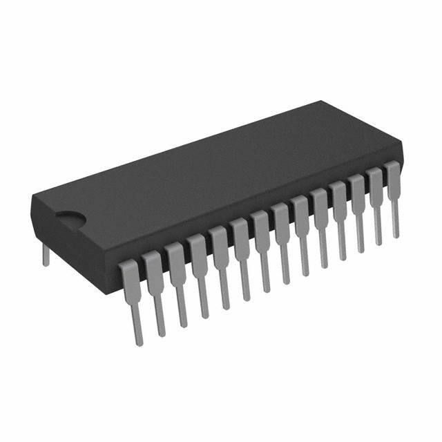
Figure 1. PDIP Package
See Package N0028E
www.ti.com
Figure 2. PLCC
Package
See Package FN0028A
These devices have limited built-in ESD protection. The leads should be shorted together or the device placed in conductive foam
during storage or handling to prevent electrostatic damage to the MOS gates.
Absolute Maximum Ratings (1) (2) (3)
Supply Voltage (VCC) (4)
6.5V
−0.3V to (VCC+0.3V)
Voltage at Any Pin Except Control Inputs
−0.3V to +15V
Voltage at Control Inputs
(START, OE, CLOCK, ALE, ADD A, ADD B, ADD C)
−65°C to +150°C
Storage Temperature Range
Package Dissipation at TA=25°C
875 mW
Lead Temp. (Soldering, 10 seconds)
PDIP Package (plastic)
PLCC Package
ESD Susceptibility
(1)
(2)
(3)
(4)
(5)
260°C
Vapor Phase (60 seconds)
215°C
Infrared (15 seconds)
220°C
(5)
400V
Absolute Maximum Ratings indicate limits beyond which damage to the device may occur. DC and AC electrical specifications do not
apply when operating the device beyond its specified operating conditions.
All voltages are measured with respect to GND, unless otherwise specified.
If Military/Aerospace specified devices are required, please contact the TI Sales Office/Distributors for availability and specifications.
A Zener diode exists, internally, from VCC to GND and has a typical breakdown voltage of 7 VDC.
Human body model, 100 pF discharged through a 1.5 kΩ resistor.
Operating Conditions
(1) (2)
TMIN≤TA≤TMAX
Temperature Range
−40°C≤TA≤+85°C
Range of VCC
(1)
(2)
4.5 VDC to 6.0 VDC
Absolute Maximum Ratings indicate limits beyond which damage to the device may occur. DC and AC electrical specifications do not
apply when operating the device beyond its specified operating conditions.
All voltages are measured with respect to GND, unless otherwise specified.
Electrical Characteristics – Converter Specifications
Converter Specifications: VCC=5 VDC=VREF+, VREF(−)=GND, TMIN≤TA≤TMAX and fCLK=640 kHz unless otherwise stated.
Symbol
Parameter
ADC0808
Total Unadjusted Error (1)
(1)
2
Conditions
Min
Typ
Max
Units
25°C
±½
LSB
TMIN to TMAX
±¾
LSB
Total unadjusted error includes offset, full-scale, linearity, and multiplexer errors. See Figure 5. None of these A/Ds requires a zero or
full-scale adjust. However, if an all zero code is desired for an analog input other than 0.0V, or if a narrow full-scale span exists (for
example: 0.5V to 4.5V full-scale) the reference voltages can be adjusted to achieve this. See Figure 15.
Submit Documentation Feedback
Copyright © 1999–2013, Texas Instruments Incorporated
Product Folder Links: ADC0808-N ADC0809-N
�ADC0808-N, ADC0809-N
www.ti.com
SNAS535H – OCTOBER 1999 – REVISED MARCH 2013
Electrical Characteristics – Converter Specifications (continued)
Converter Specifications: VCC=5 VDC=VREF+, VREF(−)=GND, TMIN≤TA≤TMAX and fCLK=640 kHz unless otherwise stated.
Symbol
Parameter
Conditions
ADC0809
Total Unadjusted Error (1)
VREF(+)
Max
Units
0°C to 70°C
±1
LSB
TMIN to TMAX
±1¼
LSB
VCC + 0.1
VDC
VCC
VCC + 0.1
V
(VCC/2) − 0.1
VCC/2
(VCC/2) + 0.1
V
−0.1
0
−2
±0.5
Input Resistance
From Ref(+) to Ref(−)
Analog Input Voltage Range
See
Voltage, Top of Ladder
Measured at Ref(+)
(2)
V(+) or V(−)
Voltage, Center of Ladder
VREF(−)
Voltage, Bottom of Ladder
IIN
fc=640 kHz,
Typ
1.0
2.5
GND − 0.1
Measured at Ref(−)
Comparator Input Current
(2)
Min
(3)
kΩ
V
μA
2
Two on-chip diodes are tied to each analog input which will forward conduct for analog input voltages one diode drop below ground or
one diode drop greater than the VCCn supply. The spec allows 100 mV forward bias of either diode. This means that as long as the
analog VIN does not exceed the supply voltage by more than 100 mV, the output code will be correct. To achieve an absolute 0VDC to
5VDC input voltage range will therefore require a minimum supply voltage of 4.900 VDC over temperature variations, initial tolerance and
loading.
Comparator input current is a bias current into or out of the chopper stabilized comparator. The bias current varies directly with clock
frequency and has little temperature dependence (Figure 8). See ANALOG COMPARATOR INPUTS
(3)
Electrical Characteristics – Digital Levels and DC Specifications
Digital Levels and DC Specifications: ADC0808CCN, ADC0808CCV, ADC0809CCN and ADC0809CCV, 4.75≤VCC≤5.25V,
−40°C≤TA≤+85°C unless otherwise noted
Symbol
Parameter
Conditions
Min
Typ
Max
Units
10
200
nA
1.0
μA
ANALOG MULTIPLEXER
VCC=5V, VIN=5V,
IOFF(+)
OFF Channel Leakage Current
TA=25°C
TMIN to TMAX
VCC=5V, VIN=0,
IOFF(−)
OFF Channel Leakage Current
TA=25°C
−200
−10
TMIN to TMAX
−1.0
μA
(VCC − 1.5)
V
nA
CONTROL INPUTS
VIN(1)
Logical “1” Input Voltage
VIN(0)
Logical “0” Input Voltage
IIN(1)
Logical “1” Input Current (The Control
Inputs)
VIN=15V
IIN(0)
Logical “0” Input Current (The Control
Inputs)
VIN=0
ICC
Supply Current
fCLK=640 kHz
1.5
V
1.0
μA
−1.0
μA
0.3
3.0
mA
DATA OUTPUTS AND EOC (INTERRUPT)
VOUT(1)
Logical “1” Output Voltage
VCC = 4.75V
IOUT = −360µA
IOUT = −10µA
VOUT(0)
Logical “0” Output Voltage
IO=1.6 mA
0.45
VOUT(0)
Logical “0” Output Voltage EOC
IO=1.2 mA
0.45
V
3
μA
IOUT
2.4
4.5
V
V
VO=5V
TRI-STATE Output Current
−3
VO=0
V
μA
Electrical Characteristics – Timing Specifications
Timing Specifications VCC=VREF(+)=5V, VREF(−)=GND, tr=tf=20 ns and TA=25°C unless otherwise noted.
Symbol
tSTCLK
Parameter
Conditions
Start Time Delay from Clock
(Figure 7)
Copyright © 1999–2013, Texas Instruments Incorporated
Product Folder Links: ADC0808-N ADC0809-N
MIn
300
Typ
Max
Units
900
ns
Submit Documentation Feedback
3
�ADC0808-N, ADC0809-N
SNAS535H – OCTOBER 1999 – REVISED MARCH 2013
www.ti.com
Electrical Characteristics – Timing Specifications (continued)
Timing Specifications VCC=VREF(+)=5V, VREF(−)=GND, tr=tf=20 ns and TA=25°C unless otherwise noted.
Symbol
Parameter
Conditions
MIn
Typ
Max
Units
tWS
Minimum Start Pulse Width
(Figure 7)
100
200
ns
tWALE
Minimum ALE Pulse Width
(Figure 7)
100
200
ns
ts
Minimum Address Set-Up Time
(Figure 7)
25
50
ns
tH
Minimum Address Hold Time
(Figure 7)
25
50
ns
tD
Analog MUX Delay Time From ALE
RS=0Ω (Figure 7)
1
2.5
μs
tH1, tH0
OE Control to Q Logic State
CL=50 pF, RL=10k (Figure 10)
125
250
ns
t1H, t0H
OE Control to Hi-Z
CL=10 pF, RL=10k (Figure 10)
125
250
ns
tc
Conversion Time
fc
Clock Frequency
tEOC
EOC Delay Time
(Figure 7)
CIN
Input Capacitance
At Control Inputs
COUT
TRI-STATE Output Capacitance
At TRI-STATE Outputs
(1)
4
fc=640 kHz, (Figure 7)
(1)
90
100
116
μs
10
640
1280
kHz
8 + 2 μS
Clock
Periods
10
15
pF
10
15
pF
0
The outputs of the data register are updated one clock cycle before the rising edge of EOC.
Submit Documentation Feedback
Copyright © 1999–2013, Texas Instruments Incorporated
Product Folder Links: ADC0808-N ADC0809-N
�ADC0808-N, ADC0809-N
www.ti.com
SNAS535H – OCTOBER 1999 – REVISED MARCH 2013
Functional Description
MULTIPLEXER
The device contains an 8-channel single-ended analog signal multiplexer. A particular input channel is selected
by using the address decoder. Table 1 shows the input states for the address lines to select any channel. The
address is latched into the decoder on the low-to-high transition of the address latch enable signal.
Table 1. Analog Channel Selection
ADDRESS LINE
SELECTED ANALOG
CHANNEL
C
B
IN0
L
L
L
IN1
L
L
H
IN2
L
H
L
IN3
L
H
H
IN4
H
L
L
IN5
H
L
H
IN6
H
H
L
IN7
H
H
H
A
CONVERTER CHARACTERISTICS
The Converter
The heart of this single chip data acquisition system is its 8-bit analog-to-digital converter. The converter is
designed to give fast, accurate, and repeatable conversions over a wide range of temperatures. The converter is
partitioned into 3 major sections: the 256R ladder network, the successive approximation register, and the
comparator. The converter's digital outputs are positive true.
The 256R ladder network approach (Figure 3) was chosen over the conventional R/2R ladder because of its
inherent monotonicity, which ensures no missing digital codes. Monotonicity is particularly important in closed
loop feedback control systems. A non-monotonic relationship can cause oscillations that will be catastrophic for
the system. Additionally, the 256R network does not cause load variations on the reference voltage.
The bottom resistor and the top resistor of the ladder network in Figure 3 are not the same value as the
remainder of the network. The difference in these resistors causes the output characteristic to be symmetrical
with the zero and full-scale points of the transfer curve. The first output transition occurs when the analog signal
has reached +½ LSB and succeeding output transitions occur every 1 LSB later up to full-scale.
The successive approximation register (SAR) performs 8 iterations to approximate the input voltage. For any
SAR type converter, n-iterations are required for an n-bit converter. Figure 4 shows a typical example of a 3-bit
converter. In the ADC0808, ADC0809, the approximation technique is extended to 8 bits using the 256R
network.
The A/D converter's successive approximation register (SAR) is reset on the positive edge of the start conversion
start pulse. The conversion is begun on the falling edge of the start conversion pulse. A conversion in process
will be interrupted by receipt of a new start conversion pulse. Continuous conversion may be accomplished by
tying the end-of-conversion (EOC) output to the SC input. If used in this mode, an external start conversion pulse
should be applied after power up. End-of-conversion will go low between 0 and 8 clock pulses after the rising
edge of start conversion.
The most important section of the A/D converter is the comparator. It is this section which is responsible for the
ultimate accuracy of the entire converter. It is also the comparator drift which has the greatest influence on the
repeatability of the device. A chopper-stabilized comparator provides the most effective method of satisfying all
the converter requirements.
The chopper-stabilized comparator converts the DC input signal into an AC signal. This signal is then fed through
a high gain AC amplifier and has the DC level restored. This technique limits the drift component of the amplifier
since the drift is a DC component which is not passed by the AC amplifier. This makes the entire A/D converter
extremely insensitive to temperature, long term drift and input offset errors.
Copyright © 1999–2013, Texas Instruments Incorporated
Product Folder Links: ADC0808-N ADC0809-N
Submit Documentation Feedback
5
�ADC0808-N, ADC0809-N
SNAS535H – OCTOBER 1999 – REVISED MARCH 2013
www.ti.com
Figure 6 shows a typical error curve for the ADC0808.
Figure 3. Resistor Ladder and Switch Tree
Figure 4. 3-Bit A/D Transfer Curve
Figure 5. 3-Bit A/D Absolute Accuracy Curve
Figure 6. Typical Error Curve
6
Submit Documentation Feedback
Copyright © 1999–2013, Texas Instruments Incorporated
Product Folder Links: ADC0808-N ADC0809-N
�ADC0808-N, ADC0809-N
www.ti.com
SNAS535H – OCTOBER 1999 – REVISED MARCH 2013
Timing Diagram
Figure 7.
Copyright © 1999–2013, Texas Instruments Incorporated
Product Folder Links: ADC0808-N ADC0809-N
Submit Documentation Feedback
7
�ADC0808-N, ADC0809-N
SNAS535H – OCTOBER 1999 – REVISED MARCH 2013
www.ti.com
Typical Performance Characteristics
Comparator IIN
vs
VIN
(VCC=VREF=5V)
Figure 8.
Multiplexer RON
vs
VIN
(VCC=VREF=5V)
Figure 9.
8
Submit Documentation Feedback
Copyright © 1999–2013, Texas Instruments Incorporated
Product Folder Links: ADC0808-N ADC0809-N
�ADC0808-N, ADC0809-N
www.ti.com
SNAS535H – OCTOBER 1999 – REVISED MARCH 2013
TRI-STATE Test Circuits and Timing Diagrams
t1H, tH1
t0H, tH0
t1H, CL = 10 pF
t0H, CL = 10 pF
tH1, CL = 50 pF
tH0, CL = 50 pF
tr
tr
90%
50%
10%
90%
50%
10%
tH1
tH0
50%
50%
Figure 10. TRI-STATE Test Circuits and Timing Diagrams
Copyright © 1999–2013, Texas Instruments Incorporated
Product Folder Links: ADC0808-N ADC0809-N
Submit Documentation Feedback
9
�ADC0808-N, ADC0809-N
SNAS535H – OCTOBER 1999 – REVISED MARCH 2013
www.ti.com
APPLICATIONS INFORMATION
OPERATION
RATIOMETRIC CONVERSION
The ADC0808, ADC0809 is designed as a complete Data Acquisition System (DAS) for ratiometric conversion
systems. In ratiometric systems, the physical variable being measured is expressed as a percentage of full-scale
which is not necessarily related to an absolute standard. The voltage input to the ADC0808 is expressed by the
equation
•
•
•
•
•
•
VIN= Input voltage into the ADC0808
Vfs= Full-scale voltage
VZ= Zero voltage
DX= Data point being measured
DMAX= Maximum data limit
DMIN= Minimum data limit
(1)
A good example of a ratiometric transducer is a potentiometer used as a position sensor. The position of the
wiper is directly proportional to the output voltage which is a ratio of the full-scale voltage across it. Since the
data is represented as a proportion of full-scale, reference requirements are greatly reduced, eliminating a large
source of error and cost for many applications. A major advantage of the ADC0808, ADC0809 is that the input
voltage range is equal to the supply range so the transducers can be connected directly across the supply and
their outputs connected directly into the multiplexer inputs, (Figure 11).
Ratiometric transducers such as potentiometers, strain gauges, thermistor bridges, pressure transducers, etc.,
are suitable for measuring proportional relationships; however, many types of measurements must be referred to
an absolute standard such as voltage or current. This means a system reference must be used which relates the
full-scale voltage to the standard volt. For example, if VCC=VREF=5.12V, then the full-scale range is divided into
256 standard steps. The smallest standard step is 1 LSB which is then 20 mV.
RESISTOR LADDER LIMITATIONS
The voltages from the resistor ladder are compared to the selected into 8 times in a conversion. These voltages
are coupled to the comparator via an analog switch tree which is referenced to the supply. The voltages at the
top, center and bottom of the ladder must be controlled to maintain proper operation.
The top of the ladder, Ref(+), should not be more positive than the supply, and the bottom of the ladder, Ref(−),
should not be more negative than ground. The center of the ladder voltage must also be near the center of the
supply because the analog switch tree changes from N-channel switches to P-channel switches. These
limitations are automatically satisfied in ratiometric systems and can be easily met in ground referenced systems.
Figure 12 shows a ground referenced system with a separate supply and reference. In this system, the supply
must be trimmed to match the reference voltage. For instance, if a 5.12V is used, the supply should be adjusted
to the same voltage within 0.1V.
Figure 11. Ratiometric Conversion System
10
Submit Documentation Feedback
Copyright © 1999–2013, Texas Instruments Incorporated
Product Folder Links: ADC0808-N ADC0809-N
�ADC0808-N, ADC0809-N
www.ti.com
SNAS535H – OCTOBER 1999 – REVISED MARCH 2013
The ADC0808 needs less than a milliamp of supply current so developing the supply from the reference is
readily accomplished. In Figure 13 a ground referenced system is shown which generates the supply from the
reference. The buffer shown can be an op amp of sufficient drive to supply the milliamp of supply current and the
desired bus drive, or if a capacitive bus is driven by the outputs a large capacitor will supply the transient supply
current as seen in Figure 14. The LM301 is overcompensated to insure stability when loaded by the 10 μF output
capacitor.
The top and bottom ladder voltages cannot exceed VCC and ground, respectively, but they can be symmetrically
less than VCC and greater than ground. The center of the ladder voltage should always be near the center of the
supply. The sensitivity of the converter can be increased, (i.e., size of the LSB steps decreased) by using a
symmetrical reference system. In Figure 15, a 2.5V reference is symmetrically centered about VCC/2 since the
same current flows in identical resistors. This system with a 2.5V reference allows the LSB bit to be half the size
of a 5V reference system.
Figure 12. Ground Referenced
Conversion System Using Trimmed Supply
Figure 13. Ground Referenced Conversion System with
Reference Generating VCC Supply
Copyright © 1999–2013, Texas Instruments Incorporated
Product Folder Links: ADC0808-N ADC0809-N
Submit Documentation Feedback
11
�ADC0808-N, ADC0809-N
SNAS535H – OCTOBER 1999 – REVISED MARCH 2013
www.ti.com
Figure 14. Typical Reference and Supply Circuit
RA=RB
*Ratiometric transducers
Figure 15. Symmetrically Centered Reference
CONVERTER EQUATIONS
The transition between adjacent codes N and N+1 is given by:
(2)
The center of an output code N is given by:
(3)
The output code N for an arbitrary input are the integers within the range:
Where:
•
•
•
•
•
12
VIN=Voltage at comparator input
VREF(+)=Voltage at Ref(+)
VREF(−)=Voltage at Ref(−)
VTUE=Total unadjusted error voltage (typically
VREF(+)÷512)
Submit Documentation Feedback
(4)
Copyright © 1999–2013, Texas Instruments Incorporated
Product Folder Links: ADC0808-N ADC0809-N
�ADC0808-N, ADC0809-N
www.ti.com
SNAS535H – OCTOBER 1999 – REVISED MARCH 2013
ANALOG COMPARATOR INPUTS
The dynamic comparator input current is caused by the periodic switching of on-chip stray capacitances. These
are connected alternately to the output of the resistor ladder/switch tree network and to the comparator input as
part of the operation of the chopper stabilized comparator.
The average value of the comparator input current varies directly with clock frequency and with VIN as shown in
Figure 8.
If no filter capacitors are used at the analog inputs and the signal source impedances are low, the comparator
input current should not introduce converter errors, as the transient created by the capacitance discharge will die
out before the comparator output is strobed.
If input filter capacitors are desired for noise reduction and signal conditioning they will tend to average out the
dynamic comparator input current. It will then take on the characteristics of a DC bias current whose effect can
be predicted conventionally.
Typical Application
*Address latches needed for 8085 and SC/MP interfacing the ADC0808 to a microprocessor
Table 2. Microprocessor Interface Table
PROCESSOR
READ
WRITE
INTERRUPT (COMMENT)
8080
MEMR
MEMW
INTR (Thru RST Circuit)
8085
RD
WR
INTR (Thru RST Circuit)
Z-80
RD
WR
INT (Thru RST Circuit, Mode 0)
SC/MP
NRDS
NWDS
SA (Thru Sense A)
6800
VMA•φ2•R/W
VMA•φ•R/W
IRQA or IRQB (Thru PIA)
Copyright © 1999–2013, Texas Instruments Incorporated
Product Folder Links: ADC0808-N ADC0809-N
Submit Documentation Feedback
13
�ADC0808-N, ADC0809-N
SNAS535H – OCTOBER 1999 – REVISED MARCH 2013
www.ti.com
REVISION HISTORY
Changes from Revision G (March 2013) to Revision H
•
14
Page
Changed layout of National Data Sheet to TI format .......................................................................................................... 13
Submit Documentation Feedback
Copyright © 1999–2013, Texas Instruments Incorporated
Product Folder Links: ADC0808-N ADC0809-N
�PACKAGE OPTION ADDENDUM
www.ti.com
10-Dec-2020
PACKAGING INFORMATION
Orderable Device
Status
(1)
Package Type Package Pins Package
Drawing
Qty
Eco Plan
(2)
Lead finish/
Ball material
MSL Peak Temp
Op Temp (°C)
Device Marking
(3)
(4/5)
(6)
ADC0808CCV/NOPB
ACTIVE
PLCC
FN
28
35
RoHS & Green
SN
Level-2A-245C-4
WEEK
-40 to 85
ADC0808
CCV
ADC0808CCVX/NOPB
ACTIVE
PLCC
FN
28
750
RoHS & Green
SN
Level-2A-245C-4
WEEK
-40 to 85
ADC0808
CCV
ADC0809CCV/NOPB
ACTIVE
PLCC
FN
28
35
RoHS & Green
SN
Level-2A-245C-4
WEEK
-40 to 85
ADC0809
CCV
ADC0809CCVX/NOPB
ACTIVE
PLCC
FN
28
750
RoHS & Green
SN
Level-2A-245C-4
WEEK
-40 to 85
ADC0809
CCV
(1)
The marketing status values are defined as follows:
ACTIVE: Product device recommended for new designs.
LIFEBUY: TI has announced that the device will be discontinued, and a lifetime-buy period is in effect.
NRND: Not recommended for new designs. Device is in production to support existing customers, but TI does not recommend using this part in a new design.
PREVIEW: Device has been announced but is not in production. Samples may or may not be available.
OBSOLETE: TI has discontinued the production of the device.
(2)
RoHS: TI defines "RoHS" to mean semiconductor products that are compliant with the current EU RoHS requirements for all 10 RoHS substances, including the requirement that RoHS substance
do not exceed 0.1% by weight in homogeneous materials. Where designed to be soldered at high temperatures, "RoHS" products are suitable for use in specified lead-free processes. TI may
reference these types of products as "Pb-Free".
RoHS Exempt: TI defines "RoHS Exempt" to mean products that contain lead but are compliant with EU RoHS pursuant to a specific EU RoHS exemption.
Green: TI defines "Green" to mean the content of Chlorine (Cl) and Bromine (Br) based flame retardants meet JS709B low halogen requirements of