ADC08351
www.ti.com
SNAS026E – JUNE 2000 – REVISED MARCH 2013
ADC08351 8-Bit, 42 MSPS, 40 mW A/D Converter
Check for Samples: ADC08351
FEATURES
DESCRIPTION
•
•
•
•
•
The ADC08351 is an easy to use low power, low
cost, small size, 42 MSPS analog-to-digital converter
that digitizes signals to 8 bits. The ADC08351 uses
an unique architecture that achieves 7.2 Effective Bits
with a 4.4 MHz input and 42 MHz clock frequency
and 6.8 Effective Bits with a 21 MHz input and 42
MHz clock frequency. Output formatting is straight
binary coding.
1
2
Low Input Capacitance
Internal Sample-and-Hold Function
Single +3V Operation
Power Down Feature
TRI-STATE Outputs
KEY SPECIFICATIONS
•
•
•
•
•
Resolution: 8 Bits
Maximum Sampling Frequency: 42MSPS (min)
ENOB @ fCLK = 42 MHz,
fIN = 4.4 MHz: 7.2 Bits (typ)
Ensured No Missing Codes
Power Consumption: 40 mW (typ); 48 mW
(max) (Excluding Reference Current)
APPLICATIONS
•
•
•
•
•
•
•
•
•
Video Digitization
Digital Still Cameras
Set Top Boxes
Digital Camcorders
Communications
Medical Imaging
Personal Computer Video
CCD Imaging
Electro-Optics
To minimize system cost and power consumption, the
ADC08351 requires minimal external components
and includes input biasing to allow optional a.c. input
signal coupling. The user need only provide a +3V
supply and a clock. Many applications require no
separate reference or driver components.
The excellent dc and ac characteristics of this device,
together with its low power consumption and +3V
single supply operation, make it ideally suited for
many video and imaging applications, including use in
portable equipment. Total power consumption is
reduced to less than 7 mW in the power-down mode.
Furthermore, the ADC08351 is resistant to latch-up
and the outputs are short-circuit proof.
Fabricated on a 0.35 micron CMOS process, the
ADC08351 is offered in TSSOP and WQFN (a
molded lead frame-based chip-scale package), and is
designed to operate over the industrial temperature
range of −40°C to +85°C.
1
2
Please be aware that an important notice concerning availability, standard warranty, and use in critical applications of
Texas Instruments semiconductor products and disclaimers thereto appears at the end of this data sheet.
All trademarks are the property of their respective owners.
PRODUCTION DATA information is current as of publication date.
Products conform to specifications per the terms of the Texas
Instruments standard warranty. Production processing does not
necessarily include testing of all parameters.
Copyright © 2000–2013, Texas Instruments Incorporated
�ADC08351
SNAS026E – JUNE 2000 – REVISED MARCH 2013
www.ti.com
ADC08351 Block Diagram
Pin Configuration
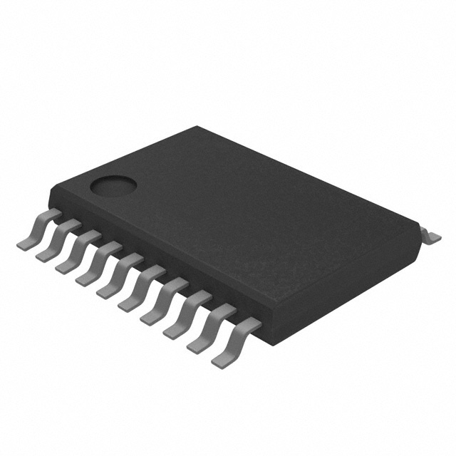
Figure 1. 20-Pin TSSOP - Top View
2
Figure 2. 24-Pin WQFN (CSP) - Bottom View
Submit Documentation Feedback
Copyright © 2000–2013, Texas Instruments Incorporated
Product Folder Links: ADC08351
�ADC08351
www.ti.com
SNAS026E – JUNE 2000 – REVISED MARCH 2013
PIN DESCRIPTIONS AND EQUIVALENT CIRCUITS (1)
Pin
No.
Symbol
17
(17)
VIN
Analog signal input. Conversion range is 0.5 VP-P to 0.68 VA.
14
(14)
VREF
Positive reference voltage input. Operating range of this
voltage is 0.75V to VA. This pin should be bypassed with a 10
µF tantalum or aluminum electrolytic capacitor and a 0.1 µF
ceramic chip capacitor.
1
(22)
OE
CMOS/TTL compatible digital input that, when low, enables
the digital outputs of the ADC08351. When high, the outputs
are in a high impedance state.
12
(11)
CLK
CMOS/TTL compatible digital clock input. VIN is sampled on
the falling edge of CLK input.
Equivalent Circuit
Description
CMOS/TTL compatible digital input that, when high, puts the
ADC08351 into the power down mode, where it consumes
minimal power. When this pin is low, the ADC08351 is in the
normal operating mode.
15
(15)
PD
3 thru
10
(1 thru
8)
D0–D7
Conversion data digital output pins. D0 is the LSB, D7 is the
MSB. Valid data is output just after the rising edge of the CLK
input. These pins are enabled by bringing the OE pin low.
11, 13
(10, 12)
VD
Positive digital supply pin. Connect to a clean, quiet voltage
source of +3V. VA and VD should have a common supply and
be separately bypassed with a 10 µF tantalum or aluminum
electrolytic capacitor and a 0.1 µF ceramic chip capacitor.
See Layout and Grounding for more information.
2, 20
(21, 23)
DGND
The ground return for the digital supply. AGND and DGND
should be connected together close to the ADC08351.
16
(16)
VA
Positive analog supply pin. Connected to a clean, quiet
voltage source of +3V. VA and VD should have a common
supply and be separately bypassed with a 10 µF tantalum or
aluminum electrolytic capacitor and a 0.1 µF ceramic chip
capacitor. See Layout and Grounding for more information.
18, 19
(18, 19)
AGND
The ground return for the analog supply. AGND and DGND
should be connected together close to the ADC08351
package.
(1)
WQFN pins in parentheses
These devices have limited built-in ESD protection. The leads should be shorted together or the device placed in conductive foam
during storage or handling to prevent electrostatic damage to the MOS gates.
Submit Documentation Feedback
Copyright © 2000–2013, Texas Instruments Incorporated
Product Folder Links: ADC08351
3
�ADC08351
SNAS026E – JUNE 2000 – REVISED MARCH 2013
www.ti.com
Absolute Maximum Ratings (1) (2) (3)
Supply Voltage (VA, VD)
4.2V
−0.3V to 4.2V
Voltage on Any Input or Output Pin
Ground Difference (AGND–DGND)
±100 mV
−0.5 to (VA + 0.5V)
CLK, OE Voltage Range
Digital Output Voltage (VOH, VOL)
VD to DGND
Input Current at Any Pin (4)
±25 mA
Package Input Current (4)
±50 mA
See (5)
Package Dissipation at TA = 25°C
ESD Susceptibility
(6)
Human Body Model
Machine Model
Soldering Temp., Infrared, 10 sec.
(7)
(3)
(4)
(5)
(6)
(7)
200V
235°C
−65°C to +150°C
Storage Temperature
(1)
(2)
4000V
All voltages are measured with respect to GND = AGND = DGND = 0V, unless otherwise specified.
Absolute Maximum Ratings indicate limits beyond which damage to the device may occur. Operating Ratings indicate conditions for
which the device is functional, but do not ensure specific performance limits. For ensured specifications and test conditions, see the
Electrical Characteristics. The ensured specifications apply only for the test conditions listed. Some performance characteristics may
degrade when the device is not operated under the listed test conditions.
If Military/Aerospace specified devices are required, please contact the TI Sales Office/ Distributors for availability and specifications.
When the input voltage at any pin exceeds the power supplies (that is, less than AGND or DGND, or greater than VA or VD), the current
at that pin should be limited to 25 mA. The 50 mA maximum package input current rating limits the number of pins that can safely
exceed the power supplies with an input current of 25 mA to two.
The absolute maximum junction temperature (TJmax) for this device is 150°C. The maximum allowable power dissipation is dictated by
TJmax, the junction-to-ambient thermal resistance (θJA), and the ambient temperature (TA), and can be calculated using the formula
PDMAX = (TJmax - TA)/θJA. For the 20-pin TSSOP, θJA is 135°C/W, so PDMAX = 926 mW at 25°C and 481 mW at the maximum
operating ambient temperature of 85°C. Note that the power dissipation of this device under normal operation will typically be about 68
mW (40 mW quiescent power + 23 mW reference ladder power + 5 mW due to 1 TTL loan on each digital output). The values for
maximum power dissipation listed above will be reached only when the ADC08351 is operated in a severe fault condition (e.g., when
input or output pins are driven beyond the power supply voltages, or the power supply polarity is reversed). Obviously, such conditions
should always be avoided.
Human body model is 100 pF capacitor discharged through a 1.5 kΩ resistor. Machine model is 220 pF discharged through ZERO
Ohms.
See AN-450, “Surface Mounting Methods and Their Effect on Product Reliability”, or the section entitled “Surface Mount” found in any
post 1986 Texas Instruments Linear Data Book, for other methods of soldering surface mount devices.
Operating Ratings (1) (2)
−40°C TA ≤ +85°C
Operating Temperature Range
Supply Voltage (VA, VD)
+2.7V to +3.6V
Ground Difference |DGND–AGND|
0V to 100 mV
VIN Voltage Range (VP-P)
(1)
(2)
4
0.5V to 0.68 VA
Absolute Maximum Ratings indicate limits beyond which damage to the device may occur. Operating Ratings indicate conditions for
which the device is functional, but do not ensure specific performance limits. For ensured specifications and test conditions, see the
Electrical Characteristics. The ensured specifications apply only for the test conditions listed. Some performance characteristics may
degrade when the device is not operated under the listed test conditions.
All voltages are measured with respect to GND = AGND = DGND = 0V, unless otherwise specified.
Submit Documentation Feedback
Copyright © 2000–2013, Texas Instruments Incorporated
Product Folder Links: ADC08351
�ADC08351
www.ti.com
SNAS026E – JUNE 2000 – REVISED MARCH 2013
Converter Electrical Characteristics
The following specifications apply for VA = VD = +3.0 VDC, VREF = 2.4V, VIN = 1.63 VP-P, OE = 0V, CL = 20 pF, fCLK = 42 MHz,
50% duty cycle, unless otherwise specified.
Boldface limits apply for TA = TMIN to TMAX: all other limits TA = 25°C (1) (2)
Symbol
Parameter
Typical (3)
Conditions
Limits (3)
Units
(Limits)
DC Accuracy
INL
Integral Non Linearity Error
DNL
Differential Non Linearity
±0.7
±0.6
Missing Codes
±1.4
LSB (max)
+1.3
LSB (max)
−1.0
LSB (min)
0
(max)
EZ
Zero Scale Offset Error
−17
mV
EFS
Full Scale Offset Error
−7
mV
Video Accuracy
DP
Differential Phase Error
fCLK = 20 MHz, Video Ramp Input
1.0
Degree
DG
Differential Gain Error
fCLK = 20 MHz, Video Ramp Input
1.5
%
(CLK LOW)
4
pF
(CLK HIGH)
11
pF
Analog Input and Reference Characteristics
CIN
VIN Input Capacitance
VIN = 1.5V + 0.7 Vrms
RIN
RIN Input Resistance
7.2
kΩ
FPBW
Full-Power Bandwidth
120
MHz
VREF
Reference Input Voltage
0.735
V
IREF
Reference Input Current
At pin 14
VA
V
7.7
mA
PD = Low
10.5
mA
PD = High
1
mA
PD = Low, No Digital Output Load
2.9
mA
PD = High
0.5
Total Operating Current
Excluding Reference Current, VIN = 0 VDC
13.4
16
mA (max)
Power Consumption (active)
PD = Low (excluding reference current)
40.2
48
mW (max)
Power Consumption (power down)
PD = High (excluding reference current)