OBSOLETE
ADC1005
www.ti.com
SNAS526F – JUNE 1999 – REVISED APRIL 2013
ADC1005 10-Bit μP Compatible A/D Converter
Check for Samples: ADC1005
FEATURES
DESCRIPTION
•
•
•
NOTE: This device is obsolete. This data sheet is
provided for information only.
1
23
•
•
•
•
Easy interface to all microprocessors
Differential analog voltage inputs
Operates ratiometrically or with 5 VDC voltage
reference or analog span adjusted voltage
reference
0V to 5V analog input voltage range with
single 5V supply
On-chip clock generator
TLL/MOS input/output compatible
0.3″ standard width 20-pin DIP
KEY SPECIFICATIONS
•
•
•
The ADC1005 is a CMOS 10-bit successive
approximation A/D converter. The 20-pin ADC1005
outputs 10-bit data in a two-byte format for interface
with 8-bit microprocessors.
The ADC1005 has differential inputs to permit
rejection of common-mode signals, allow the analog
input range to be offset, and also to permit the
conversion of signals not referred to ground. In
addition, the reference voltage can be adjusted,
allowing smaller voltage spans to be measured with
10-bit resolution.
Resolution 10 bits
Linearity Error ±½ LSB and ±1 LSB
Conversion Time 50 μs
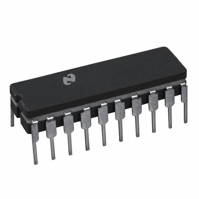
Connection Diagram
Figure 1. ADC 1005 (for an 8–bit data bus)
Dual-In-Line Package - Top View
These devices have limited built-in ESD protection. The leads should be shorted together or the device placed in conductive foam
during storage or handling to prevent electrostatic damage to the MOS gates.
1
2
3
Please be aware that an important notice concerning availability, standard warranty, and use in critical applications of
Texas Instruments semiconductor products and disclaimers thereto appears at the end of this data sheet.
TRI-STATE is a registered trademark of Texas Instruments.
All other trademarks are the property of their respective owners.
PRODUCTION DATA information is current as of publication date.
Products conform to specifications per the terms of the Texas
Instruments standard warranty. Production processing does not
necessarily include testing of all parameters.
Copyright © 1999–2013, Texas Instruments Incorporated
�OBSOLETE
ADC1005
SNAS526F – JUNE 1999 – REVISED APRIL 2013
www.ti.com
Absolute Maximum Ratings (1) (2) (3)
Supply Voltage (VCC)
6.5V
−0.3V to +15V
Logic Control Inputs
−0.3V to VCC +0.3V
Voltage at Other Inputs and Outputs
Input Current Per Pin
±5 mA
Input Current Per Package
±20 mA
−65°C to +150°C
Storage Temperature Range
Package Dissipation at TA=25°C
875 mW
Lead Temperature
Soldering, 10 seconds
Dual-In-Line Package (Ceramic)
300°C
ESD Susceptibility (4)
(1)
(2)
(3)
(4)
800V
All voltages are measured with respect to ground.
Absolute Maximum Ratings indicate limits beyond which damage to the device may occur. DC and AC electrical specifications do not
apply when operating the device beyond its specified operating conditions.
If Military/Aerospace specified devices are required, please contact the Texas Instruments Sales Office/ Distributors for availability and
specifications.
Human body model, 100 pF discharged through a 1.5 kΩ resistor.
Operating Ratings (1) (2)
Supply Voltage (VCC)
4.5V to 6.0V
TMN≤TA≤TMAX
Temperature Range
ADC1005BCJ
(1)
(2)
−40°C≤TA≤+85°C
ADC1005BCJ-1, ADC1005CCJ-1
Absolute Maximum Ratings indicate limits beyond which damage to the device may occur. DC and AC electrical specifications do not
apply when operating the device beyond its specified operating conditions.
All voltages are measured with respect to ground.
Electrical Characteristics
The following specifications apply for VCC = 5V, VREF = 5V, fCLK = 1.8 MHz unless otherwise specified. Boldface limits apply
from TMIN to TMAX; All other limits TA = Tj = 25°C.
ADC1005BCJ
Parameter
ADC1005BCJ-1,
ADC1005CCJ-1
Conditions
Typ
(1)
Tested
Limit (2)
Design
Limit (3)
Typ
(1)
Limit
Units
Tested
Limit (2)
Design
Limit (3)
ADC1005BCJ-1
±0.5
±0.5
LSB
ADC1005CCJ-1
±1
±1
LSB
ADC1005BCJ-1
±0.5
±0.5
LSB
ADC1005CCJ-1
±1
±1
LSB
Converter Characteristics
Linearity Error (4)
ADC1005BCJ
±0.5
LSB
Zero Error
ADC1005BCJ
±0.5
LSB
Fullscale Error
ADC1005BCJ
±0.5
LSB
ADC1005BCJ-1
±0.5
±0.5
LSB
ADC1005CCJ-1
±1
±1
LSB
Reference
MIN
4.8
2.2
4.8
2.4
2.2
kΩ
Input
MAX
4.8
8.3
4.8
7.6
8.3
kΩ
Resistance
(1)
(2)
(3)
(4)
2
Typicals are at 25°C and represent most likely parametric norm.
Tested and guaranteed to TI's AOQL (Average Outgoing Quality Level).
Guaranteed, but not 100% production tested. These limits are not used to calculate outgoing quality levels.
Linearity error is defined as the deviation of the analog value, expressed in LSBs, from the straight line which passes through the end
points of the transfer characteristic.
Submit Documentation Feedback
Copyright © 1999–2013, Texas Instruments Incorporated
Product Folder Links: ADC1005
�OBSOLETE
ADC1005
www.ti.com
SNAS526F – JUNE 1999 – REVISED APRIL 2013
Electrical Characteristics (continued)
The following specifications apply for VCC = 5V, VREF = 5V, fCLK = 1.8 MHz unless otherwise specified. Boldface limits apply
from TMIN to TMAX; All other limits TA = Tj = 25°C.
ADC1005BCJ
Parameter
ADC1005CCJ-1
Conditions
Typ
Common-Mode
MIN
Input (5)
MAX
DC Common-Mode Error
(1)
VIN(+) or VIN(−)
Over CommonMode
ADC1005BCJ-1,
Tested
Limit (2)
Design
Limit (3)
Typ
(1)
Tested
Limit (2)
Design
Limit (3)
Limit
Units
VCC+0.05
VCC+0.05
VCC+0.05
V
GND−0.05
GND−0.05
GND−0.05
V
±⅛
±¼
±⅛
±¼
±¼
LSB
±⅛
±¼
±⅛
±¼
±¼
LSB
2.0
2.0
2.0
V
0.8
0.8
0.8
V
Input Range
Power Supply Sensitivity
VCC=5 VDC±5%
VREF = 4.75V
DC Characteristics
VIN(1) Logical “1” Input
Voltage
VCC=5.25V
MIN
VIN(0), Logical “0” Input
Voltage
VCC=4.75V
MAX (Except CLKIN )
IIN, Logical “1” Input
Current
VIN=5.0V
0.005
1
0.005
1
1
μA
VIN=0V
−0.005
−1
−0.005
−1
−1
μA
3.1
2.7
3.1
2.7
2.7
V
3.1
3.5
3.1
3.5
3.5
V
1.8
1.5
1.8
1.5
1.5
V
1.8
2.1
1.8
2.1
2.1
V
1.3
0.6
1.3
0.6
0.6
V
1.3
2.0
1.3
2.0
2.0
V
MAX
IIN, Logical “0” Input
Current
(except CLKIN )
MAX
VT+(MIN), Minimum CLKIN
Positive going Threshold
Voltage
VT(MAX), Maximum CLKIN
Positive going Threshold
Voltage
VT−(MIN), Minimum CLKIN
Negative going Threshold
Voltage
VT−(MAX), Maximum CLKIN
Negative going Threshold
Voltage
VH(MIN), Minimum CLKIN
Hysteresis (VT+-VT−)
VH(MAX), Maximum CLKIN
Hysteresis (VT+-VT−)
VOUT(1), Logical “1”
Output Voltage
VCC=4.75V
MIN
VOUT(0), Logical “0”
Output Voltage
2.4
2.8
2.4
V
IOUT=−10 μA
4.5
4.6
4.5
V
VCC=4.75V
0.4
0.34
0.4
V
−0.3
−3
μA
MAX IOUT=1.6 mA
IOUT, TRI-STATE® Output
(5)
IOUT=−360 μA
VOUT = 0V
−0.01
−3
−0.01
For VIN(−)≥VIN(+) the digital output code will be 00 0000 0000. Two on-chip diodes are tied to each analog input which will forward
conduct for analog input voltages one diode drop below ground or one diode drop greater than VCC supply. Be careful, during testing at
low VCC levels (4.5V), as high level analog inputs (5V) can cause this input diode to conduct, especially at elevated temperatures, and
cause errors for analog inputs near full-scale. The spec allows 50 mV forward bias of either diode. This means that as long as the
analog VIN does not exceed the supply voltage by more than 50 mV, the output code will be correct. To achieve an absolute 0 VDC to 5
VDC input voltage range will therefore require a minimum supply voltage of 4.950 VDC over temperature variations, initial tolerance and
loading.
Submit Documentation Feedback
Copyright © 1999–2013, Texas Instruments Incorporated
Product Folder Links: ADC1005
3
�OBSOLETE
ADC1005
SNAS526F – JUNE 1999 – REVISED APRIL 2013
www.ti.com
Electrical Characteristics (continued)
The following specifications apply for VCC = 5V, VREF = 5V, fCLK = 1.8 MHz unless otherwise specified. Boldface limits apply
from TMIN to TMAX; All other limits TA = Tj = 25°C.
ADC1005BCJ
Parameter
ADC1005CCJ-1
Conditions
Typ
Current
Current
(1)
Tested
Limit (2)
Design
Limit (3)
Typ
(1)
Tested
Limit (2)
Design
Limit (3)
Limit
Units
0.01
3
0.01
0.3
3
μA
VOUT=0V
−14
−6.5
−14
−7.5
−6.5
mA
VOUT=5V
16
8.0
16
9.0
8.0
mA
1.5
3
1.5
2.5
3
mA
MAX VOUT = 5V
ISOURCE, Output Source
ADC1005BCJ-1,
MIN
ISINK, Output Sink
Current
MIN
ICC, Supply Current
MAX fCLK=1.8 MHz
CS =“1”
AC Electrical Characteristics
The following specifications apply for VCC = 5V, VREF = 5V,VREF = 5V, tr= tf= 20 ns unless otherwise specified. Boldface limits
apply from TMIN to TMAX; All other limits TA = Tj = 25°C.
Tested
Limit (2)
Design
Limit (3)
Limit
Units
MIN
0.2
0.2
MHz
MAX
2.6
2.6
MHz
MIN
40
40
%
MAX
60
60
%
MIN
80
80
1/fCLK
MAX
90
90
1/fCLK
Parameter
fCLK, Clock Frequency
Clock Duty Cycle
tC, Conversion Time
Conditions
Typ (1)
MIN
fCLK=1.8 MHz
45
45
μs
MAX
fCLK=1.8 MHz
50
50
μs
tW(WR)L, Minimum WR Pulse
Width
CS =0
100
150
150
ns
tACC, Access Time (Delay from
falling edge of RD to Output Data
Valid)
CS =0
170
300
300
ns
t1H, t0H, TRI-STATE Control
(Delay from Rising Edge of RD to
Hi-Z State)
RL=10k, CL=10 pF
125
200
ns
RL=2k, CL=100 pF
145
230
230
ns
300
450
450
ns
400
550
550
ns
CL=100 pF, RL = 2k
tWI, tRI, Delay from Falling Edge of
WR or RD to Reset of INTR
tIRS, INTR to 1st Read Set-up
Time
CIN, Capacitance of Logic Inputs
5
7.5
pF
COUT, Capacitance of Logic
Outputs
5
7.5
pF
(1)
(2)
(3)
4
Typicals are at 25°C and represent most likely parametric norm.
Tested and guaranteed to TI's AOQL (Average Outgoing Quality Level).
Guaranteed, but not 100% production tested. These limits are not used to calculate outgoing quality levels.
Submit Documentation Feedback
Copyright © 1999–2013, Texas Instruments Incorporated
Product Folder Links: ADC1005
�OBSOLETE
ADC1005
www.ti.com
SNAS526F – JUNE 1999 – REVISED APRIL 2013
Functional Diagram
Submit Documentation Feedback
Copyright © 1999–2013, Texas Instruments Incorporated
Product Folder Links: ADC1005
5
�OBSOLETE
ADC1005
SNAS526F – JUNE 1999 – REVISED APRIL 2013
www.ti.com
Typical Performance Characteristics
Logic Input Threshold
Voltage
vs
Supply Voltage
Delay from Falling Edge of
RD to Output data Valid vs
Load Capacitance
Figure 2.
Figure 3.
CLK IN Schmitt Trip Levels
vs Supply Voltage
Output Current vs
Temperature
Figure 4.
Figure 5.
Typical Linearity Error
vs Clock Frequency
Figure 6.
6
Submit Documentation Feedback
Copyright © 1999–2013, Texas Instruments Incorporated
Product Folder Links: ADC1005
�OBSOLETE
ADC1005
www.ti.com
SNAS526F – JUNE 1999 – REVISED APRIL 2013
TEST CIRCUIT DIAGRAMS
Timing Diagrams
Figure 7. Start Conversion
Figure 8. Output Enable and Reset INTR
Note: All timing is measured from the 50% voltage points.
Table 1. Byte Sequencing for ADC1005
Byte
Order
8-Bit Data Bus Connection
DB7
DB6
DB5
DB4
DB3
DB2
DB1
DB0
Bit 7
Bit 6
Bit 5
Bit 4
Bit 3
Bit 2
0
0
0
0
0
0
MSB
1st
Bit 9
Bit 8
2nd
Bit 1
Bit 0
LSB
Submit Documentation Feedback
Copyright © 1999–2013, Texas Instruments Incorporated
Product Folder Links: ADC1005
7
�OBSOLETE
ADC1005
SNAS526F – JUNE 1999 – REVISED APRIL 2013
www.ti.com
Block Diagram
(1)
CS
(2)
SAR=Successive
shown
twice
Approximation
for
clarity.
Register.
Functional Description
GENERAL OPERATION
A block diagram of the A/D converter is shown in Block Diagram. All of the inputs and outputs are shown and the
major logic control paths are drawn in heavier weight lines.
Converter Operation
The ADC1005 uses an advanced potentiometric resistive ladder network. The analog inputs, as well as the taps
of this ladder network are switched into a weighted capacitor array. The output of this capacitor array is the input
to a sampled data comparator. This comparator allows the successive approximation logic to match the analog
input voltage [VIN(+) – VIN(−)] to taps on the R network. The most significant bit is tested first and after 10
comparisons (80 clock cycles) a digital 10-bit binary code (all “1”s = full-scale) is transferred to an output latch.
8
Submit Documentation Feedback
Copyright © 1999–2013, Texas Instruments Incorporated
Product Folder Links: ADC1005
�OBSOLETE
ADC1005
www.ti.com
SNAS526F – JUNE 1999 – REVISED APRIL 2013
Starting a Conversion
The conversion is initialized by taking CS and WR simultaneously low. This sets the start flip-flop (F/F) and the
resulting “1” level resets the 10-bit shift register, resets the interrupt (INTR) F/F and inputs a “1” to the D flop,
F/F1, which is at the input end of the 10-bit shift register. Internal clock signals then transfer this “1” to the Q
output of F/F1. The AND gate, G1, combines this “1” output with a clock signal to provide a reset signal to the
start F/F. If the set signal is no longer present (either WR or CS is a “1”) the start F/F is reset and the 10-bit shift
register then can have the “1” clocked in, allowing the conversion process to continue. If the set signal were still
present, this reset pulse would have no effect and the 10-bit shift register would continue to be held in the reset
mode. This logic therefore allows for wide CS and WR signals. The converter will start after at least one of these
signals returns high and the internal clocks again provide a reset signal for the start F/F.
To summarize, on the high-to-low transition of the WR input the internal SAR latches and the shift register stages
are reset. As long as the CS input and WR input remain low, the A/D will remain in a reset state. Conversion will
start after at least one of these inputs makes a low-to-high transition.
Output Control
After the “1” is clocked through the 10-bit shift register (which completes the SAR search) it causes the new
digital word to transfer to the TRI-STATE output latches. When the XFER signal makes a high-to-low transition
the one shot fires, setting the INTR F/F. An inverting buffer then supplies the INTR output signal.
Note that this SET control of the INTR F/F remains low for approximately 400 ns. If the data output is
continuously enabled (CS and RD both held low) the INTR output will still signal the end of the conversion (by a
high-to-low transition). This is because the SET input can control the Q output of the INTR F/F even though the
RESET input is constantly at a “1” level. This INTR output will therefore stay low for the duration of the SET
signal.
When data is to be read, the combination of both CS and RD being low will cause the INTR F/F to be reset and
the TRI-STATE output latches will be enabled.
Free-Running and Self-Clocking Modes
For operation in the free-running mode an initializing pulse should be used, following power-up, to ensure circuit
operation. In this application, the CS input is grounded and the WR input is tied to the INTR output. This WR and
INTR node should be momentarily forced to logic low following a power-up cycle to ensure start up.
The clock for the A/D can be derived from the CPU clock or an external RC can be added to provide selfclocking. The CLK IN makes use of a Schmitt trigger as shown in Figure 9.
Figure 9. Self-Clocking the A/D
REFERENCE VOLTAGE
The voltage applied to the reference input of these converters defines the voltage span of the analog input (the
difference between VIN(MAX) and VIN(MIN)) over which the 1024 possible output codes apply. The devices can be
used in either ratiometric applications or in systems requiring absolute accuracy. The reference pin must be
connected to a voltage source capable of driving the reference input resistance of typically 4.8 kΩ. This pin is the
top of a resistor divider string used for the successive approximation conversion.
Submit Documentation Feedback
Copyright © 1999–2013, Texas Instruments Incorporated
Product Folder Links: ADC1005
9
�OBSOLETE
ADC1005
SNAS526F – JUNE 1999 – REVISED APRIL 2013
www.ti.com
In a ratiometric system (Figure 10) the analog input voltage is proportional to the voltage used for the A/D
reference. This voltage is typically the system power supply, so the VREF pin can be tied to VCC. This technique
relaxes the stability requirements of the system references as the analog input and A/D reference move together
maintaining the same output code for a given input condition.
For absolute accuracy (Figure 11), where the analog input varies between very specific voltage limits, the
reference pin can be biased with a time and temperature stable voltage source. The LM385 and LM336
reference diodes are good low current devices to use with these converters.
The maximum value of the reference is limited to the VCC supply voltage. The minimum value, however, can be
small to allow direct conversions of transducer outputs providing less than a 5V output span. Particular care must
be taken with regard to noise pickup, circuit layout, and system error voltage sources when operating with a
reduced span due to the increased sensitivity of the converter (1 LSB equals VREF/1024).
Figure 10. Ratiometric
Figure 11. Absolute with a Reduced Span
10
Submit Documentation Feedback
Copyright © 1999–2013, Texas Instruments Incorporated
Product Folder Links: ADC1005
�OBSOLETE
ADC1005
www.ti.com
SNAS526F – JUNE 1999 – REVISED APRIL 2013
THE ANALOG INPUTS
Analog Differential Voltage Inputs and
Common-Mode Rejection
The differential inputs of these converters reduce the effects of common-mode input noise, which is defined as
noise common to both selected “+” and “−” inputs (60 Hz is most typical). The time interval between sampling the
“+” input and the “−” input is half of an internal clock period. The change in the common-mode voltage during this
short time interval can cause conversion errors. For a sinusoidal common-mode signal, this error is:
(1)
where fCM is the frequency of the common-mode signal, VPEAK is its peak voltage value and fCLK is the clock
frequency at the CLK IN pin.
For a 60 Hz common-mode signal to generate a ¼ LSB error (1.2 mV) with the converter running at 1.8 MHz, its
peak value would have to be 1.46V. A common-mode signal this large is much greater than that generally found
in data acquisition systems.
Input Current
Due to the sampling nature of the analog inputs, short duration spikes of current enter the “+” input and exit the
“−” input at the clock rising edges during the conversion. These currents decay rapidly and do not cause errors
as the internal comparator is strobed at the end of a clock period.
Input Bypass Capacitors
Bypass capacitors at the inputs will average the current spikes noted in 3.2 and cause a DC current to flow
through the output resistances of the analog signal sources. This charge pumping action is worse for continuous
conversions with the VIN(+) input voltage at full scale. For continuous conversions with a 1.8 MHz clock
frequency with the VIN(+) input at 5V, this DC current is at a maximum of approximately 5 μA. Therefore, bypass
capacitors should not be used at the analog inputs or the VREF pin for high resistance sources (>1 kΩ). If input
bypass capacitors are necessary for noise filtering and high source resistance is desirable to minimize capacitor
size, the detrimental effects of the voltage drop across this input resistance, which is due to the average value of
the input current, can be eliminated with a full-scale adjustment while the given source resistor and input bypass
capacitor are both in place. This is possible because the average value of the input current is a linear function of
the differential input voltage.
Input Source Resistance
Large values of source resistance where an input bypass capacitor is not used, will not cause errors if the input
currents settle out prior to the comparison time. If a low pass filter is required in the system, use a low valued
series resistor (≤1 kΩ) for a passive RC section or add an op amp RC active low pass filter. For low source
resistance applications (≤0.1 kΩ) a 4700 pF bypass capacitor at the inputs will prevent pickup due to series lead
induction of a long wire. A 100Ω series resistor can be used to isolate this capacitor – both the R and the C are
placed outside the feedback loop – from the output of an op amp, if used.
Noise
The leads to the analog inputs (pins 6 and 7) should be kept as short as possible to minimize input noise
coupling. Both noise and undesired digital clock coupling to these inputs can cause system errors. The source
resistance for these inputs should, in general, be kept below 1 kΩ. Larger values of source resistance can cause
undesired system noise pickup. Input bypass capacitors, placed from the analog inputs to ground, can reduce
system noise pickup but can create analog scale errors. See Input Current, Input Bypass Capacitors, and Input
Source Resistance if input filtering is to be used.
Submit Documentation Feedback
Copyright © 1999–2013, Texas Instruments Incorporated
Product Folder Links: ADC1005
11
�OBSOLETE
ADC1005
SNAS526F – JUNE 1999 – REVISED APRIL 2013
www.ti.com
OFFSET AND REFERENCE ADJUSTMENT
Zero Offset
The zero error of the A/D converter relates to the location of the first riser of the transfer function and can be
measured by grounding the V(−) input and applying a small magnitude positive voltage to the V(+) input. Zero
error is the difference between the actual DC input voltage that is necessary to just cause an output digital code
transition from 00 0000 0000 to 00 0000 0001 and the ideal ½ LSB value (½ LSB = 2.45 mV for VREF = 5.0 VDC).
The zero of the A/D normally does not require adjustment. However, for cases where VIN(MIN) is not ground and in
reduced span applications (VREF < 5V), an offset adjustment may be desired. The converter can be made to
output an all zero digital code for an arbitrary input by biasing the A/D's VIN(−) input at that voltage. This utilizes
the differential input operation of the A/D.
Full Scale
The full-scale adjustment can be made by applying a differential input voltage that is 1½ LSB down from the
desired analog full-scale voltage range and then adjusting the magnitude of the VREF input for a digital output
code that is just changing from 11 1111 1110 to 11 1111 1111.
Adjusting for an Arbitrary Analog
Input Voltage Range
If the analog zero voltage of the A/D is shifted away from ground (for example, to accommodate an analog input
signal that does not go to ground), this new zero reference should be properly adjusted first. A VIN(+) voltage that
equals this desired zero reference plus ½ LSB (where the LSB is calculated for the desired analog span, 1 LSB =
analog span/1024) is applied to selected “+” input and the zero reference voltage at the corresponding “−” input
should then be adjusted to just obtain the 000HEX 001HEX code transition.
The full-scale adjustment should be made [with the proper VIN(−) voltage applied] by forcing a voltage to the
VIN(+) input given by:
(2)
where VMAX = the high end of the analog input range and VMIN = the low end (the offset zero) of the analog
range. (Both are ground referenced).
The VREF (or VCC) voltage is then adjusted to provide a code change from 3FFHEX to 3FEHEX. This completes the
adjustment procedure.
For an example see Figure 12 below.
POWER SUPPLIES
Noise spikes on the VCC supply line can cause conversion errors as the comparator will respond to this noise. A
low inductance tantalum filter capacitor should be used close to the converter VCC pin and values of 1 μF or
greater are recommended. If an unregulated voltage is available in the system, a separate LM340LAZ-5.0, TO92, 5V voltage regulator for the converter (and the other analog circuitry) will greatly reduce digital noise on the
VCC supply.
A single point analog ground that is separate from the logic ground points should be used. The power supply
bypass capacitor and the self-clocking capacitor (if used) should both be returned to the digital ground. Any VREF
bypass capacitors, analog input filters capacitors, or input signal shielding should be returned to the analog
ground point .
12
Submit Documentation Feedback
Copyright © 1999–2013, Texas Instruments Incorporated
Product Folder Links: ADC1005
�OBSOLETE
ADC1005
www.ti.com
SNAS526F – JUNE 1999 – REVISED APRIL 2013
Figure 12. Zero-Shift and Span-Adjust (2V ≤ VIN ≤ 5V)
Typical Applications
VIN(−) = 0.15 VCC
15% of VCC ≤ VXDR ≤ 85% of VCC
Figure 13. Operating with Ratiometric Transducers
Submit Documentation Feedback
Copyright © 1999–2013, Texas Instruments Incorporated
Product Folder Links: ADC1005
13
�OBSOLETE
ADC1005
SNAS526F – JUNE 1999 – REVISED APRIL 2013
www.ti.com
Figure 14. Handling ±5V Analog Inputs
TRI-STATE Test Circuits and Waveforms
tr=20 ns
Figure 15. t1H
Figure 16. tIH, CL=10 pF
tr=20 ns
Figure 17. t0H
14
Figure 18. tIH, CL=10 pF
Submit Documentation Feedback
Copyright © 1999–2013, Texas Instruments Incorporated
Product Folder Links: ADC1005
�OBSOLETE
ADC1005
www.ti.com
SNAS526F – JUNE 1999 – REVISED APRIL 2013
REVISION HISTORY
Changes from Revision E (April 2013) to Revision F
•
Page
Changed layout of National Data Sheet to TI format .......................................................................................................... 12
Submit Documentation Feedback
Copyright © 1999–2013, Texas Instruments Incorporated
Product Folder Links: ADC1005
15
�IMPORTANT NOTICE
Texas Instruments Incorporated and its subsidiaries (TI) reserve the right to make corrections, enhancements, improvements and other
changes to its semiconductor products and services per JESD46, latest issue, and to discontinue any product or service per JESD48, latest
issue. Buyers should obtain the latest relevant information before placing orders and should verify that such information is current and
complete. All semiconductor products (also referred to herein as “components”) are sold subject to TI’s terms and conditions of sale
supplied at the time of order acknowledgment.
TI warrants performance of its components to the specifications applicable at the time of sale, in accordance with the warranty in TI’s terms
and conditions of sale of semiconductor products. Testing and other quality control techniques are used to the extent TI deems necessary
to support this warranty. Except where mandated by applicable law, testing of all parameters of each component is not necessarily
performed.
TI assumes no liability for applications assistance or the design of Buyers’ products. Buyers are responsible for their products and
applications using TI components. To minimize the risks associated with Buyers’ products and applications, Buyers should provide
adequate design and operating safeguards.
TI does not warrant or represent that any license, either express or implied, is granted under any patent right, copyright, mask work right, or
other intellectual property right relating to any combination, machine, or process in which TI components or services are used. Information
published by TI regarding third-party products or services does not constitute a license to use such products or services or a warranty or
endorsement thereof. Use of such information may require a license from a third party under the patents or other intellectual property of the
third party, or a license from TI under the patents or other intellectual property of TI.
Reproduction of significant portions of TI information in TI data books or data sheets is permissible only if reproduction is without alteration
and is accompanied by all associated warranties, conditions, limitations, and notices. TI is not responsible or liable for such altered
documentation. Information of third parties may be subject to additional restrictions.
Resale of TI components or services with statements different from or beyond the parameters stated by TI for that component or service
voids all express and any implied warranties for the associated TI component or service and is an unfair and deceptive business practice.
TI is not responsible or liable for any such statements.
Buyer acknowledges and agrees that it is solely responsible for compliance with all legal, regulatory and safety-related requirements
concerning its products, and any use of TI components in its applications, notwithstanding any applications-related information or support
that may be provided by TI. Buyer represents and agrees that it has all the necessary expertise to create and implement safeguards which
anticipate dangerous consequences of failures, monitor failures and their consequences, lessen the likelihood of failures that might cause
harm and take appropriate remedial actions. Buyer will fully indemnify TI and its representatives against any damages arising out of the use
of any TI components in safety-critical applications.
In some cases, TI components may be promoted specifically to facilitate safety-related applications. With such components, TI’s goal is to
help enable customers to design and create their own end-product solutions that meet applicable functional safety standards and
requirements. Nonetheless, such components are subject to these terms.
No TI components are authorized for use in FDA Class III (or similar life-critical medical equipment) unless authorized officers of the parties
have executed a special agreement specifically governing such use.
Only those TI components which TI has specifically designated as military grade or “enhanced plastic” are designed and intended for use in
military/aerospace applications or environments. Buyer acknowledges and agrees that any military or aerospace use of TI components
which have not been so designated is solely at the Buyer's risk, and that Buyer is solely responsible for compliance with all legal and
regulatory requirements in connection with such use.
TI has specifically designated certain components as meeting ISO/TS16949 requirements, mainly for automotive use. In any case of use of
non-designated products, TI will not be responsible for any failure to meet ISO/TS16949.
Products
Applications
Audio
www.ti.com/audio
Automotive and Transportation
www.ti.com/automotive
Amplifiers
amplifier.ti.com
Communications and Telecom
www.ti.com/communications
Data Converters
dataconverter.ti.com
Computers and Peripherals
www.ti.com/computers
DLP® Products
www.dlp.com
Consumer Electronics
www.ti.com/consumer-apps
DSP
dsp.ti.com
Energy and Lighting
www.ti.com/energy
Clocks and Timers
www.ti.com/clocks
Industrial
www.ti.com/industrial
Interface
interface.ti.com
Medical
www.ti.com/medical
Logic
logic.ti.com
Security
www.ti.com/security
Power Mgmt
power.ti.com
Space, Avionics and Defense
www.ti.com/space-avionics-defense
Microcontrollers
microcontroller.ti.com
Video and Imaging
www.ti.com/video
RFID
www.ti-rfid.com
OMAP Applications Processors
www.ti.com/omap
TI E2E Community
e2e.ti.com
Wireless Connectivity
www.ti.com/wirelessconnectivity
Mailing Address: Texas Instruments, Post Office Box 655303, Dallas, Texas 75265
Copyright © 2013, Texas Instruments Incorporated
�