ADC10D1000, ADC10D1500
www.ti.com
SNAS462Q – OCTOBER 2008 – REVISED MARCH 2013
ADC10D1000/ADC10D1500 Low Power, 10-Bit, Dual 1.0/1.5 GSPS or Single 2.0/3.0 GSPS
ADC
Check for Samples: ADC10D1000, ADC10D1500
FEATURES
DESCRIPTION
•
•
•
The ADC10D1000/1500 is the latest advance in TI's
Ultra-High-Speed ADC family. This low-power, highperformance CMOS analog-to-digital converter
digitizes signals at 10-bit resolution for dual channels
at sampling rates of up to 1.0/1.5 GSPS (Non-DES
Mode) or for a single channel up to 2.0/3.0 GSPS
(DES Mode). The ADC10D1000/1500 achieves
excellent accuracy and dynamic performance while
dissipating less than 2.8/3.6 Watts. The product is
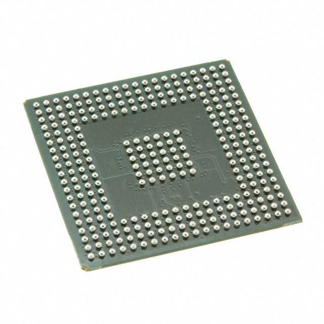
packaged in a leaded or lead-free 292-ball thermally
enhanced BGA package over the rated industrial
temperature range of -40°C to +85°C.
1
2
•
•
•
•
•
•
•
•
•
•
Excellent Accuracy and Dynamic Performance
Pin Compatible with ADC12D1000/1600/1800
Low Power Consumption, Further Reduced at
Lower Fs
Internally Terminated, Buffered, Differential
Analog Inputs
R/W SPI Interface for Extended Control Mode
Dual-Edge Sampling Mode, in Which the I- and
Q-channels Sample One Input at Twice the
Sampling Clock Rate
Test Patterns at Output for System Debug
Programmable 15-bit Gain and 12-bit Plus Sign
Offset
Programmable tAD Adjust Feature
1:1 Non-demuxed or 1:2 Demuxed LVDS
Outputs
AutoSync Feature for Multi-Chip Systems
Single 1.9V ± 0.1V Power Supply
292-Ball BGA Package (27mm x 27mm x
2.4mm with 1.27mm Ball-Pitch); No Heat Sink
Required
APPLICATIONS
•
•
•
Wideband Communications
Data Acquisition Systems
Digital Oscilloscopes
The ADC10D1000/1500 builds upon the features,
architecture and functionality of the 8-bit GHz family
of ADCs. An expanded feature set includes AutoSync
for multi-chip synchronization, 15-bit programmable
gain and 12-bit plus sign programmable offset
adjustment for each channel. The improved internal
track-and-hold amplifier and the extended selfcalibration scheme enable a very flat response of all
dynamic parameters beyond Nyquist, producing
9.1/9.0 Effective Number of Bits (ENOB) with a 100
MHz input signal and a 1.0/1.5 GHz sample rate
while providing a 10-18 Code Error Rate (CER)
Dissipating a typical 2.77/3.59 Watts in NonDemultiplex Mode at 1.0/1.5 GSPS from a single
1.9V supply, this device is specified to have no
missing codes over the full operating temperature
range.
Each channel has its own independent DDR Data
Clock, DCLKI and DCLKQ, which are in phase when
both channels are powered up, so that only one Data
Clock could be used to capture all data, which is sent
out at the same rate as the input sample clock. If the
1:2 Demux Mode is selected, a second 10-bit LVDS
bus becomes active for each channel, such that the
output data rate is sent out two times slower to relax
data-capture timing requirements. The part can also
be used as a single 2.0/3.0 GSPS ADC to sample
one of the I or Q inputs. The output formatting can be
programmed to be offset binary or two's complement
and the Low Voltage Differential Signaling (LVDS)
digital outputs are compatible with IEEE 1596.3-1996,
with the exception of an adjustable common mode
voltage between 0.8V and 1.2V to allow for power
reduction for well-controlled back planes.
1
2
Please be aware that an important notice concerning availability, standard warranty, and use in critical applications of
Texas Instruments semiconductor products and disclaimers thereto appears at the end of this data sheet.
All trademarks are the property of their respective owners.
PRODUCTION DATA information is current as of publication date.
Products conform to specifications per the terms of the Texas
Instruments standard warranty. Production processing does not
necessarily include testing of all parameters.
Copyright © 2008–2013, Texas Instruments Incorporated
�ADC10D1000, ADC10D1500
SNAS462Q – OCTOBER 2008 – REVISED MARCH 2013
www.ti.com
These devices have limited built-in ESD protection. The leads should be shorted together or the device placed in conductive foam
during storage or handling to prevent electrostatic damage to the MOS gates.
Table 1. Key Specifications
(Non-Demux Non-DES Mode, Fs=1.0/1.5 GSPS, Fin = 100 MHz)
Resolution
10 Bits
Conversion Rate
Dual channels at 1.0/1.5 GSPS (typ)
Single channel at 2.0/3.0 GSPS (typ)
Code Error Rate
10-18/10-18 (typ)
ENOB
9.1/9.0 bits (typ)
SNR
57/56.8 dB (typ)
SFDR
70/68 dBc (typ)
Full Power Bandwidth
2.8/2.8 GHz (typ)
DNL
±0.25/±0.25 LSB (typ)
Power Consumption
Single Channel Enabled
1.61/1.92 W (typ)
Dual Channels Enabled
2.77/3.59 W (typ)
Power Down Mode
6/6 mW (typ)
Table 2. Ordering Information (1) (2)
(1)
(2)
2
Industrial Temperature Range (–40°C < TA < 85°C)
Package
ADC10D1000/1500CIUT/NOPB
Lead-free 292-Ball BGA Thermally Enhanced Package
ADC10D1000/1500CIUT
Leaded 292-Ball BGA Thermally Enhanced Package
ADC10D1000/1500RB
Reference Board
For the most current package and ordering information, see the Package Option Addendum at the end of this document, or see the TI
website at www.ti.com.
If Military/Aerospace specified devices are required, please contact the TI Sales Office/Distributors for availability and specifications.
IBIS models are available at www.ti.com
Submit Documentation Feedback
Copyright © 2008–2013, Texas Instruments Incorporated
Product Folder Links: ADC10D1000 ADC10D1500
�ADC10D1000, ADC10D1500
www.ti.com
SNAS462Q – OCTOBER 2008 – REVISED MARCH 2013
Block Diagram
10
VinI+
10
Rterm
T/H
10- Bit
ADC
DI(9:0)
1:2
Demux
10
DId(9:0)
VinI-
DCLKI
M
ORI
RCOut1
Output
RCOut2
Buffers
ORQ
Clock
Management
and AutoSync
U
X
DCLKQ
10
VinQ+
10
Rterm
T/H
10- Bit
ADC
DQ(9:0)
1:2
Demux
10
DQd(9:0)
VinQCLK+
Rterm
Control/Status
and Other Logic
CLKRCLK+
Rterm
Control Pins
SPI
RCLK-
Figure 1. Simplified Block Diagram
Copyright © 2008–2013, Texas Instruments Incorporated
Product Folder Links: ADC10D1000 ADC10D1500
Submit Documentation Feedback
3
�ADC10D1000, ADC10D1500
SNAS462Q – OCTOBER 2008 – REVISED MARCH 2013
www.ti.com
Connection Diagram
1
2
3
4
5
6
7
8
A
GND
V_A
SDO
TPM
NDM
V_A
GND
V_E
B
Vbg
GND
ECEb
SDI
CalRun
V_A
GND
GND_E
C
Rtrim+
Vcmo
Rext+
SCSb
SCLK
V_A
NC
V_E
D
DNC
Rtrim-
Rext-
GND
GND
CAL
DNC
V_A
E
V_A
Tdiode+
DNC
F
V_A
GND
_TC
G
V_TC
H
11
12
13
14
15
16
17
18
19
20
V_DR
DId1+
GND_
DR
DId4+
V_DR
DId7+
GND_
DR
DId9+
DId9-
GND_
DR
A
RSV0-
DId0+
DId1-
DId3+
DId4-
DId6+
DId7-
DId8+
RSV2+ RSV3+
RSV3-
B
GND_E RSV1+
DId0-
DId2+
DId3-
DId5+
DId6-
DId8-
RSV2-
V_DR
DI0+
DI0-
C
V_DR
DId2-
GND_
DR
DId5-
V_DR
GND_
DR
V_DR
DI1+
DI2+
DI2-
D
GND
GND_
DR
DI1-
DI3+
DI3-
E
Tdiode-
DNC
GND_
DR
DI4+
DI4-
GND_
DR
F
GND
_TC
V_TC
V_TC
DI5+
DI5-
DI6+
DI6-
G
VinI+
V_TC
GND
_TC
V_A
GND
GND
GND
GND
GND
GND
DI7+
DI7-
DI8+
DI8-
H
J
VinI-
GND
_TC
V_TC
VbiasI
GND
GND
GND
GND
GND
GND
V_DR
DI9+
DI9-
V_DR
J
K
GND
VbiasI
V_TC
GND
_TC
GND
GND
GND
GND
GND
GND
ORI+
ORI-
DCLK
_I+
L
GND
VbiasQ
V_TC
GND
_TC
GND
GND
GND
GND
GND
GND
ORQ+
ORQ-
DCLK
_Q+
DCLK
_Q-
L
M
VinQ-
GND
_TC
V_TC
VbiasQ
GND
GND
GND
GND
GND
GND
GND_
DR
DQ9+
DQ9-
GND_
DR
M
N
VinQ+
V_TC
GND
_TC
V_A
GND
GND
GND
GND
GND
GND
DQ7+
DQ7-
DQ8+
DQ8-
N
P
V_TC
GND
_TC
V_TC
V_TC
DQ5+
DQ5-
DQ6+
DQ6-
P
R
V_A
GND
_TC
V_TC
V_TC
V_DR
DQ4+
DQ4-
V_DR
R
T
V_A
GND
_TC
GND
_TC
GND
V_DR
DQ1-
DQ3+
DQ3-
T
U
GND
_TC
CLK+
PDI
GND
GND
RCOut
_1-
DNC
V_A
V
CLK-
DCLK
_RST+
PDQ
CalDly
DES
RCOut
_2+
RCOut
_2-
V_E
W
DCLK
_RST-
GND
DNC
DDRPh RCLK-
V_A
GND
GND_E
Y
GND
V_A
FSR
RCLK+
RCOut
_1+
V_A
GND
V_E
1
2
3
4
6
7
8
5
9
10
GND_E RSV0+
V_E
V_A
RSV1-
DCLK
_I-
K
RSV7-
V_DR
DQd2-
GND_
DR
DQd5-
V_DR
V_DR
GND_
DR
DQ1+
DQ2+
DQ2-
U
GND_E RSV7+
DQd0-
DQd2+
DQd3-
DQd5+
DQd6-
DQd8-
RSV4-
GND_
DR
DQ0+
DQ0-
V
DQd0+
DQd1-
DQd3+
DQd4-
DQd6+
DQd7-
DQd8+ RSV4+ RSV5+
RSV5-
W
V_DR
DQd1+
GND_
DR
DQd4+
V_DR
DQd7+
GND_
DR
DQd9+
DQd9-
GND_
DR
Y
11
12
13
14
15
16
17
18
19
20
V_A
V_E
RSV6-
GND_E RSV6+
9
10
Figure 2. ADC10D1000/1500 Connection Diagram
NOTE
The center ground pins are for thermal dissipation and must be soldered to a
ground plane to ensure rated performance. See SUPPLY/GROUNDING, LAYOUT
AND THERMAL RECOMMENDATIONS for more information.
4
Submit Documentation Feedback
Copyright © 2008–2013, Texas Instruments Incorporated
Product Folder Links: ADC10D1000 ADC10D1500
�ADC10D1000, ADC10D1500
www.ti.com
SNAS462Q – OCTOBER 2008 – REVISED MARCH 2013
Ball Descriptions and Equivalent Circuits
Table 3. Analog Front-End and Clock Balls
Ball No.
Name
Equivalent Circuit
Description
VA
50k
AGND
H1/J1
N1/M1
VinI+/VinQ+/-
VCMO
100
Control from VCMO
VA
50k
AGND
Differential signal I- and Q-inputs. In the Non-Dual
Edge Sampling (Non-DES) Mode, each I- and Qinput is sampled and converted by its respective
channel with each positive transition of the CLK
input. In Non-ECM (Non-Extended Control Mode)
and DES Mode, both channels sample the I-input.
In Extended Control Mode (ECM), the Q-input
may optionally be selected for conversion in DES
Mode by the DEQ Bit (Addr: 0h, Bit 6).
Each I- and Q-channel input has an internal
common mode bias that is disabled when DCcoupled Mode is selected. Both inputs must be
either AC- or DC-coupled. The coupling mode is
selected by the VCMO Pin.
In Non-ECM, the full-scale range of these inputs is
determined by the FSR Pin; both I- and Qchannels have the same full-scale input range. In
ECM, the full-scale input range of the I- and Qchannel inputs may be independently set via the
Control Register (Addr: 3h and Addr: Bh). Note
that the high and low full-scale input range setting
in Non-ECM corresponds to the mid and minimum
full-scale input range in ECM.
The input offset may also be adjusted in ECM.
VA
U2/V1
50k
AGND
CLK+/-
VA
100
VBIAS
50k
Differential Converter Sampling Clock. In the NonDES Mode, the analog inputs are sampled on the
positive transitions of this clock signal. In the DES
Mode, the selected input is sampled on both
transitions of this clock. This clock must be ACcoupled.
AGND
VA
AGND
V2/W1
DCLK_RST+/-
100
VA
Differential DCLK Reset. A positive pulse on this
input is used to reset the DCLKI and DCLKQ
outputs of two or more ADC10D1000/1500s in
order to synchronize them with other
ADC10D1000/1500s in the system. DCLKI and
DCLKQ are always in phase with each other,
unless one channel is powered down, and do not
require a pulse from DCLK_RST to become
synchronized. The pulse applied here must meet
timing relationships with respect to the CLK input.
Although supported, this feature has been
superseded by AutoSync.
AGND
Copyright © 2008–2013, Texas Instruments Incorporated
Product Folder Links: ADC10D1000 ADC10D1500
Submit Documentation Feedback
5
�ADC10D1000, ADC10D1500
SNAS462Q – OCTOBER 2008 – REVISED MARCH 2013
www.ti.com
Table 3. Analog Front-End and Clock Balls (continued)
Ball No.
Name
Equivalent Circuit
Description
VA
VCMO
C2
200k
VCMO
Enable AC
Coupling
8 pF
GND
VA
B1
Common Mode Voltage Output or Signal Coupling
Select. If AC-coupled operation at the analog
inputs is desired, this pin should be held at logiclow level. This pin is capable of sourcing/ sinking
up to 100 µA. For DC-coupled operation, this pin
should be left floating or terminated into highimpedance. In DC-coupled Mode, this pin provides
an output voltage which is the optimal commonmode voltage for the input signal and should be
used to set the common-mode voltage of the
driving buffer.
Bandgap Voltage Output or LVDS Common-mode
Voltage Select. This pin provides a buffered
version of the bandgap output voltage and is
capable of sourcing/sinking 100 uA and driving a
load of up to 80 pF. Alternately, this pin may be
used to select the LVDS digital output commonmode voltage. If tied to logic-high, the 1.2V LVDS
common-mode voltage is selected; 0.8V is the
default.
VBG
GND
VA
C3/D3
Rext+/-
V
External Reference Resistor terminals. A 3.3 kΩ
±0.1% resistor should be connected between
Rext+/-. The Rext resistor is used as a reference
to trim internal circuits which affect the linearity of
the converter; the value and precision of this
resistor should not be compromised.
V
Input Termination Trim Resistor terminals. A 3.3
kΩ ±0.1% resistor should be connected between
Rtrim+/-. The Rtrim resistor is used to establish
the calibrated 100Ω input impedance of VinI, VinQ
and CLK. These impedances may be fine tuned
by varying the value of the resistor by a
corresponding percentage; however, the tuning
range and performance is not specified for such
an alternate value.
GND
VA
C1/D2
Rtrim+/-
GND
VA
Tdiode_P
E2/F3
GND
Tdiode+/-
VA
Temperature Sensor Diode Positive (Anode) and
Negative (Cathode) Terminals. This set of pins is
used for die temperature measurements. It has
not been fully characterized.
Tdiode_N
GND
6
Submit Documentation Feedback
Copyright © 2008–2013, Texas Instruments Incorporated
Product Folder Links: ADC10D1000 ADC10D1500
�ADC10D1000, ADC10D1500
www.ti.com
SNAS462Q – OCTOBER 2008 – REVISED MARCH 2013
Table 3. Analog Front-End and Clock Balls (continued)
Ball No.
Name
Equivalent Circuit
Description
VA
Y4/W5
50k
AGND
RCLK+/-
100
VA
VBIAS
50k
Reference Clock Input. When the AutoSync
feature is active, and the ADC10D1000/1500 is in
Slave Mode, the internal divided clocks are
synchronized with respect to this input clock. The
delay on this clock may be adjusted when
synchronizing multiple ADCs. This feature is
available in ECM via Control Register (Addr: Eh).
AGND
VA
100:
Y5/U6
V6/V7
100:
RCOut1+/RCOut2+/-
+
Reference Clock Output 1 and 2. These signals
provide a reference clock at a rate of CLK/4, when
enabled, independently of whether the ADC is in
Master or Slave Mode. They are used to drive the
RCLK of another ADC10D1000/1500, to enable
automatic synchronization for multiple ADCs
(AutoSync feature). The impedance of each trace
from RCOut1 and RCOut2 to the RCLK of another
ADC10D1000/1500 should be 100Ω differential.
Having two clock outputs allows the autosynchronization to propagate as a binary tree. Use
the DOC Bit (Addr: Eh, Bit 1) to enable/ disable
this feature; default is disabled.
A GND
Table 4. Control and Status Balls
Ball No.
Name
Equivalent Circuit
VA
V5
DES
GND
Description
Dual Edge Sampling (DES) Mode select. In the
Non-Extended Control Mode (Non-ECM), when
this input is set to logic-high, the DES Mode of
operation is selected, meaning that the VinI input
is sampled by both channels in a time-interleaved
manner. The VinQ input is ignored. When this
input is set to logic-low, the device is in Non-DES
Mode, i.e. the I- and Q-channels operate
independently. In the Extended Control Mode
(ECM), this input is ignored and DES Mode
selection is controlled through the Control Register
by the DES Bit (Addr: 0h, Bit 7); default is NonDES Mode operation.
VA
V4
Calibration Delay select. By setting this input logichigh or logic-low, the user can select the device to
wait a longer or shorter amount of time,
respectively, before the automatic power-on selfcalibration is initiated. This feature is pin-controlled
only and is always active during ECM and NonECM.
CalDly
GND
Copyright © 2008–2013, Texas Instruments Incorporated
Product Folder Links: ADC10D1000 ADC10D1500
Submit Documentation Feedback
7
�ADC10D1000, ADC10D1500
SNAS462Q – OCTOBER 2008 – REVISED MARCH 2013
www.ti.com
Table 4. Control and Status Balls (continued)
Ball No.
Name
Equivalent Circuit
VA
D6
CAL
GND
Description
Calibration cycle initiate. The user can command
the device to execute a self-calibration cycle by
holding this input high a minimum of tCAL_H after
having held it low a minimum of tCAL_L. If this input
is held high at the time of power-on, the automatic
power-on calibration cycle is inhibited until this
input is cycled low-then-high. This pin is active in
both ECM and Non-ECM. In ECM, this pin is
logically OR'd with the CAL Bit (Addr: 0h, Bit 15)
in the Control Register. Therefore, both pin and bit
must be set low and then either can be set high to
execute an on-command calibration.
VA
B5
Calibration Running indication. This output is
logic-high while the calibration sequence is
executing. This output is logic-low otherwise.
CalRun
GND
VA
50 k:
U3
V3
PDI
PDQ
GND
Power Down I- and Q-channel. Setting either input
to logic-high powers down the respective I- or Qchannel. Setting either input to logic-low brings the
respective I- or Q-channel to a operational state
after a finite time delay. This pin is active in both
ECM and Non-ECM. In ECM, each Pin is logically
OR'd with its respective Bit. Therefore, either this
pin or the PDI and PDQ Bit in the Control Register
can be used to power-down the I- and Q-channel
(Addr: 0h, Bit 11 and Bit 10), respectively.
VA
A4
Test Pattern Mode select. With this input at logichigh, the device continuously outputs a fixed,
repetitive test pattern at the digital outputs. In the
ECM, this input is ignored and the Test Pattern
Mode can only be activated through the Control
Register by the TPM Bit (Addr: 0h, Bit 12).
TPM
GND
VA
A5
Non-Demuxed Mode select. Setting this input to
logic-high causes the digital output bus to be in
the 1:1 Non-Demuxed Mode. Setting this input to
logic-low causes the digital output bus to be in the
1:2 Demuxed Mode. This feature is pin-controlled
only and remains active during ECM and NonECM.
NDM
GND
8
Submit Documentation Feedback
Copyright © 2008–2013, Texas Instruments Incorporated
Product Folder Links: ADC10D1000 ADC10D1500
�ADC10D1000, ADC10D1500
www.ti.com
SNAS462Q – OCTOBER 2008 – REVISED MARCH 2013
Table 4. Control and Status Balls (continued)
Ball No.
Name
Equivalent Circuit
VA
Y3
FSR
GND
VA
W4
DDRPh
GND
Description
Full-Scale input Range select. In Non-ECM, when
this input is set to logic-low or logic-high, the fullscale differential input range for both I- and Qchannel inputs is set to the lower or higher FSR
value, respectively. In the ECM, this input is
ignored and the full-scale range of the I- and Qchannel inputs is independently determined by the
setting of Addr: 3h and Addr: Bh, respectively.
Note that the high (lower) FSR value in Non-ECM
corresponds to the mid (min) available selection in
ECM; the FSR range in ECM is greater.
DDR Phase select. This input, when logic-low,
selects the 0° Data-to-DCLK phase relationship.
When logic-high, it selects the 90° Data-to-DCLK
phase relationship, i.e. the DCLK transition
indicates the middle of the valid data outputs. This
pin only has an effect when the chip is in 1:2
Demuxed Mode, i.e. the NDM pin is set to logiclow. In ECM, this input is ignored and the DDR
phase is selected through the Control Register by
the DPS Bit (Addr: 0h, Bit 14); the default is 0°
Mode.
VA
50 k:
B3
ECE
Extended Control Enable bar. Extended feature
control through the SPI interface is enabled when
this signal is asserted (logic-low). In this case,
most of the direct control pins have no effect.
When this signal is de-asserted (logic-high), the
SPI interface is disabled, all SPI registers are
reset to their default values, and all available
settings are controlled via the control pins.
GND
VA
100 k:
C4
SCS
Serial Chip Select bar. In ECM, when this signal is
asserted (logic-low), SCLK is used to clock in
serial data which is present on SDI and to source
serial data on SDO. When this signal is deasserted (logic-high), SDI is ignored and SDO is in
tri-stated.
GND
VA
100 k:
C5
SCLK
Serial Clock. In ECM, serial data is shifted into
and out of the device synchronously to this clock
signal. This clock may be disabled and held logiclow, as long as timing specifications are not
violated when the clock is enabled or disabled.
GND
Copyright © 2008–2013, Texas Instruments Incorporated
Product Folder Links: ADC10D1000 ADC10D1500
Submit Documentation Feedback
9
�ADC10D1000, ADC10D1500
SNAS462Q – OCTOBER 2008 – REVISED MARCH 2013
www.ti.com
Table 4. Control and Status Balls (continued)
Ball No.
Name
Equivalent Circuit
Description
VA
100 k:
B4
Serial Data-In. In ECM, serial data is shifted into
the device on this pin while SCS signal is asserted
(logic-low).
SDI
GND
VA
A3
Serial Data-Out. In ECM, serial data is shifted out
of the device on this pin while SCS signal is
asserted (logic-low). This output is tri-stated when
SCS is de-asserted.
SDO
GND
D1, D7, E3, F4,
W3, U7
DNC
NONE
Do Not Connect. These pins are used for internal
purposes and should not be connected, i.e. left
floating. Do not ground.
C7
NC
NONE
Not Connected. This pin is not bonded and may
be left floating or connected to any potential.
Table 5. Power and Ground Balls
Ball No.
Name
Equivalent Circuit
A2, A6, B6, C6,
D8, D9, E1, F1,
H4, N4, R1, T1,
U8, U9, W6, Y2,
Y6
VA
NONE
Power Supply for the Analog circuitry. This supply
is tied to the ESD ring. Therefore, it must be
powered up before or with any other supply.
G1, G3, G4, H2,
J3, K3, L3, M3,
N2, P1, P3, P4,
R3, R4
VTC
NONE
Power Supply for the Track-and-Hold and Clock
circuitry.
A11, A15, C18,
D11, D15, D17,
J17, J20, R17,
R20, T17, U11,
U15, U16, Y11,
Y15
VDR
NONE
Power Supply for the Output Drivers.
A8, B9, C8, V8,
W9, Y8
VE
NONE
Power Supply for the Digital Encoder.
NONE
Bias Voltage I-channel. This is an externally
decoupled bias voltage for the I-channel. Each pin
should individually be decoupled with a 100 nF
capacitor via a low resistance, low inductance
path to GND.
NONE
Bias Voltage Q-channel. This is an externally
decoupled bias voltage for the Q-channel. Each
pin should individually be decoupled with a 100 nF
capacitor via a low resistance, low inductance
path to GND.
J4, K2
L2, M4
10
VbiasI
VbiasQ
Submit Documentation Feedback
Description
Copyright © 2008–2013, Texas Instruments Incorporated
Product Folder Links: ADC10D1000 ADC10D1500
�ADC10D1000, ADC10D1500
www.ti.com
SNAS462Q – OCTOBER 2008 – REVISED MARCH 2013
Table 5. Power and Ground Balls (continued)
Ball No.
Name
Equivalent Circuit
A1, A7, B2, B7,
D4, D5, E4, K1,
L1, T4, U4, U5,
W2, W7, Y1, Y7,
H8:N13
Description
GND
NONE
Ground Return for the Analog circuitry.
F2, G2, H3, J2,
K4, L4, M2, N3,
P2, R2, T2, T3,
U1
GNDTC
NONE
Ground Return for the Track-and-Hold and Clock
circuitry.
A13, A17, A20,
D13, D16, E17,
F17, F20, M17,
M20, U13, U17,
V18, Y13, Y17,
Y20
GNDDR
NONE
Ground Return for the Output Drivers.
A9, B8, C9, V9,
W8, Y9
GNDE
NONE
Ground Return for the Digital Encoder.
Table 6. High-Speed Digital Outputs
Ball No.
Name
Equivalent Circuit
Description
VDR
K19/K20
L19/L20
DCLKI+/DCLKQ+/-
-
+
+
-
Data Clock Output for the I- and Q-channel data
bus. These differential clock outputs are used to
latch the output data and, if used, should always
be terminated with a 100Ω differential resistor
placed as closely as possible to the differential
receiver. Delayed and non-delayed data outputs
are supplied synchronously to this signal. In 1:2
Demux Mode or Non-Demux Mode, this signal is
at ¼ or ½ the sampling clock rate, respectively.
DCLKI and DCLKQ are always in phase with each
other, unless one channel is powered down, and
do not require a pulse from DCLK_RST to
become synchronized.
DR GND
VDR
K17/K18
L17/L18
ORI+/ORQ+/-
-
+
+
-
Out-of-Range Output for the I- and Q-channel.
This differential output is asserted logic-high while
the over- or under-range condition exists, i.e. the
differential signal at each respective analog input
exceeds the full-scale value. Each OR result
refers to the current Data, with which it is clocked
out. If used, each of these outputs should always
be terminated with a 100Ω differential resistor
placed as closely as possible to the differential
receiver.
DR GND
Copyright © 2008–2013, Texas Instruments Incorporated
Product Folder Links: ADC10D1000 ADC10D1500
Submit Documentation Feedback
11
�ADC10D1000, ADC10D1500
SNAS462Q – OCTOBER 2008 – REVISED MARCH 2013
www.ti.com
Table 6. High-Speed Digital Outputs (continued)
12
Ball No.
Name
J18/J19
H19/H20
H17/H18
G19/G20
G17/G18
F18/F19
E19/E20
D19/D20
D18/E18
C19/C20
·
M18/M19
N19/N20
N17/N18
P19/P20
P17/P18
R18/R19
T19/T20
U19/U20
U18/T18
V19/V20
DI9+/DI8+/DI7+/DI6+/DI5+/DI4+/DI3+/DI2+/DI1+/DI0+/·
DQ9+/DQ8+/DQ7+/DQ6+/DQ5+/DQ4+/DQ3+/DQ2+/DQ1+/DQ0+/-
A18/A19
B17/C16
A16/B16
B15/C15
C14/D14
A14/B14
B13/C13
C12/D12
A12/B12
B11/C11
·
Y18/Y19
W17/V16
Y16/W16
W15/V15
V14/U14
Y14/W14
W13/V13
V12/U12
Y12/W12
W11/V11
DId9+/DId8+/DId7+/DId6+/DId5+/DId4+/DId3+/DId2+/DId1+/DId0+/·
DQd9+/DQd8+/DQd7+/DQd6+/DQd5+/DQd4+/DQd3+/DQd2+/DQd1+/DQd0+/-
V10/U10
Y10/W10
W19/W20
W18/V17
B19/B20
B18/C17
C10/D10
A10/B10
RSV7+/RSV6+/RSV5+/RSV4+/RSV3+/RSV2+/RSV1+/RSV0+/-
Submit Documentation Feedback
Equivalent Circuit
Description
VDR
-
+
+
-
I- and Q-channel Digital Data Outputs. In NonDemux Mode, this LVDS data is transmitted at the
sampling clock rate. In Demux Mode, these
outputs provide ½ the data at ½ the sampling
clock rate, synchronized with the delayed data, i.e.
the other ½ of the data which was sampled one
clock cycle earlier. Compared with the DId and
DQd outputs, these outputs represent the later
time samples. If used, each of these outputs
should always be terminated with a 100Ω
differential resistor placed as closely as possible
to the differential receiver.
DR GND
VDR
-
+
+
-
Delayed I- and Q-channel Digital Data Outputs. In
Non-Demux Mode, these outputs are tri-stated. In
Demux Mode, these outputs provide ½ the data at
½ the sampling clock rate, synchronized with the
non-delayed data, i.e. the other ½ of the data
which was sampled one clock cycle later.
Compared with the DI and DQ outputs, these
outputs represent the earlier time samples. If
used, each of these outputs should always be
terminated with a 100Ω differential resistor placed
as closely as possible to the differential receiver.
DR GND
NONE
Reserved. These pins are used for internal
purposes. They may be left unconnected and
floating or connected as recommended in
Terminating RSV Pins.
Copyright © 2008–2013, Texas Instruments Incorporated
Product Folder Links: ADC10D1000 ADC10D1500
�ADC10D1000, ADC10D1500
www.ti.com
SNAS462Q – OCTOBER 2008 – REVISED MARCH 2013
Absolute Maximum Ratings
See notes
(1) (2)
Supply Voltage (VA, VTC, VDR, VE)
2.2V
Supply Difference
max(VA/TC/DR/E)min(VA/TC/DR/E)
0V to 100 mV
−0.15V to
(VA + 0.15V)
Voltage on Any Input Pin
(except VIN+/-)
VIN+/- Voltage Range
-0.15V to 2.5V
Ground Difference
max(GNDTC/DR/E)
-min(GNDTC/DR/E)
Input Current at Any Pin
0V to 100 mV
(3)
±50 mA
ADC10D1000 Package Power Dissipation at TA ≤ 85°C
(3)
3.7 W
ADC10D1500 Package Power Dissipation at TA ≤ 70°C
(3)
4.4 W
ESD Susceptibility (4)
Human Body Model
Charged Device Model
Machine Model
2500V
750V
250V
−65°C to +150°C
Storage Temperature
(1)
(2)
(3)
(4)
Absolute Maximum Ratings indicate limits beyond which damage to the device may occur. There is no assurance of operation at the
Absolute Maximum Ratings. For specifications and test conditions, see the Electrical Characteristics. The specifications apply only for
the test conditions listed. Some performance characteristics may degrade when the device is not operated under the listed test
conditions.
All voltages are measured with respect to GND = GNDTC = GNDDR = GNDE = 0V, unless otherwise specified.
When the input voltage at any pin exceeds the power supply limits, i.e. less than GND or greater than VA, the current at that pin should
be limited to 50 mA. In addition, over-voltage at a pin must adhere to the maximum voltage limits. Simultaneous over-voltage at multiple
pins requires adherence to the maximum package power dissipation limits. These dissipation limits are calculated using JEDEC
JESD51-7 thermal model. Higher dissipation may be possible based on specific customer thermal situation and specified package
thermal resistances from junction to case.
Human body model is 100 pF capacitor discharged through a 1.5 kΩ resistor. Machine model is 220 pF discharged through 0Ω.
Charged device model simulates a pin slowly acquiring charge (such as from a device sliding down the feeder in an automated
assembler) then rapidly being discharged.
Operating Ratings
See notes
(1) (2)
Ambient Temperature Range
ADC10D1000
−40°C ≤ TA ≤ +85°C
ADC10D1500 (Standard JEDEC thermal model)
−40°C ≤ TA ≤ +70°C
ADC10D1500 (Enhanced thermal model/heatsink)
−40°C ≤ TA ≤ +85°C
Junction Temperature Range
TJ ≤ +138°C
Supply Voltage (VA, VTC, VE)
+1.8V to +2.0V
Driver Supply Voltage (VDR)
+1.8V to VA
VIN+/- Voltage Range (Maintaining Common Mode)
0V to 2.15V
(100% duty cycle)
0V to 2.5V
(10% duty cycle)
Ground Difference
max(GNDTC/DR/E)
-min(GNDTC/DR/E)
0V
CLK+/- Voltage Range
0V to VA
Differential CLK Amplitude
0.4VP-P to 2.0VP-P
Common Mode Input Voltage
(1)
(2)
VCMO - 150mV < VCMI < VCMO +150mV
Operating Ratings indicate conditions for which the device is functional, but do not ensure specific performance limits. For specifications
and test conditions, see the Electrical Characteristics. The specifications apply only for the test conditions listed. Some performance
characteristics may degrade when the device is not operated under the listed test conditions.
All voltages are measured with respect to GND = GNDTC = GNDDR = GNDE = 0V, unless otherwise specified.
Copyright © 2008–2013, Texas Instruments Incorporated
Product Folder Links: ADC10D1000 ADC10D1500
Submit Documentation Feedback
13
�ADC10D1000, ADC10D1500
SNAS462Q – OCTOBER 2008 – REVISED MARCH 2013
www.ti.com
Package Thermal Resistance
Package
θJA
θJC1
θJC2
292-Ball BGA Thermally Enhanced Package
16°C/W
2.9°C/W
2.5°C/W
Converter Electrical Characteristics – Static Converter Characteristics
The following specifications apply after calibration for VA = VDR = VTC = VE = +1.9V; I- and Q-channels, AC-coupled, unused
channel terminated to AC ground, FSR Pin = High; CL = 10 pF; Differential, AC coupled Sine Wave Sampling Clock, fCLK =
1.0/1.5 GHz at 0.5 VP-P with 50% duty cycle (as specified); VBG = Floating; Non-Extended Control Mode; Rext = Rtrim =
3300Ω ± 0.1%; Analog Signal Source Impedance = 100Ω Differential; 1:2 Demultiplex Non-DES Mode; Duty Cycle Stabilizer
on. Boldface limits apply for TA = TMIN to TMAX. All other limits TA = 25°C, unless otherwise noted. (1) (2) (3) (4)
_
Symbol
Parameter
Conditions
ADC10D1000
ADC10D1500
Typ
Typ
Resolution with No Missing Codes
Lim
10
Lim
Units
(Limits)
10
bits
INL
Integral Non-Linearity
(Best fit)
1 MHz DC-coupled over-ranged
sine wave
±0.65
±1.4
±0.65
±1.4
LSB (max)
DNL
Differential Non-Linearity
1 MHz DC-coupled over-ranged
sine wave
±0.25
±0.5
±0.25
±0.55
LSB (max)
VOFF
Offset Error
VOFF_ADJ
Input Offset Adjustment Range
PFSE
Positive Full-Scale Error
(5)
NFSE
Negative Full-Scale Error
(5)
-2
Out-of-Range Output Code
(1)
(6)
Extended Control Mode
-2
±45
LSB
±45
±25
mV
±25
mV (max)
mV (max)
±25
±25
(VIN+) − (VIN−) > + Full Scale
1023
1023
(VIN+) − (VIN−) < − Full Scale
0
0
The analog inputs, labeled "I/O", are protected as shown below. Input voltage magnitudes beyond the Absolute Maximum Ratings may
damage this device.
V
A
TO INTERNAL
CIRCUITRY
I/O
GND
(2)
(3)
(4)
(5)
(6)
14
To specify accuracy, it is required that VA, VTC, VE and VDR be well-bypassed. Each supply pin must be decoupled with separate bypass
capacitors.
Typical figures are at TA = 25°C, and represent most likely parametric norms. Test limits are specified to AOQL (Average Outgoing
Quality Level).
The maximum clock frequency for Non-Demux Mode is tested up to 1.0 GHz for both the ADC10D1000 and the ADC10D1500 and
specified by design and characterization up to 1.5 GHz for the ADC10D1500.
Calculation of Full-Scale Error for this device assumes that the actual reference voltage is exactly its nominal value. Full-Scale Error for
this device, therefore, is a combination of Full-Scale Error and Reference Voltage Error. See Figure 4. For relationship between Gain
Error and Full-Scale Error, see Specification Definitions for Gain Error.
This parameter is specified by design and is not tested in production.
Submit Documentation Feedback
Copyright © 2008–2013, Texas Instruments Incorporated
Product Folder Links: ADC10D1000 ADC10D1500
�ADC10D1000, ADC10D1500
www.ti.com
SNAS462Q – OCTOBER 2008 – REVISED MARCH 2013
Converter Electrical Characteristics – Dynamic Converter Characteristics
The following specifications apply after calibration for VA = VDR = VTC = VE = +1.9V; I- and Q-channels, AC-coupled, unused
channel terminated to AC ground, FSR Pin = High; CL = 10 pF; Differential, AC coupled Sine Wave Sampling Clock, fCLK =
1.0/1.5 GHz at 0.5 VP-P with 50% duty cycle (as specified); VBG = Floating; Non-Extended Control Mode; Rext = Rtrim =
3300Ω ± 0.1%; Analog Signal Source Impedance = 100Ω Differential; 1:2 Demultiplex Non-DES Mode; Duty Cycle Stabilizer
on. Boldface limits apply for TA = TMIN to TMAX. All other limits TA = 25°C, unless otherwise noted. (1) (2) (3) (4)
_
Symbol
FPBW
Parameter
Conditions
Full Power Bandwidth
Gain Flatness
CER
Code Error Rate
NPR
Noise Power Ratio
ADC10D1000
ADC10D1500
Typ
Typ
Lim
Lim
Units
(Limits)
Non-DES Mode
2.8
2.8
GHz
DES Mode
1.25
1.25
GHz
DESIQ Mode
1.75
1.75
GHz
D.C. to Fs/2
±0.35
±0.4
dBFS
D.C. to Fs
±0.5
±1.2
-18
-18
10
dBFS
Error/Sam
ple
10
fc,notch = 325 MHz,
Notch width = 5%
48
48
dB
AIN = 100 MHz @ -0.5 dBFS
9.1
9.0
bits
AIN = 248 MHz @ -0.5 dBFS
9.1
1:2 Demux Non-DES Mode
ENOB
Effective Number of Bits
8.3
AIN = 373 MHz @ -0.5 dBFS
AIN = 498 MHz @ -0.5 dBFS
8.8
9.0
Signal-to-Noise Plus Distortion
Ratio
56.5
AIN = 248 MHz @ -0.5 dBFS
56.5
52
56
52
AIN = 373 MHz @ -0.5 dBFS
Signal-to-Noise Ratio
AIN = 100 MHz @ -0.5 dBFS
57
AIN = 248 MHz @ -0.5 dBFS
57
52.7
AIN = 373 MHz @ -0.5 dBFS
AIN = 498 MHz @ -0.5 dBFS
56.5
bits
56.1
dB
55.6
dB (min)
48.4
dB (min)
dB (min)
54.5
dB
56.8
dB
56.4
56.4
AIN = 748 MHz @ -0.5 dBFS
(1)
bits (min)
54.9
AIN = 748 MHz @ -0.5 dBFS
SNR
bits (min)
8.8
AIN = 100 MHz @ -0.5 dBFS
AIN = 498 MHz @ -0.5 dBFS
bits (min)
7.8
8.3
AIN = 748 MHz @ -0.5 dBFS
SINAD
8.9
52.7
dB (min)
50
dB (min)
dB (min)
55
dB
The analog inputs, labeled "I/O", are protected as shown below. Input voltage magnitudes beyond the Absolute Maximum Ratings may
damage this device.
V
A
TO INTERNAL
CIRCUITRY
I/O
GND
(2)
(3)
(4)
To specify accuracy, it is required that VA, VTC, VE and VDR be well-bypassed. Each supply pin must be decoupled with separate bypass
capacitors.
Typical figures are at TA = 25°C, and represent most likely parametric norms. Test limits are specified to AOQL (Average Outgoing
Quality Level).
The maximum clock frequency for Non-Demux Mode is tested up to 1.0 GHz for both the ADC10D1000 and the ADC10D1500 and
specified by design and characterization up to 1.5 GHz for the ADC10D1500.
Copyright © 2008–2013, Texas Instruments Incorporated
Product Folder Links: ADC10D1000 ADC10D1500
Submit Documentation Feedback
15
�ADC10D1000, ADC10D1500
SNAS462Q – OCTOBER 2008 – REVISED MARCH 2013
www.ti.com
Converter Electrical Characteristics – Dynamic Converter Characteristics (continued)
The following specifications apply after calibration for VA = VDR = VTC = VE = +1.9V; I- and Q-channels, AC-coupled, unused
channel terminated to AC ground, FSR Pin = High; CL = 10 pF; Differential, AC coupled Sine Wave Sampling Clock, fCLK =
1.0/1.5 GHz at 0.5 VP-P with 50% duty cycle (as specified); VBG = Floating; Non-Extended Control Mode; Rext = Rtrim =
3300Ω ± 0.1%; Analog Signal Source Impedance = 100Ω Differential; 1:2 Demultiplex Non-DES Mode; Duty Cycle Stabilizer
on. Boldface limits apply for TA = TMIN to TMAX. All other limits TA = 25°C, unless otherwise noted. (1) (2) (3) (4)
_
Symbol
THD
Parameter
Conditions
Total Harmonic Distortion
ADC10D1000
ADC10D1500
Typ
Typ
Lim
AIN = 100 MHz @ -0.5 dBFS
-67
AIN = 248 MHz @ -0.5 dBFS
-69
-60
-66
-60
AIN = 373 MHz @ -0.5 dBFS
AIN = 498 MHz @ -0.5 dBFS
Second Harmonic Distortion
dB
AIN = 248 MHz @ -0.5 dBFS
-71
-71
dBc
-71
dBc
-71
dBc
-70
dBc
AIN = 100 MHz @ -0.5 dBFS
-70
-68
dBc
AIN = 248 MHz @ -0.5 dBFS
-70
-72
dBc
-63
dBc
-69
dBc
AIN = 748 MHz @ -0.5 dBFS
-65
AIN = 100 MHz @ -0.5 dBFS
70
AIN = 248 MHz @ -0.5 dBFS
66
57.9
66
57.9
AIN = 373 MHz @ -0.5 dBFS
AIN = 498 MHz @ -0.5 dBFS
dBc
68
dBc
68
dBc (min)
63
AIN = 748 MHz @ -0.5 dBFS
ENOB
dB (max)
dBc
AIN = 498 MHz @ -0.5 dBFS
Non-Demux Non-DES Mode
54
dBc
(4)
Effective Number of Bits
AIN = 100 MHz @ -0.5 dBFS
9.1
AIN = 248 MHz @ -0.5 dBFS
9.1
AIN = 498 MHz @ -0.5 dBFS
8.4
9.1
bits
9.1
bits (min)
8.8
9.0
8.3
7.8
9.0
Signal-to-Noise Plus Distortion
Ratio
bits
AIN = 100 MHz @ -0.5 dBFS
56.6
AIN = 248 MHz @ -0.5 dBFS
56.5
56.5
52.6
AIN = 373 MHz @ -0.5 dBFS
AIN = 498 MHz @ -0.5 dBFS
56.5
54.5
56
52.0
dB
dB (min)
48.4
56
dB
AIN = 100 MHz @ -0.5 dBFS
57
AIN = 248 MHz @ -0.5 dBFS
57
53.5
AIN = 373 MHz @ -0.5 dBFS
AIN = 498 MHz @ -0.5 dBFS
57
dB
57
dB (min)
55.5
56.5
52.7
50
56.5
Total Harmonic Distortion
dB
AIN = 100 MHz @ -0.5 dBFS
-67
AIN = 248 MHz @ -0.5 dBFS
-66
-67
-60
-66
AIN = 748 MHz @ -0.5 dBFS
16
Submit Documentation Feedback
-60
dB
-66
−60
AIN = 373 MHz @ -0.5 dBFS
AIN = 498 MHz @ -0.5 dBFS
dB (min)
dB (min)
AIN = 748 MHz @ -0.5 dBFS
THD
dB (min)
dB (min)
AIN = 748 MHz @ -0.5 dBFS
Signal-to-Noise Ratio
bits (min)
bits (min)
AIN = 748 MHz @ -0.5 dBFS
SNR
dBc (min)
dBc (min)
65
AIN = 373 MHz @ -0.5 dBFS
SINAD
dB (max)
-76
AIN = 373 MHz @ -0.5 dBFS
Spurious-Free Dynamic Range
-53.6
-63
AIN = 748 MHz @ -0.5 dBFS
SFDR
dB (max)
-76
AIN = 498 MHz @ -0.5 dBFS
Third Harmonic Distortion
dB
-63
AIN = 100 MHz @ -0.5 dBFS
AIN = 373 MHz @ -0.5 dBFS
3rd Harm
Units
(Limits)
-65
-60
AIN = 748 MHz @ -0.5 dBFS
2nd Harm
Lim
-66
dB (max)
−53.6
dB (max)
dB (max)
dB
Copyright © 2008–2013, Texas Instruments Incorporated
Product Folder Links: ADC10D1000 ADC10D1500
�ADC10D1000, ADC10D1500
www.ti.com
SNAS462Q – OCTOBER 2008 – REVISED MARCH 2013
Converter Electrical Characteristics – Dynamic Converter Characteristics (continued)
The following specifications apply after calibration for VA = VDR = VTC = VE = +1.9V; I- and Q-channels, AC-coupled, unused
channel terminated to AC ground, FSR Pin = High; CL = 10 pF; Differential, AC coupled Sine Wave Sampling Clock, fCLK =
1.0/1.5 GHz at 0.5 VP-P with 50% duty cycle (as specified); VBG = Floating; Non-Extended Control Mode; Rext = Rtrim =
3300Ω ± 0.1%; Analog Signal Source Impedance = 100Ω Differential; 1:2 Demultiplex Non-DES Mode; Duty Cycle Stabilizer
on. Boldface limits apply for TA = TMIN to TMAX. All other limits TA = 25°C, unless otherwise noted. (1) (2) (3) (4)
_
Symbol
2nd Harm
Parameter
Conditions
Second Harmonic Distortion
ADC10D1000
ADC10D1500
Typ
Typ
Lim
Lim
Units
(Limits)
AIN = 100 MHz @ -0.5 dBFS
-85
-85
dBc
AIN = 248 MHz @ -0.5 dBFS
-71
-71
dBc
-71
-71
AIN = 100 MHz @ -0.5 dBFS
-68
-68
dBc
AIN = 248 MHz @ -0.5 dBFS
-70
-70
dBc
-70
-70
AIN = 373 MHz @ -0.5 dBFS
AIN = 498 MHz @ -0.5 dBFS
dBc
dBc
AIN = 748 MHz @ -0.5 dBFS
3rd Harm
Third Harmonic Distortion
dBc
AIN = 373 MHz @ -0.5 dBFS
AIN = 498 MHz @ -0.5 dBFS
dBc
dBc
AIN = 748 MHz @ -0.5 dBFS
SFDR
Spurious-Free Dynamic Range
dBc
AIN = 100 MHz @ -0.5 dBFS
68
AIN = 248 MHz @ -0.5 dBFS
66
59
66
57.9
AIN = 373 MHz @ -0.5 dBFS
AIN = 498 MHz @ -0.5 dBFS
68
dBc
66
dBc (min)
63
66
54
dBc (min)
dBc (min)
AIN = 748 MHz @ -0.5 dBFS
dBc
DES Mode (Demux and Non-Demux Modes, Q-input only)
ENOB
Effective Number of Bits
AIN = 100 MHz @ -0.5 dBFS
8.6
8.9
bits
AIN = 248 MHz @ -0.5 dBFS
8.5
8.7
bits
8.5
bits
AIN = 373 MHz @ -0.5 dBFS
AIN = 498 MHz @ -0.5 dBFS
8.4
AIN = 748 MHz @ -0.5 dBFS
SINAD
Signal-to-Noise Plus Distortion
Ratio
8.3
bits
AIN = 100 MHz @ -0.5 dBFS
53.6
55.5
dB
AIN = 248 MHz @ -0.5 dBFS
52.9
53.9
dB
52.7
dB
AIN = 373 MHz @ -0.5 dBFS
AIN = 498 MHz @ -0.5 dBFS
52.3
AIN = 748 MHz @ -0.5 dBFS
SNR
Signal-to-Noise Ratio
55.9
dB
AIN = 248 MHz @ -0.5 dBFS
53.3
54.6
dB
53.8
dB
52.7
AIN = 748 MHz @ -0.5 dBFS
52.1
dB
-67
-66
dB
AIN = 248 MHz @ -0.5 dBFS
-64
-62
dB
-59
dB
AIN = 498 MHz @ -0.5 dBFS
-63
AIN = 748 MHz @ -0.5 dBFS
Second Harmonic Distortion
dB
AIN = 100 MHz @ -0.5 dBFS
AIN = 373 MHz @ -0.5 dBFS
2nd Harm
dB
53.8
AIN = 498 MHz @ -0.5 dBFS
Total Harmonic Distortion
dB
51.7
AIN = 100 MHz @ -0.5 dBFS
AIN = 373 MHz @ -0.5 dBFS
THD
bits
dB
-62
dB
AIN = 100 MHz @ -0.5 dBFS
-77
-80
dBc
AIN = 248 MHz @ -0.5 dBFS
-66
-66
dBc
-64
dBc
AIN = 373 MHz @ -0.5 dBFS
AIN = 498 MHz @ -0.5 dBFS
-66
AIN = 748 MHz @ -0.5 dBFS
Copyright © 2008–2013, Texas Instruments Incorporated
Product Folder Links: ADC10D1000 ADC10D1500
dBc
-70
Submit Documentation Feedback
dBc
17
�ADC10D1000, ADC10D1500
SNAS462Q – OCTOBER 2008 – REVISED MARCH 2013
www.ti.com
Converter Electrical Characteristics – Dynamic Converter Characteristics (continued)
The following specifications apply after calibration for VA = VDR = VTC = VE = +1.9V; I- and Q-channels, AC-coupled, unused
channel terminated to AC ground, FSR Pin = High; CL = 10 pF; Differential, AC coupled Sine Wave Sampling Clock, fCLK =
1.0/1.5 GHz at 0.5 VP-P with 50% duty cycle (as specified); VBG = Floating; Non-Extended Control Mode; Rext = Rtrim =
3300Ω ± 0.1%; Analog Signal Source Impedance = 100Ω Differential; 1:2 Demultiplex Non-DES Mode; Duty Cycle Stabilizer
on. Boldface limits apply for TA = TMIN to TMAX. All other limits TA = 25°C, unless otherwise noted. (1) (2) (3) (4)
_
Symbol
3rd Harm
Parameter
Conditions
Third Harmonic Distortion
ADC10D1000
ADC10D1500
Typ
Typ
-69
-67
dBc
-65
-70
dBc
-62
dBc
-63
AIN = 748 MHz @ -0.5 dBFS
-62
dBc
59.3
67
dBc
AIN = 248 MHz @ -0.5 dBFS
58.9
62
dBc
60
dBc
AIN = 498 MHz @ -0.5 dBFS
57.4
AIN = 748 MHz @ -0.5 dBFS
Submit Documentation Feedback
dBc
AIN = 100 MHz @ -0.5 dBFS
AIN = 373 MHz @ -0.5 dBFS
18
Units
(Limits)
AIN = 248 MHz @ -0.5 dBFS
AIN = 498 MHz @ -0.5 dBFS
Spurious-Free Dynamic Range
Lim
AIN = 100 MHz @ -0.5 dBFS
AIN = 373 MHz @ -0.5 dBFS
SFDR
Lim
dBc
59
dBc
Copyright © 2008–2013, Texas Instruments Incorporated
Product Folder Links: ADC10D1000 ADC10D1500
�ADC10D1000, ADC10D1500
www.ti.com
SNAS462Q – OCTOBER 2008 – REVISED MARCH 2013
Converter Electrical Characteristics – Analog Input/Output and Reference Characteristics
The following specifications apply after calibration for VA = VDR = VTC = VE = +1.9V; I- and Q-channels, AC-coupled, unused
channel terminated to AC ground, FSR Pin = High; CL = 10 pF; Differential, AC coupled Sine Wave Sampling Clock, fCLK =
1.0/1.5 GHz at 0.5 VP-P with 50% duty cycle (as specified); VBG = Floating; Non-Extended Control Mode; Rext = Rtrim =
3300Ω ± 0.1%; Analog Signal Source Impedance = 100Ω Differential; 1:2 Demultiplex Non-DES Mode; Duty Cycle Stabilizer
on. Boldface limits apply for TA = TMIN to TMAX. All other limits TA = 25°C, unless otherwise noted. (1) (2) (3) (4)
_
Symbol
Parameter
Conditions
ADC10D1000
ADC10D1500
Typ
Typ
Lim
Lim
Units
(Limits)
Analog Inputs
VIN_FSR
Analog Differential Input Full Scale Non-Extended Control Mode
Range
FSR Pin Low
540
mVP-P
(min)
660
660
mVP-P
(max)
720
720
mVP-P
(min)
860
mVP-P
(max)
540
600
FSR Pin High
600
790
790
860
Extended Control Mode
CIN
RIN
FM(14:0) = 0000h
600
600
mVP-P
FM(14:0) = 4000h (default)
790
790
mVP-P
FM(14:0) = 7FFFh
980
980
mVP-P
Analog Input Capacitance,
Non-DES Mode (5)
Differential
0.02
0.02
pF
Each input pin to ground
1.6
1.6
pF
Analog Input Capacitance,
DES Mode (5)
Differential
0.08
0.08
pF
Each input pin to ground
2.2
2.2
pF
Differential Input Resistance
100
96
104
100
93
Ω (min)
107
Ω (max)
Common Mode Output
VCMO
Common Mode Output Voltage
TC_VCMO
Common Mode Output Voltage
Temperature Coefficient
VCMO_LVL
VCMO input threshold to set
DC-coupling Mode
CL_VCMO
Maximum VCMO Load Capacitance
(1)
ICMO = ±100 µA
ICMO = ±100 µA
1.25
1.15
1.35
1.25
1.15
V (min)
1.35
V (max)
38
38
ppm/°C
0.63
0.63
V
(5)
80
80
pF
The analog inputs, labeled "I/O", are protected as shown below. Input voltage magnitudes beyond the Absolute Maximum Ratings may
damage this device.
V
A
TO INTERNAL
CIRCUITRY
I/O
GND
(2)
(3)
(4)
(5)
To specify accuracy, it is required that VA, VTC, VE and VDR be well-bypassed. Each supply pin must be decoupled with separate bypass
capacitors.
Typical figures are at TA = 25°C, and represent most likely parametric norms. Test limits are specified to AOQL (Average Outgoing
Quality Level).
The maximum clock frequency for Non-Demux Mode is tested up to 1.0 GHz for both the ADC10D1000 and the ADC10D1500 and
specified by design and characterization up to 1.5 GHz for the ADC10D1500.
This parameter is specified by design and is not tested in production.
Copyright © 2008–2013, Texas Instruments Incorporated
Product Folder Links: ADC10D1000 ADC10D1500
Submit Documentation Feedback
19
�ADC10D1000, ADC10D1500
SNAS462Q – OCTOBER 2008 – REVISED MARCH 2013
www.ti.com
Converter Electrical Characteristics – Analog Input/Output and Reference
Characteristics (continued)
The following specifications apply after calibration for VA = VDR = VTC = VE = +1.9V; I- and Q-channels, AC-coupled, unused
channel terminated to AC ground, FSR Pin = High; CL = 10 pF; Differential, AC coupled Sine Wave Sampling Clock, fCLK =
1.0/1.5 GHz at 0.5 VP-P with 50% duty cycle (as specified); VBG = Floating; Non-Extended Control Mode; Rext = Rtrim =
3300Ω ± 0.1%; Analog Signal Source Impedance = 100Ω Differential; 1:2 Demultiplex Non-DES Mode; Duty Cycle Stabilizer
on. Boldface limits apply for TA = TMIN to TMAX. All other limits TA = 25°C, unless otherwise noted. (1) (2) (3) (4)
_
Symbol
Parameter
Conditions
ADC10D1000
ADC10D1500
Typ
Typ
Lim
Lim
Units
(Limits)
Bandgap Reference
VBG
Bandgap Reference Output
Voltage
IBG = ±100 µA
TC_VBG
Bandgap Reference Voltage
Temperature Coefficient
IBG = ±100 µA
CL_VBG
Maximum Bandgap Reference
load Capacitance
20
Submit Documentation Feedback
1.25
1.15
1.35
32
1.25
1.15
V (min)
1.35
V (max)
32
ppm/°C
(5)
80
80
pF
Copyright © 2008–2013, Texas Instruments Incorporated
Product Folder Links: ADC10D1000 ADC10D1500
�ADC10D1000, ADC10D1500
www.ti.com
SNAS462Q – OCTOBER 2008 – REVISED MARCH 2013
Converter Electrical Characteristics – I-Channel to Q-Channel Characteristics
The following specifications apply after calibration for VA = VDR = VTC = VE = +1.9V; I- and Q-channels, AC-coupled, unused
channel terminated to AC ground, FSR Pin = High; CL = 10 pF; Differential, AC coupled Sine Wave Sampling Clock, fCLK =
1.0/1.5 GHz at 0.5 VP-P with 50% duty cycle (as specified); VBG = Floating; Non-Extended Control Mode; Rext = Rtrim =
3300Ω ± 0.1%; Analog Signal Source Impedance = 100Ω Differential; 1:2 Demultiplex Non-DES Mode; Duty Cycle Stabilizer
on. Boldface limits apply for TA = TMIN to TMAX. All other limits TA = 25°C, unless otherwise noted. (1) (2) (3) (4)
_
Symbol
Parameter
Conditions
Offset Match
X-TALK
(1)
ADC10D1000
ADC10D1500
Typ
Typ
Lim
Lim
Units
(Limits)
2
2
LSB
Positive Full-Scale Match
Zero offset selected in
Control Register
2
2
LSB
Negative Full-Scale Match
Zero offset selected in
Control Register
2
2
LSB
Phase Matching (I, Q)
fIN = 1.0 GHz