ADC1173
www.ti.com
SNAS025F – FEBRUARY 1999 – REVISED APRIL 2013
ADC1173 8-Bit, 3-Volt, 15MSPS, 33mW A/D Converter
Check for Samples: ADC1173
FEATURES
DESCRIPTION
•
•
•
•
The ADC1173 is a low power, 15 MSPS analog-todigital converter that digitizes signals to 8 bits while
consuming just 33 mW of power (typ). The ADC1173
uses a unique architecture that achieves 7.6 Effective
Bits. Output formatting is straight binary coding.
1
2
Internal Sample-and-Hold Function
Single +3V Operation
Internal Reference Bias Resistors
Industry Standard Pinout
APPLICATIONS
•
•
•
•
•
•
•
•
Video Digitization
Digital Still Cameras
Set Top Boxes
Camcorders
Personal Computer Video
Digital Television
CCD Imaging
Electro-Optics
The excellent DC and AC characteristics of this
device, together with its low power consumption and
+3V single supply operation, make it ideally suited for
many
video,
imaging
and
communications
applications, including use in portable equipment.
Furthermore, the ADC1173 is resistant to latch-up
and the outputs are short-circuit proof. The top and
bottom of the ADC1173's reference ladder is
available for connections, enabling a wide range of
input possibilities.
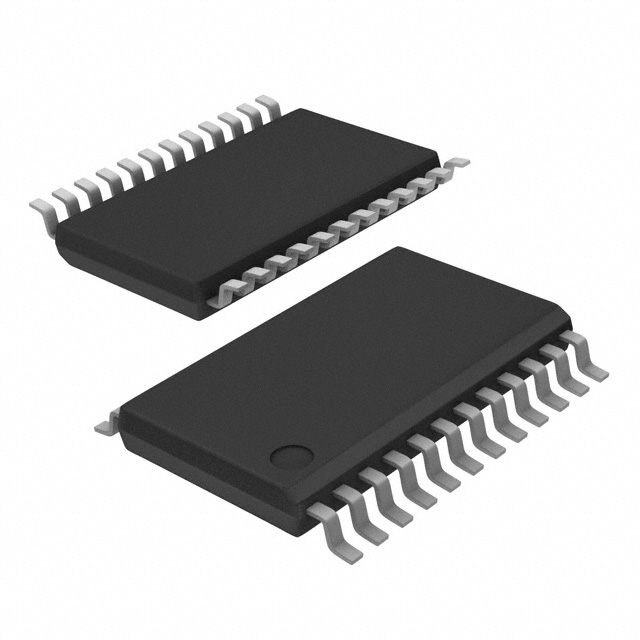
The ADC1173 is offered in a 24-pin TSSOP package
and is designed to operate over the -40°C to +75°C
commercial temperature range.
KEY SPECIFICATIONS
•
•
•
•
•
•
•
•
Resolution 8 Bits
Maximum Sampling Frequency 15 MSPS (min)
THD −54 dB (typ)
DNL ±0.85 LSB (max)
ENOB at 3.58 MHz Input 7.6 Bits (typ)
Differential Phase 0.5 Degree (max)
Differential Gain 1.5% (typ)
Power Consumption 33 mW (typ) (excluding
reference current)
PIN CONFIGURATION
Figure 1. 24-Pin TSSOP (Top View)
See PW Package
1
2
Please be aware that an important notice concerning availability, standard warranty, and use in critical applications of
Texas Instruments semiconductor products and disclaimers thereto appears at the end of this data sheet.
All trademarks are the property of their respective owners.
PRODUCTION DATA information is current as of publication date.
Products conform to specifications per the terms of the Texas
Instruments standard warranty. Production processing does not
necessarily include testing of all parameters.
Copyright © 1999–2013, Texas Instruments Incorporated
�ADC1173
SNAS025F – FEBRUARY 1999 – REVISED APRIL 2013
www.ti.com
BLOCK DIAGRAM
2
Submit Documentation Feedback
Copyright © 1999–2013, Texas Instruments Incorporated
Product Folder Links: ADC1173
�ADC1173
www.ti.com
SNAS025F – FEBRUARY 1999 – REVISED APRIL 2013
PIN DESCRIPTIONS AND EQUIVALENT CIRCUITS
Pin
No.
Symbol
Equivalent Circuit
Description
19
VIN
Analog signal input. Conversion range is VRB to VRT.
16
VRTS
Reference Top Bias with internal pull-up resistor. Short this
pin to VRT to self bias the reference ladder.
17
VRT
Analog Input that is the high (top) side of the reference ladder
of the ADC. Nominal range is 1.0V to AVDD. Voltage on VRT
and VRB inputs define the VIN conversion range. Bypass well.
For more information, see REFERENCE INPUTS.
23
VRB
Analog Input that is the low (bottom) side of the reference
ladder of the ADC. Nominal range is 0V to 2.0V. Voltage on
VRT and VRB inputs define the VIN conversion range. Bypass
well. For more information, see REFERENCE INPUTS.
22
VRBS
Reference Bottom Bias with internal pull down resistor. Short
to VRB to self bias the reference ladder.
Submit Documentation Feedback
Copyright © 1999–2013, Texas Instruments Incorporated
Product Folder Links: ADC1173
3
�ADC1173
SNAS025F – FEBRUARY 1999 – REVISED APRIL 2013
www.ti.com
PIN DESCRIPTIONS AND EQUIVALENT CIRCUITS (continued)
Pin
No.
Symbol
Equivalent Circuit
Description
1
OE
CMOS/TTL compatible Digital input that, when low, enables
the digital outputs of the ADC1173. When high, the outputs
are in a high impedance state.
12
CLK
CMOS/TTL compatible digital clock Input. VIN is sampled on
the falling edge of CLK input.
3 thru
10
D0-D7
Conversion data digital Output pins. D0 is the LSB, D7 is the
MSB. Valid data is output just after the rising edge of the CLK
input. These pins are enabled by bringing the OE pin low.
11, 13
DVDD
Positive digital supply pin. Connect to a clean, quiet voltage
source of +3V. AVDD and DVDD should have a common
source and be separately bypassed with a 10µF capacitor
and a 0.1µF ceramic chip capacitor. For more information,
see POWER SUPPLY CONSIDERATIONS.
2, 24
DVSS
The ground return for the digital supply. AVSS and DVSS
should be connected together close to the ADC1173.
14, 15,
18
AVDD
Positive analog supply pin. Connected to a clean, quiet
voltage source of +3V. AVDD and DVDD should have a
common source and be separately bypassed with a 10 µF
capacitor and a 0.1 µF ceramic chip capacitor. For more
information, see POWER SUPPLY CONSIDERATIONS.
20, 21
AVSS
The ground return for the analog supply. AVSS and DVSS
should be connected together close to the ADC1173
package.
These devices have limited built-in ESD protection. The leads should be shorted together or the device placed in conductive foam
during storage or handling to prevent electrostatic damage to the MOS gates.
4
Submit Documentation Feedback
Copyright © 1999–2013, Texas Instruments Incorporated
Product Folder Links: ADC1173
�ADC1173
www.ti.com
SNAS025F – FEBRUARY 1999 – REVISED APRIL 2013
ABSOLUTE MAXIMUM RATINGS (1) (2) (3)
AVDD, DVDD
6.5V
−0.3V to 6.5V
Voltage on Any Pin
VRT, VRB
AVDD to VSS
−0.5 to (AVDD + 0.5V)
CLK, OE Voltage
Digital Output Voltage
Input Current
DVSS to DVDD
(4)
±25mA
Package Input Current
(4)
±50mA
Package Dissipation at 25°C
ESD Susceptibility
(6)
See
Human Body Model
2000V
Machine Model
200V
Soldering Temp., Infrared, 10 sec.
300°C
−65°C to +150°C
Storage Temperature
(1)
(2)
(3)
(4)
(5)
(6)
(5)
Absolute Maximum Ratings indicate limits beyond which damage to the device may occur. Operating Ratings indicate conditions for
which the device is functional, but do not ensure specific performance limits. For ensured specifications and test conditions, see the
Electrical Characteristics. The ensured specifications apply only for the test conditions listed. Some performance characteristics may
degrade when the device is not operated under the listed test conditions.
All voltages are measured with respect to GND = AVSS = DVSS = 0V, unless otherwise specified.
If Military/Aerospace specified devices are required, please contact the Texas Instruments Sales Office/Distributors for availability and
specifications.
When the input voltage at any pin exceeds the power supplies (that is, less than AVSS or DVSS, or greater than AVDD or DVDD), the
current at that pin should be limited to 25 mA. The 50 mA maximum package input current rating limits the number of pins that can
safely exceed the power supplies with an input current of 25 mA to two.
The absolute maximum junction temperatures (TJmax) for this device is 150°C. The maximum allowable power dissipation is dictated by
TJmax, the junction-to-ambient thermal resistance θJA, and the ambient temperature, TA, and can be calculated using the formula
PDMAX = (TJmax - TA )/θJA. The power dissipation of this device under normal operation will typically be much lower than that required
to raise the junction temperature enough to be a problem. The values for maximum power dissipation listed above will be reached only
when the ADC1173 is operated in a severe fault condition (e.g. when input or output pins are driven beyond the power supply voltages,
or the power supply polarity is reversed). Obviously, such conditions should always be avoided.
Human body model is 100 pF capacitor discharged through a 1.5kΩ resistor. Machine model is 220 pF discharged through ZERO Ω.
OPERATING RATINGS (1) (2)
−40°C ≤ TA ≤ +75°C
Temperature Range
AVDD, DVDD
+2.7V to +3.6V
|AVSS -DVSS|
0V to 100 mV
VRT
1.0V to AVDD
VRB
0V to 2.0V
VRT - VRB
1.0V to 2.8V
VIN Voltage Range
(1)
(2)
VRB to VRT
Absolute Maximum Ratings indicate limits beyond which damage to the device may occur. Operating Ratings indicate conditions for
which the device is functional, but do not ensure specific performance limits. For ensured specifications and test conditions, see the
Electrical Characteristics. The ensured specifications apply only for the test conditions listed. Some performance characteristics may
degrade when the device is not operated under the listed test conditions.
All voltages are measured with respect to GND = AVSS = DVSS = 0V, unless otherwise specified.
Submit Documentation Feedback
Copyright © 1999–2013, Texas Instruments Incorporated
Product Folder Links: ADC1173
5
�ADC1173
SNAS025F – FEBRUARY 1999 – REVISED APRIL 2013
www.ti.com
CONVERTER ELECTRICAL CHARACTERISTICS
The following specifications apply for AVDD = DVDD = +3.0VDC, OE = 0V, VRT = +2.0V, VRB = 0V, CL = 20 pF, fCLK = 15MHz at
50% duty cycle. Boldface limits apply for TA = TMIN to TMAX; all other limits TA = 25°C (1) (2)
Symbol
Parameter
Conditions
Typical
(3)
Limits
Units
DC Accuracy
INL
Integral Non Linearity
±0.5
±1.3
LSB ( max)
DNL
Differential Non Linearity
±0.4
±0.85
LSB ( max)
0
(max)
Missing Codes
EOT
Top Offset
−12
mV
EOB
Bottom Offset
+1.0
mV
Video Accuracy
DP
Differential Phase Error
fin = 3.58 MHz sine wave
0.5
Degree
DG
Differential Gain Error
fin = 3.58 MHz sine wave
1.5
%
Analog Input and Reference Characteristics
V (min)
V (max)
Input Range
CIN
VIN Input Capacitance
RIN
Input Resistance
>1
MΩ
BW
Analog Input Bandwidth
120
MHz
RRT
Top Reference Resistor
360
RREF
Reference Ladder Resistance
RRB
Bottom Reference Resistor
IREF
Reference Ladder Current
2.0
VRB
VRT
VIN
VIN = 1.5V + 0.7Vrms
VRT to VRB
4
11
300
pF
Ω
200
Ω (min)
400
Ω (max)
90
Ω
VRT =VRTS, VRB =VRBS
4.2
mA
VRT =VRTS,VRB =AVSS
4.8
VRT
VRT connected to VRTS
Reference Top Self Bias Voltage
VRB connected to VRBS
VRB
Reference Bottom Self Bias
Voltage
(1)
(CLK LOW)
(CLK HIGH)
VRT connected to VRTS
VRB connected to VRBS
1.56
0.36
mA
1.45
1.65
V (min)
V (max)
0.32
V (min)
0.40
V (max)
The analog inputs are protected as shown below. Input voltage magnitudes up to 6.5V or to 500 mV below GND will not damage this
device. However, errors in the A/D conversion can occur if the input goes above VDD or below GND by more than 50 mV. As an
example, if AVDD is 2.7VDC, the full-scale input voltage must be ≤2.75VDC to ensure accurate conversions.
addf
addf
(2)
(3)
6
To ensure accuracy, it is required that AVDD and DVDD be well bypassed. Each supply pin must be decoupled with separate bypass
capacitors.
Typical figures are at TJ = 25°C, and represent most likely parametric norms. Test limits are ensured to TI's AOQL (Average Outgoing
Quality Level).
Submit Documentation Feedback
Copyright © 1999–2013, Texas Instruments Incorporated
Product Folder Links: ADC1173
�ADC1173
www.ti.com
SNAS025F – FEBRUARY 1999 – REVISED APRIL 2013
CONVERTER ELECTRICAL CHARACTERISTICS (continued)
The following specifications apply for AVDD = DVDD = +3.0VDC, OE = 0V, VRT = +2.0V, VRB = 0V, CL = 20 pF, fCLK = 15MHz at
50% duty cycle. Boldface limits apply for TA = TMIN to TMAX; all other limits TA = 25°C (1) (2)
Symbol
Parameter
VRTS VRBS
Self Bias Voltage Delta
VRT - VRB
Reference Voltage Delta
Conditions
Typical
VRT connected to VRTS,
VRB connected to VRBS
1.2
VRT connected to VRTS,
VRB connected to VSS
1.38
2
(3)
Limits
Units
1.1
1.3
µA (min)
µA (max)
V
1.0
V (min)
VA
V (max)
Power Supply Characteristics
IADD
Analog Supply Current
DVDD = AVDD = 3.6V
6.8
IDDD
Digital Supply Current
DVDD = AVDD = 3.6V
2.3
DVDD AVDD = 3.6V,
9.1
IAVDD +
IDVDD
Total Operating Current
Power Consumption
DVDD = AVDD = 3.6V, CLK Low
(4)
DVDD = AVDD = 3.6V
mA
mA
11.4
mA
41
mW
5.8
33
mA
CLK, OE Digital Input Characteristics
VIH
Logical High Input Voltage
DVDD = AVDD = 3.6V
2.2
V (min)
VIL
Logical Low Input Voltage
DVDD = AVDD = 3.6V
0.8
V (max)
IIH
Logical High Input Current
VIH = DVDD = AVDD = 3.6V
5
µA
IIL
Logic Low Input Current
VIL = 0V, DVDD = AVDD = 3.6V
−5
µA
CIN
Logic Input Capacitance
5
pF
Digital Output Characteristics
DVDD = 2.7V, IOH = −360µA
2.4
DVDD = 2.7V, IOH = −1.1mA
2.1
1.9
V (min)
Low Level Output Voltage
DVDD = 2.7V, IOL = 1.6mA
0.32
0.6
V (max)
TRI-STATE Leakage Current
DVDD = 3.6V, OE = DVDD,
VOL
= 0V or VOH = DVDD
±20
VOH
High Level Output Voltage
VOL
IOZH,
IOZL
V (min)
µA
AC Electrical Characteristics
fC1
Maximum Conversion Rate
20
fC2
Minimum Conversion Rate
1
MHz
28
ns
tOD
Output Delay
CLK rise to data rising
CLK rise to data falling
Pipeline Delay (Latency)
MHz (min)
24
ns
2.5
Clock Cycles
3
ns
tDS
Sampling (Aperture) Delay
tAJ
Aperture Jitter
30
ps rms
tOH
Output Hold Time
CLK high to data invalid
15
ns
tEN
OE Low to Data Valid
Loaded as in Figure 25
22
ns
tDIS
OE High to High Z State
Loaded as in Figure 25
12
ns
ENOB
Effective Number of Bits
fIN = 1.31 MHz
fIN = 3.58 MHz
fIN = 7.5 MHz
7.7
7.6
7.4
7.0
Bits (min)
SINAD
Signal-to- Noise & Distortion
fIN = 1.31 MHz
fIN = 3.58 MHz
fIN = 7.5 MHz
49
47.7
46.5
43
dB (min)
SNR
Signal-to-Noise Ratio
fIN = 1.31 MHz
fIN = 3.58 MHz
fIN = 7.5 MHz
49
48.7
48.0
44
dB (min)
SFDR
Spurious Free Dynamic Range
fIN = 1.31 MHz
fIN = 3.58 MHz
fIN = 7.5 MHz
65
55
51
(4)
CLK low to acquisition of data
15
dB
At least two clock cycles must be presented to the ADC1173 after power up. For details, see THE ADC1173 CLOCK.
Submit Documentation Feedback
Copyright © 1999–2013, Texas Instruments Incorporated
Product Folder Links: ADC1173
7
�ADC1173
SNAS025F – FEBRUARY 1999 – REVISED APRIL 2013
www.ti.com
CONVERTER ELECTRICAL CHARACTERISTICS (continued)
The following specifications apply for AVDD = DVDD = +3.0VDC, OE = 0V, VRT = +2.0V, VRB = 0V, CL = 20 pF, fCLK = 15MHz at
50% duty cycle. Boldface limits apply for TA = TMIN to TMAX; all other limits TA = 25°C (1) (2)
Symbol
THD
8
Parameter
Total Harmonic Distortion
Conditions
fIN = 1.31 MHz
fIN = 3.58 MHz
fIN = 7.5 MHz
Submit Documentation Feedback
Typical
−62
−54
−51
(3)
Limits
Units
dB
Copyright © 1999–2013, Texas Instruments Incorporated
Product Folder Links: ADC1173
�ADC1173
www.ti.com
SNAS025F – FEBRUARY 1999 – REVISED APRIL 2013
TYPICAL PERFORMANCE CHARACTERISTICS
INL vs. Temperature
DNL vs. Temperature
Figure 2.
Figure 3.
SNR vs. Temperature
SNR vs. fIN
Figure 4.
Figure 5.
THD vs. Temperature
SINAD vs. Temperature
Figure 6.
Figure 7.
Submit Documentation Feedback
Copyright © 1999–2013, Texas Instruments Incorporated
Product Folder Links: ADC1173
9
�ADC1173
SNAS025F – FEBRUARY 1999 – REVISED APRIL 2013
www.ti.com
TYPICAL PERFORMANCE CHARACTERISTICS (continued)
10
SINAD vs. fIN
SFDR vs. Temperature
Figure 8.
Figure 9.
SFDR vs. fIN
Differential Gain vs. Temperature
Figure 10.
Figure 11.
Differential Phase vs. Temperature
SNR vs. fIN
Figure 12.
Figure 13.
Submit Documentation Feedback
Copyright © 1999–2013, Texas Instruments Incorporated
Product Folder Links: ADC1173
�ADC1173
www.ti.com
SNAS025F – FEBRUARY 1999 – REVISED APRIL 2013
TYPICAL PERFORMANCE CHARACTERISTICS (continued)
THD vs. fIN
SINAD vs. fIN
Figure 14.
Figure 15.
SFDR vs. fIN
SNR vs. SUPPLY VOLTAGE
Figure 16.
Figure 17.
THD vs. SUPPLY VOLTAGE
SINAD vs. SUPPLY VOLTAGE
Figure 18.
Figure 19.
Submit Documentation Feedback
Copyright © 1999–2013, Texas Instruments Incorporated
Product Folder Links: ADC1173
11
�ADC1173
SNAS025F – FEBRUARY 1999 – REVISED APRIL 2013
www.ti.com
TYPICAL PERFORMANCE CHARACTERISTICS (continued)
12
SFDR vs. SUPPLY VOLTAGE
IDDD + IADD vs. fCLK
Figure 20.
Figure 21.
TOD vs. Temperature
Spectral Response
Figure 22.
Figure 23.
Submit Documentation Feedback
Copyright © 1999–2013, Texas Instruments Incorporated
Product Folder Links: ADC1173
�ADC1173
www.ti.com
SNAS025F – FEBRUARY 1999 – REVISED APRIL 2013
SPECIFICATION DEFINITIONS
ANALOG INPUT BANDWIDTH is a measure of the frequency at which the reconstructed output fundamental
drops 3 dB below its low frequency value for a full scale input. The test is performed with fIN equal to 100 kHz
plus integer multiples of fCLK. The input frequency at which the output is −3 dB relative to the low frequency input
signal is the full power bandwidth.
APERTURE JITTER is the time uncertainty of the sampling point (tDS), or the range of variation in the sampling
delay.
BOTTOM OFFSET is the difference between the input voltage that just causes the output code to transition to
the first code and the negative reference voltage. Bottom offset is defined as EOB = VZT - VRB, where VZT is the
first code transition input voltage. Note that this is different from the normal Zero Scale Error.
DIFFERENTIAL GAIN ERROR is the percentage difference between the output amplitudes of a high frequency
reconstructed sine wave at two different DC levels.
DIFFERENTIAL NON-LINEARITY (DNL) is the measure of the maximum deviation from the ideal step size of 1
LSB.
DIFFERENTIAL PHASE ERROR is the difference in the output phase of a reconstructed small signal sine wave
at two different DC levels.
EFFECTIVE NUMBER OF BITS (ENOB, or EFFECTIVE BITS) is another method of specifying Signal-to-Noise
and Distortion Ratio, or SINAD. ENOB is defined as (SINAD - 1.76) / 6.02 and says that the converter is
equivalent to a perfect ADC of this (ENOB) number of bits.
INTEGRAL NON-LINEARITY (INL) is a measure of the deviation of each individual code from a line drawn from
zero scale (½LSB below the first code transition) through positive full scale (½LSB above the last code
transition). The deviation of any given code from this straight line is measured from the center of that code value.
The end point test method is used.
OUTPUT DELAY is the time delay after the rising edge of the input clock before the data update is present at the
output pins.
OUTPUT HOLD TIME is the length of time that the output data is valid after the rise of the input clock.
PIPELINE DELAY (LATENCY) is the number of clock cycles between initiation of conversion and the availability
of that conversion result at the output. New data is available at every clock cycle, but the data lags the
conversion by the pipeline delay.
SAMPLING (APERTURE) DELAY is that time required after the fall of the clock input for the sampling switch to
open. The Sample/Hold circuit effectively stops capturing the input signal and goes into the "hold" mode tDS after
the clock goes low.
SIGNAL TO NOISE RATIO (SNR) is the ratio of the rms value of the input signal to the rms value of the other
spectral components below one-half the sampling frequency, not including harmonics or DC.
SIGNAL TO NOISE PLUS DISTORTION (S/(N+D) or SINAD) Is the ratio of the rms value of the input signal to
the rms value of all of the other spectral components below half the clock frequency, including harmonics but
excluding DC.
SPURIOUS FREE DYNAMIC RANGE (SFDR) is the difference, expressed in dB, between the rms values of the
input signal and the peak spurious signal, where a spurious signal is any signal present in the output spectrum
that is not present at the input.
TOP OFFSET is the difference between the positive reference voltage and the input voltage that just causes the
output code to transition to full scale and is defined as EOT = VFT − VRT. Where VFT is the full scale transition
input voltage. Note that this is different from the normal Full Scale Error.
TOTAL HARMONIC DISTORTION (THD) is the ratio of the rms total of the first six harmonic components, to the
rms value of the input signal.
Submit Documentation Feedback
Copyright © 1999–2013, Texas Instruments Incorporated
Product Folder Links: ADC1173
13
�ADC1173
SNAS025F – FEBRUARY 1999 – REVISED APRIL 2013
www.ti.com
Timing Diagram
Figure 24. Timing Diagram
Figure 25. tEN , tDIS Test Circuit
14
Submit Documentation Feedback
Copyright © 1999–2013, Texas Instruments Incorporated
Product Folder Links: ADC1173
�ADC1173
www.ti.com
SNAS025F – FEBRUARY 1999 – REVISED APRIL 2013
FUNCTIONAL DESCRIPTION
The ADC1173 uses a new, unique architecture to achieve 7.4 effective bits at and maintains superior dynamic
performance up to ½ the clock frequency.
The analog signal at VIN that is within the voltage range set by VRT and VRB are digitized to eight bits at up to 20
MSPS. Input voltages below VRB will cause the output word to consist of all zeroes. Input voltages above VRT will
cause the output word to consist of all ones. VRT has a range of 1.0 Volt to the analog supply voltage, AVDD,
while VRB has a range of 0 to 2.0 Volts. VRT should always be at least 1.0 Volt more positive than VRB.
If VRT and VRTS are connected together and VRB and VRBS are connected together, the nominal values of VRT and
VRB are 1.56V and 0.36V, respectively. If VRT and VRTS are connected together and VRB is grounded, the nominal
value of VRT is 1.38V.
Data is acquired at the falling edge of the clock and the digital equivalent of the data is available at the digital
outputs the pipeline delay (2.5 clock cycles) plus tOD later. The ADC1173 will convert as long as the clock signal
is present at pin 12. The Output Enable pin OE, when low, enables the output pins. The digital outputs are in the
high impedance state when the OE pin is high.
Submit Documentation Feedback
Copyright © 1999–2013, Texas Instruments Incorporated
Product Folder Links: ADC1173
15
�ADC1173
SNAS025F – FEBRUARY 1999 – REVISED APRIL 2013
www.ti.com
APPLICATIONS INFORMATION
THE ANALOG INPUT
The analog input of the ADC1173 is a switch followed by an integrator. The input capacitance changes with the
clock level, appearing as 4 pF when the clock is low, and 11 pF when the clock is high. Since a dynamic
capacitance is more difficult to drive than a fixed capacitance, choose an amplifier that can drive this type of load.
The LMH6702, LMH6609, LM6152, LM6154, LM6181 and LM6182 have been found to be excellent devices for
driving the ADC1173. Do not drive the input beyond the supply rails.
shows an example of an input circuit using the LM6181. This circuit has both gain and offset adjustments. If you
desire to eliminate these adjustments, you should reduce the signal swing to avoid clipping at the ADC1173
output that can result from normal tolerances of all system components. With no adjustments, the nominal value
for the amplifier feedback resistor is 510Ω and the 5.1k resistor at the inverting input should be changed to 860Ω
and returned to +3V rather than to the Offset Adjust potentiometer.
Driving the analog input with input signals up to 2.8VP-P will result in normal behavior where voltages above VRT
will result in a code of FFh and input voltages below VRB will result in an output code of zero. Input signals above
2.8V P-P may result in odd behavior where the output code is not FFh when the input exceeds VRT.
REFERENCE INPUTS
The reference inputs VRT (Reference Top) and VRB (Reference Bottom) are the top and bottom of the reference
ladder. Input signals between these two voltages will be digitized to 8 bits. External voltages applied to the
reference input pins should be within the range specified in the Operating Ratings table (1.0V to AVDD for VRT
and 0V to (AVDD - 1.0V) for VRB). Any device used to drive the reference pins should be able to source sufficient
current into the VRT pin and sink sufficient current from the VRB pin.
The reference ladder can be self-biased by connecting VRT to VRTS and connecting VRB to VRBS to provide top
and bottom reference voltages of approximately 1.56V and 0.36V, respectively, with VCC = 3.0V. This connection
is shown in Figure 26. If VRT and VRTS are tied together, but VRB is tied to analog ground, a top reference voltage
of approximately 1.38V is generated. The top and bottom of the ladder should be bypassed with 10µF tantalum
capacitors located close to the reference pins.
16
Submit Documentation Feedback
Copyright © 1999–2013, Texas Instruments Incorporated
Product Folder Links: ADC1173
�ADC1173
www.ti.com
SNAS025F – FEBRUARY 1999 – REVISED APRIL 2013
Because of resistor tolerances, the reference voltages can vary by as much as 6%. Choose an amplifier that can
drive a dynamic capacitance (see text).
Figure 26. Simple, Low Component Count, Self -Bias Reference application.
The reference self-bias circuit of is very simple and performance is adequate for many applications. Superior
performance can generally be achieved by driving the reference pins with a low impedance source.
By forcing a little current into or out of the top and bottom of the ladder, as shown in , the top and bottom
reference voltages can be trimmed. The resistive divider at the amplifier inputs can be replaced with
potentiometers. The LMC662 amplifier shown was chosen for its low offset voltage and low cost. Note that a
negative power supply is needed for these amplifiers if their outputs are required to go slightly negative to force
the required reference voltages.
Submit Documentation Feedback
Copyright © 1999–2013, Texas Instruments Incorporated
Product Folder Links: ADC1173
17
�ADC1173
SNAS025F – FEBRUARY 1999 – REVISED APRIL 2013
www.ti.com
Self-bias is still used, but the reference voltages are trimmed by providing a small trim current with the operational
amplifiers.
Figure 27. Better defining the ADC Reference Voltage.
18
Submit Documentation Feedback
Copyright © 1999–2013, Texas Instruments Incorporated
Product Folder Links: ADC1173
�ADC1173
www.ti.com
SNAS025F – FEBRUARY 1999 – REVISED APRIL 2013
Driving the reference to force desired values requires driving with a low impedance source, provided by the
transistors. Note that pins 16 and 22 are not connected.
Figure 28. Driving with a low impedance source
If reference voltages are desired that are more than a few tens of millivolts from the self-bias values, the circuit of
will allow forcing the reference voltages to whatever levels are desired. This circuit provides the best
performance because of the low source impedance of the transistors. Note that the VRTS and VRBS pins are left
floating.
VRT can be anywhere between VRB + 1.0V and the analog supply voltage, and VRB can be anywhere between
ground and 1.0V below VRT. To minimize noise effects and ensure accurate conversions, the total reference
voltage range (VRT - VRB) should be a minimum of 1.0V and a maximum of about VA. Best performance can be
realized with VRT= 1.56 and VRB= 0.36V. If VRB is not required to be below about +700mV, the -5V points in can
be returned to ground and the negative supply eliminated.
POWER SUPPLY CONSIDERATIONS
Many A/D converters draw sufficient transient current to corrupt their own power supplies if not adequately
bypassed. A 10µF tantalum or aluminum electrolytic capacitor should be placed within an inch (2.5 centimeters)
of the A/D power pins, with a 0.1 µF ceramic chip capacitor placed as close as possible to the converter's power
supply pins. Leadless chip capacitors are preferred because they have low lead inductance.
While a single voltage source should be used for the analog and digital supplies of the ADC1173, these supply
pins should be well isolated from each other to prevent any digital noise from being coupled to the analog power
pins. A 47 Ohm resistor is recommend between the analog and digital supply lines, with a ceramic capacitor
close to the analog supply pin. Avoid inductive components in the analog supply line.
The converter digital supply should not be the supply that is used for other digital circuitry on the board. It should
be the same supply used for the A/D analog supply.
Submit Documentation Feedback
Copyright © 1999–2013, Texas Instruments Incorporated
Product Folder Links: ADC1173
19
�ADC1173
SNAS025F – FEBRUARY 1999 – REVISED APRIL 2013
www.ti.com
As is the case with all high speed converters, the ADC1173 should be assumed to have little a.c. power supply
rejection, especially when self-biasing is used by connecting VRT and VRTS together.
No pin should ever have a voltage on it that is in excess of the supply voltages or below ground, not even on a
transient basis. This can be a problem upon application of power to a circuit. Be sure that the supplies to circuits
driving the CLK, OE, analog input and reference pins do not come up any faster than does the voltage at the
ADC1173 power pins.
Pins 11 and 13 are both labeled DVDD. Pin 11 is the supply point for the digital core of the ADC, where pin 13 is
used only to provide power to the ADC output drivers. As such, pin 11 may be connected to a voltage source
that is less than the +5V used for AVDD and DVDD to ease interfacing to low voltage devices. Pin 11 should never
exceed the pin 13 potential by more than 0.5V. Note that tOD will increase for lower pin 11 voltages.
THE ADC1173 CLOCK
Although the ADC1173 is tested and its performance is ensured with a 15MHz clock, it typically will function with
clock frequencies from 1MHz to 20MHz.
If continuous conversions are not required, power consumption can be reduced somewhat by stopping the clock
at a logic low when the ADC1173 is not being used. This reduces the current drain in the ADC1173's digital
circuitry from a typical value of 2.3mA to about 100µA.
Note that powering up the ADC1173 without the clock running may not save power, as it will result in an
increased current flow (by as much as 170%) in the reference ladder. In some cases, this may increase the
ladder current above the specified limit. Toggling the clock twice at 1MHz or higher and returning it to the low
state will eliminate the excess ladder current.
An alternative power-saving technique is to power up the ADC1173 with the clock active, then halt the clock in
the low state after two or more clock cycles. Stopping the clock in the high state is not recommended as a
power-saving technique.
LAYOUT AND GROUNDING
Proper grounding and proper routing of all signals is essential to ensure accurate conversion. Separate analog
and digital ground planes that are connected beneath the ADC1173 may be used, but best EMI practices require
a single ground plane. However, it is important to keep analog signal lines away from digital signal lines and
away from power supply currents. This latter requirement requires the careful separation and placement of power
planes. The use of power traces rather than one or more power planes is not recommended as higher
frequencies are not well filtered with lumped capacitances. To filter higher frequency noise, it is necessary to
have sufficient capacitance between the power and ground planes.
If separate analog and digital ground planes are used, the analog and digital grounds should be in the same
layer, but should be separated from each other. If separate analog and digital ground layers are used, they
should never overlap each other.
Capacitive coupling between a typically noisy digital ground plane and the sensitive analog circuitry can lead to
poor performance that may seem impossible to isolate and remedy. The solution is to keep the analog circuity
well separated from the digital circuitry.
Digital circuits create substantial supply and ground current transients. The logic noise thus generated could
have significant impact upon system noise performance. The best logic family to use in systems with A/D
converters is one which employs non-saturating transistor designs, or has low noise characteristics, such as the
74HC(T) and 74AC(T)Q families. The worst noise generators are logic families that draw the largest supply
current transients during clock or signal edges, like the 74F and the 74AC(T) families. In general, slower logic
families, such as 74LS and 74HC(T), will produce less high frequency noise than do high speed logic families.
Since digital switching transients are composed largely of high frequency components, total ground plane copper
weight will have little effect upon the logic-generated nose. This is because of the skin effect. Total surface area
is more important that is total ground plane volume.
An effective way to control ground noise is by using a single, solid ground plane, splitting the power plane into
analog and digital areas and to have power and ground planes in adjacent board layers. There should be no
traces within either the power or the ground layers of the board. The analog and digital power planes should
reside in the same board layer so that they can not overlap each other. The analog and digital power planes
define the analog and digital areas of the board.
20
Submit Documentation Feedback
Copyright © 1999–2013, Texas Instruments Incorporated
Product Folder Links: ADC1173
�ADC1173
www.ti.com
SNAS025F – FEBRUARY 1999 – REVISED APRIL 2013
Generally, analog and digital lines should cross each other at 90 degrees to avoid getting digital noise into the
analog path. In high frequency systems, however, avoid crossing analog and digital lines altogether. Clock lines
should be isolated from ALL other lines, analog and digital. Even the generally accepted 90 degree crossing
should be avoided as even a little coupling can cause problems at high frequencies. Best performance at high
frequencies and at high resolution is obtained with a straight signal path.
Be especially careful with the layout of inductors. Mutual inductance can change the characteristics of the circuit
in which they are used. Inductors should not be placed side by side, not even with just a small part of their
bodies being beside each other.
The analog input should be isolated from noisy signal traces to avoid coupling of spurious signals into the input.
Any external component (e.g., a filter capacitor) connected between the converter's input and ground should be
connected to a very clean point in the analog ground return.
DYNAMIC PERFORMANCE
The ADC1173 is AC tested and its dynamic performance is ensured. To meet the published specifications, the
clock source driving the CLK input must be free of jitter. For best a.c. performance, isolating the ADC clock from
any digital circuitry should be done with adequate buffers, as with a clock tree. See Figure 29.
Figure 29. Isolating the ADC Clock From Digital Circuitry
It is good practice to keep the ADC clock line as short as possible and to keep it well away from any other
signals. Other signals can introduce jitter into the clock signal.
COMMON APPLICATION PITFALLS
Driving the inputs (analog or digital) beyond the power supply rails. For proper operation, all inputs should
not go more than 50mV below the ground pins or 50mV above the supply pins. Exceeding these limits on even a
transient basis can cause faulty or erratic operation. It is not uncommon for high speed digital circuits (e.g., 74F
and 74AC devices) to exhibit undershoot that goes more than a volt below ground. A resistor of 50Ω in series
with the offending digital input will usually eliminate the problem.
Care should be taken not to overdrive the inputs of the ADC1173. Such practice may lead to conversion
inaccuracies and even to device damage.
Attempting to drive a high capacitance digital data bus. The more capacitance the output drivers must
charge for each conversion, the more instantaneous digital current is required from DVDD and DGND. These
large charging current spikes can couple into the analog section, degrading dynamic performance. Buffering the
digital data outputs (with an 74ACQ541, for example) may be necessary if the data bus to be driven is heavily
loaded. Dynamic performance can also be improved by adding 47Ω to 100Ω series resistors at each digital
output, reducing the energy coupled back into the converter output pins.
Using an inadequate amplifier to drive the analog input. As explained in THE ANALOG INPUT, the
capacitance seen at the input alternates between 4 pF and 11 pF with the clock. This dynamic capacitance is
more difficult to drive than is a fixed capacitance, and should be considered when choosing a driving device. The
LMH6702, LM6152, LM6154, LM6181 and LM6182 have been found to be excellent devices for driving the
ADC1173 analog input.
Submit Documentation Feedback
Copyright © 1999–2013, Texas Instruments Incorporated
Product Folder Links: ADC1173
21
�ADC1173
SNAS025F – FEBRUARY 1999 – REVISED APRIL 2013
www.ti.com
Driving the VRT pin or the VRB pin with devices that can not source or sink the current required by the
ladder. As mentioned in REFERENCE INPUTS, care should be taken to see that any driving devices can source
sufficient current into the VRT pin and sink sufficient current from the VRB pin. If these pins are not driven with
devices than can handle the required current, these reference pins will not be stable, resulting in a reduction of
dynamic performance.
Using a clock source with excessive jitter, using an excessively long clock signal trace, or having other
signals coupled to the clock signal trace. This will cause the sampling interval to vary, causing excessive
output noise and a reduction in SNR performance. Simple gates with RC timing is generally inadequate as a
clock source.
Input test signal contains harmonic distortion that interferes with the measurement of dynamic signal to
noise ratio. Harmonic and other interfering signals can be removed by inserting a filter at the signal input.
Suitable filters are shown in Figure 30 and Figure 31. The circuit of Figure 30 has cutoff of about 5.5 MHz and is
suitable for input frequencies of 1 MHz to 5 MHz. The circuit of Figure 31 has a cutoff of about 11 MHz and is
suitable for input frequencies of 5 MHz to 10 MHz. These filters should be driven by a generator of 75 Ohm
source impedance and terminated with a 75 ohm resistor.
Figure 30. 5.5 MHz Low Pass Filter to Eliminate Harmonics at the Signal Input
Use at Input Frequencies of 5 MHz to 10 MHz
Figure 31. 11 MHz Low Pass filter to Eliminate Harmonics at the Signal Input.
22
Submit Documentation Feedback
Copyright © 1999–2013, Texas Instruments Incorporated
Product Folder Links: ADC1173
�ADC1173
www.ti.com
SNAS025F – FEBRUARY 1999 – REVISED APRIL 2013
REVISION HISTORY
Changes from Revision E (April 2013) to Revision F
•
Page
Changed layout of National Data Sheet to TI format .......................................................................................................... 22
Submit Documentation Feedback
Copyright © 1999–2013, Texas Instruments Incorporated
Product Folder Links: ADC1173
23
�PACKAGE OPTION ADDENDUM
www.ti.com
10-Dec-2020
PACKAGING INFORMATION
Orderable Device
Status
(1)
Package Type Package Pins Package
Drawing
Qty
Eco Plan
(2)
Lead finish/
Ball material
MSL Peak Temp
Op Temp (°C)
Device Marking
(3)
(4/5)
(6)
ADC1173CIMTC/NOPB
ACTIVE
TSSOP
PW
24
61
RoHS & Green
SN
Level-1-260C-UNLIM
-40 to 75
ADC1173
CIMTC
ADC1173CIMTCX/NOPB
ACTIVE
TSSOP
PW
24
2500
RoHS & Green
SN
Level-1-260C-UNLIM
-40 to 75
ADC1173
CIMTC
(1)
The marketing status values are defined as follows:
ACTIVE: Product device recommended for new designs.
LIFEBUY: TI has announced that the device will be discontinued, and a lifetime-buy period is in effect.
NRND: Not recommended for new designs. Device is in production to support existing customers, but TI does not recommend using this part in a new design.
PREVIEW: Device has been announced but is not in production. Samples may or may not be available.
OBSOLETE: TI has discontinued the production of the device.
(2)
RoHS: TI defines "RoHS" to mean semiconductor products that are compliant with the current EU RoHS requirements for all 10 RoHS substances, including the requirement that RoHS substance
do not exceed 0.1% by weight in homogeneous materials. Where designed to be soldered at high temperatures, "RoHS" products are suitable for use in specified lead-free processes. TI may
reference these types of products as "Pb-Free".
RoHS Exempt: TI defines "RoHS Exempt" to mean products that contain lead but are compliant with EU RoHS pursuant to a specific EU RoHS exemption.
Green: TI defines "Green" to mean the content of Chlorine (Cl) and Bromine (Br) based flame retardants meet JS709B low halogen requirements of


 工商网监
湘ICP备2023018690号
工商网监
湘ICP备2023018690号
