ADC12D040
www.ti.com
SNAS171E – JUNE 2002 – REVISED MARCH 2013
ADC12D040 Dual 12-Bit, 40 MSPS, 600 mW A/D Converter with Internal/External Reference
Check for Samples: ADC12D040
FEATURES
DESCRIPTION
•
•
•
•
•
•
•
The ADC12D040 is a dual, low power monolithic
CMOS analog-to-digital converter capable of
converting analog input signals into 12-bit digital
words at 40 Megasamples per second (Msps),
minimum. This converter uses a differential, pipeline
architecture with digital error correction and an onchip sample-and-hold circuit to minimize die size and
power consumption while providing excellent dynamic
performance. Operating on a single 5V power supply,
the ADC12D040 achieves 10.9 effective bits at 10
MHz input and consumes just 600 mW at 40 Msps,
including the reference current. The Power Down
feature reduces power consumption to 75 mW.
1
2
Binary or 2’s Complement Output Format
Single Supply Operation
Internal Sample-and-Hold
Outputs 2.4V to 5V Compatible
Power Down Mode
Pin-Compatible with ADC12DL066
Internal/External Reference
APPLICATIONS
•
•
•
•
•
•
Ultrasound and Imaging
Instrumentation
Communications Receivers
Sonar/Radar
xDSL
Cable Modems
KEY SPECIFICATIONS
•
•
•
•
•
•
SNR (fIN = 10 MHz): 68 dB (typ)
ENOB (fIN = 10 MHz): 10.9 bits (typ)
SFDR (fIN = 10 MHz): 80 dB (typ)
Data Latency: 6 Clock Cycles
Supply Voltage: +5V ±5%
Power Consumption, Operating
– (Operating): 600 mW (typ)
– (Power Down Mode): 75 mW (typ)
The differential inputs provide a full scale differential
input swing equal to 2VREF with the possibility of a
single-ended input. Full use of the differential input is
recommended for optimum performance. The digital
outputs for the two ADCs are available on separate
12-bit buses with an output data format choice of
offset binary or 2’s complement.
For ease of interface, the digital output driver power
pins of the ADC12D040 can be connected to a
separate supply voltage in the range of 2.4V to the
digital supply voltage, making the outputs compatible
with low voltage systems. The ADC12D040’s speed,
resolution and single supply operation make it well
suited for a variety of applications.
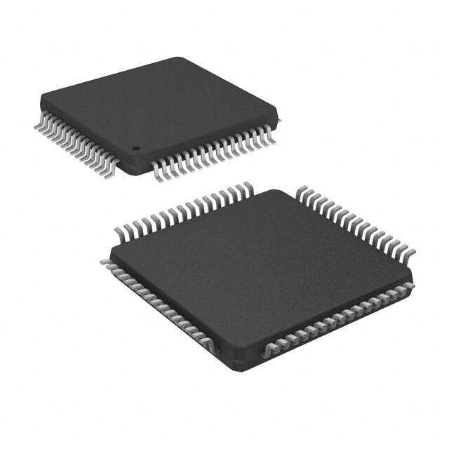
This device is available in the 64-lead TQFP package
and will operate over the industrial temperature range
of −40°C to +85°C. An evaluation board is available
to facilitate the product evaluation process
1
2
Please be aware that an important notice concerning availability, standard warranty, and use in critical applications of
Texas Instruments semiconductor products and disclaimers thereto appears at the end of this data sheet.
All trademarks are the property of their respective owners.
PRODUCTION DATA information is current as of publication date.
Products conform to specifications per the terms of the Texas
Instruments standard warranty. Production processing does not
necessarily include testing of all parameters.
Copyright © 2002–2013, Texas Instruments Incorporated
�ADC12D040
SNAS171E – JUNE 2002 – REVISED MARCH 2013
www.ti.com
These devices have limited built-in ESD protection. The leads should be shorted together or the device placed in conductive foam
during storage or handling to prevent electrostatic damage to the MOS gates.
Connection Diagram
Figure 1. 64-Lead TQFP Package
Package Number PAG
2
Submit Documentation Feedback
Copyright © 2002–2013, Texas Instruments Incorporated
Product Folder Links: ADC12D040
�ADC12D040
www.ti.com
SNAS171E – JUNE 2002 – REVISED MARCH 2013
Stage
1
Stage
2
Stage
3
Stage
n
| |
S/H
VIN A-
Stage
9
Stage
10
2
||
2
VA
Stage
11
AGND
2
||
VIN A+
| |
Block Diagram
22
Timing
Control
11-Stage Pipeline Converter
3
CLK
VD
Digital Correction
DGND
12
12
VRP A
Output
Buffers
VRM A
DA0-DA11
OEA
VRN A
VDR
INT/EXT REF
DR GND
Bandgap
Reference
VREF
VRP B
OF
12
Output
Buffers
VRM B
VRN B
DB0-DB11
OEB
12
DGND
PD
Digital Correction
VD
3
11-Stage Pipeline Converter
Timing
Control
22
Stage
2
Stage
3
Stage
n
2
| |
Stage
1
2
| |
S/H
VIN B+
||
||
2
VIN B-
Stage
9
Stage
10
Stage
11
VA
AGND
Submit Documentation Feedback
Copyright © 2002–2013, Texas Instruments Incorporated
Product Folder Links: ADC12D040
3
�ADC12D040
SNAS171E – JUNE 2002 – REVISED MARCH 2013
www.ti.com
PIN DESCRIPTIONS AND EQUIVALENT CIRCUITS
Pin No.
Symbol
Equivalent Circuit
Description
ANALOG I/O
15
2
VINA+
VINB+
Non-Inverting analog signal Inputs. With a 2.0V reference the fullscale input signal level is 2.0 VP-P on each pin of the input pair,
centered on a common VCM.
16
1
VINA−
VINB−
Inverting analog signal Input. With a 2.0V reference the full-scale
input signal level is 2.0 VP-P on each pin of the input pair, centered
on a common VCM. These (-) input pins may be connected to a
common VCM for single-ended operation, but a differential input
signal is required for best performance.
7
VREF
Reference input. This pin should be bypassed to AGND with a 0.1
µF monolithic capacitor when external reference is used. VREF is
2.0V nominal and should be between 1.0V to 2.4V.
11
INT/EXT REF
13
5
VRPA
VRPB
14
4
VRMA
VRMB
VREF select pin. With a logic low at this pin the internal 2.0V
reference is selected. With a logic high on this pin an external
reference voltage must be applied to VREF input pin 7.
These pins are high impedance reference bypass pins only. Connect
a 0.1 µF capacitor from each of these pins to AGND. DO NOT LOAD
these pins.
12
6
VRNA
VRNB
DIGITAL I/O
4
60
CLK
22
41
OEA
OEB
59
PD
21
OF
VA
Digital clock input. The range of frequencies for this input is 100 kHz
to 55 MHz (typical) with guaranteed performance at 40 MHz. The
input is sampled on the rising edge of this input.
OEA and OEB are the output enable pins that, when low, enables
their respective TRI-STATE data output pins. When either of these
pins is high, the corresponding outputs are in a high impedance
state.
PD is the Power Down input pin. When high, this input puts the
converter into the power down mode. When this pin is low, the
converter is in the active mode.
DGND
Output Format pin. A logic low on this pin causes output data to be
in offset binary format. A logic high on this pin causes the output
data to be in 2’s complement format.
Submit Documentation Feedback
Copyright © 2002–2013, Texas Instruments Incorporated
Product Folder Links: ADC12D040
�ADC12D040
www.ti.com
SNAS171E – JUNE 2002 – REVISED MARCH 2013
PIN DESCRIPTIONS AND EQUIVALENT CIRCUITS (continued)
Pin No.
Symbol
24–29
34–39
DA0–DA11
42–47
52–57
Equivalent Circuit
DB0–DB11
Description
Digital data output pins that make up the 12-bit conversion results of
their respective converters. DA0 and DB0 are the LSBs, while DA11
and DB11 are the MSBs of the output word. Output levels are
TTL/CMOS compatible.
ANALOG POWER
9, 18, 19,
62, 63
VA
3, 8, 10, 17,
20, 61, 64
AGND
Positive analog supply pins. These pins should be connected to a
quiet +5V source and bypassed to AGND with 0.1 µF monolithic
capacitors located within 1 cm of these power pins, and with a 10 µF
capacitor.
The ground return for the analog supply.
DIGITAL POWER
33, 48
VD
32, 49
DGND
30, 51
23, 31, 40,
50, 58
Positive digital supply pin. This pin should be connected to the same
quiet +5V source as is VA and be bypassed to DGND with a 0.1 µF
monolithic capacitor located within 1 cm of the power pin and with a
10 µF capacitor.
The ground return for the digital supply.
VDR
Positive digital supply pins for the ADC12D040's output drivers.
These pins should be connected to a voltage source of +2.4V to +5V
and bypassed to DR GND with a 0.1 µF monolithic capacitor. If the
supply for these pins are different from the supply used for VA and
VD, they should also be bypassed with a 10 µF tantalum capacitor.
VDR should never exceed the voltage on VD. All bypass capacitors
should be located within 1 cm of the supply pin.
DR GND
The ground return for the digital supply for the ADC12D040's output
drivers. These pins should be connected to the system digital
ground, but not be connected in close proximity to the ADC12D040's
DGND or AGND pins. See LAYOUT AND GROUNDING (Layout and
Grounding) for more details.
Submit Documentation Feedback
Copyright © 2002–2013, Texas Instruments Incorporated
Product Folder Links: ADC12D040
5
�ADC12D040
SNAS171E – JUNE 2002 – REVISED MARCH 2013
www.ti.com
Absolute Maximum Ratings (1) (2) (3)
VA, VD, VDR
6.5V
VDR
VD + 0.3V
≤ 100 mV
|VA–VD|
−0.3V to (VA or VD +0.3V)
Voltage on Any Input or Output Pin
Input Current at Any Pin (4)
±25 mA
Package Input Current (4)
±50 mA
Package Dissipation at TA = 25°C
ESD Susceptibility
(6)
See
Human Body Model
2500V
Machine Model
250V
Soldering Temperature, Infrared, 10 sec. (7)
235°C
−65°C to +150°C
Storage Temperature
(1)
(2)
(3)
(4)
(5)
(6)
(7)
(5)
All voltages are measured with respect to GND = AGND = DGND DR GND = 0V, unless otherwise specified.
Absolute Maximum Ratings indicate limits beyond which damage to the device may occur. Operating Ratings indicate conditions for
which the device is functional, but do not guarantee specific performance limits. For guaranteed specifications and test conditions, see
the Electrical Characteristics. The guaranteed specifications apply only for the test conditions listed. Some performance characteristics
may degrade when the device is not operated under the listed test conditions.
If Military/Aerospace specified devices are required, please contact the Texas Instruments Sales Office/ Distributors for availability and
specifications.
When the input voltage at any pin exceeds the power supplies (that is, VIN < AGND, or VIN > VA), the current at that pin should be
limited to 25 mA. The 50 mA maximum package input current rating limits the number of pins that can safely exceed the power supplies
with an input current of 25 mA to two.
The absolute maximum junction temperature (TJmax) for this device is 150°C. The maximum allowable power dissipation is dictated by
TJmax, the junction-to-ambient thermal resistance (θJA), and the ambient temperature, (TA), and can be calculated using the formula
PDMAX = (TJmax - TA )/θJA. The values for maximum power dissipation listed above will be reached only when the device is operated in
a severe fault condition (e.g. when input or output pins are driven beyond the power supply voltages, or the power supply polarity is
reversed). Obviously, such conditions should always be avoided.
Human body model is 100 pF capacitor discharged through a 1.5 kΩ resistor. Machine model is 220 pF discharged through 0Ω.
The 235°C reflow temperature refers to infrared reflow. For Vapor Phase Reflow (VPR), the following Conditions apply: Maintain the
temperature at the top of the package body above 183°C for a minimum 60 seconds. The temperature measured on the package body
must not exceed 220°C. Only one excursion above 183°C is allowed per reflow cycle.
Operating Ratings (1) (2)
Operating Temperature
−40°C ≤ TA ≤ +85°C
Supply Voltage (VA, VD)
+4.75V to +5.25V
Output Driver Supply (VDR)
+2.35V to VD
VREF Input
1.0V to 2.4V
−0.5V to (VD + 0.5V)
CLK, PD, OE
−0V to (VA − 0.5V)
Analog Input Pins
VREF/2 to VA − VREF
Input Common Mode Voltage (VCM)
≤100mV
|AGND–DGND|
(1)
(2)
Absolute Maximum Ratings indicate limits beyond which damage to the device may occur. Operating Ratings indicate conditions for
which the device is functional, but do not guarantee specific performance limits. For guaranteed specifications and test conditions, see
the Electrical Characteristics. The guaranteed specifications apply only for the test conditions listed. Some performance characteristics
may degrade when the device is not operated under the listed test conditions.
All voltages are measured with respect to GND = AGND = DGND DR GND = 0V, unless otherwise specified.
Package Thermal Resistance
6
Package
θJ-A
64-Lead TQFP
50°C / W
Submit Documentation Feedback
Copyright © 2002–2013, Texas Instruments Incorporated
Product Folder Links: ADC12D040
�ADC12D040
www.ti.com
SNAS171E – JUNE 2002 – REVISED MARCH 2013
Converter Electrical Characteristics
Unless otherwise specified, the following specifications apply for AGND = DGND = DR GND = 0V, VA VD +5V, VDR +3.0V, PD
= 0V, INT/EXT = VD, VREF = +2.0V,OEA, OEB = 0V, fCLK = 40 MHz, tr = tf = 3 ns, CL = 20 pF/pin. Boldface limits apply for TJ
= TMIN to TMAX: all other limits TJ = 25°C (1) (2)
Symbol
Parameter
Conditions
Typical
Limits
12
Bits (min)
±0.7
±2.0
LSB (max)
(3)
(3)
Units
(Limits)
STATIC CONVERTER CHARACTERISTICS
Resolution with No Missing Codes
INL
Integral Non Linearity (4)
DNL
Differential Non Linearity
GE
Gain Error
TC GE
Gain Error Tempco
VOFF
Offset Error (VIN+ = VIN−)
TC VOFF
Offset Error Tempco
±0.4
±1.0
LSB (max)
Positive Error
0.51
+2.8/−1.9
%FS
Negative Error
0.68
+4/−2.7
%FS
External Reference
15
ppm/ºC
Internal Reference
100
ppm/ºC
−0.1
±1.2
%FS (max)
External Reference
3
ppm/ºC
Internal Reference
3
ppm/ºC
Under Range Output Code
0
0
Over Range Output Code
4095
4095
DYNAMIC CONVERTER CHARACTERISTICS
FPBW
Full Power Bandwidth
SNR
Signal-to-Noise Ratio
SINAD
Signal-to-Noise and Distortion
100
fIN = 1 MHz, VIN = −0.5 dBFS
69
fIN = 10 MHz, VIN = −0.5 dBFS
68
fIN = 1 MHz, VIN = −0.5 dBFS
69
MHz
dB
66.5
dB (min)
dB
fIN = 10 MHz, VIN = −0.5 dBFS
68
fIN = 1 MHz, VIN = −0.5 dBFS
11.1
fIN = 10 MHz, VIN = −0.5 dBFS
10.9
fIN = 1 MHz, VIN = −0.5 dBFS
−80
fIN = 10 MHz, VIN = −0.5 dBFS
−78
fIN = 1 MHz, VIN = −0.5 dBFS
−84
fIN = 10 MHz, VIN = −0.5 dBFS
−80
fIN = 1 MHz, VIN = −0.5 dBFS
−84
fIN = 10 MHz, VIN = −0.5 dBFS
−82
fIN = 1 MHz, VIN = −0.5 dBFS
84
fIN = 10 MHz, VIN = −0.5 dBFS
80
fIN = 9.6 MHz and 10.2 MHz, each = −6.0
dBFS
−80
dBFS
Channel—Channel Offset Match
±0.02
%FS
Channel—Channel Gain Error Match
±0.05
%FS
−80
dB
ENOB
Effective Number of Bits
THD
Total Harmonic Distortion
H2
Second Harmonic
H3
Third Harmonic
SFDR
Spurious Free Dynamic Range
IMD
0 dBFS Input, Output at −3 dB
Intermodulation Distortion
65.6
dB (min)
10.6
Bits (min)
−69
dB (max)
−73
dB (max)
−69.5
dB (max)
Bits
dB
dB
dB
dB
69.5
dB (min)
INTER-CHANNEL CHARACTERISTICS
Crosstalk
(1)
(2)
(3)
(4)
10 MHz Tested Channel. 15 MHz Other
Channel
The inputs are protected as shown below. Input voltage magnitudes above VA or below GND will not damage this device, provided
current is limited, see Note 4 in the Absolute Maximum Ratings table. However, errors in the A/D conversion can occur if the input goes
above VA or below GND by more than 100 mV. As an example, if VA is 4.75V, the full-scale input voltage must be ≤4.85V to ensure
accurate conversions (see Figure 2).
To guarantee accuracy, it is required that |VA–VD| ≤ 100 mV and separate bypass capacitors are used at each power supply pin.
Typical figures are at TA = TJ = 25°C, and represent most likely parametric norms. Test limits are guaranteed to AOQL (Average
Outgoing Quality Level).
Integral Non Linearity is defined as the deviation of the analog value, expressed in LSBs, from the straight line that passes through
positive and negative full-scale.
Submit Documentation Feedback
Copyright © 2002–2013, Texas Instruments Incorporated
Product Folder Links: ADC12D040
7
�ADC12D040
SNAS171E – JUNE 2002 – REVISED MARCH 2013
www.ti.com
Converter Electrical Characteristics (continued)
Unless otherwise specified, the following specifications apply for AGND = DGND = DR GND = 0V, VA VD +5V, VDR +3.0V, PD
= 0V, INT/EXT = VD, VREF = +2.0V,OEA, OEB = 0V, fCLK = 40 MHz, tr = tf = 3 ns, CL = 20 pF/pin. Boldface limits apply for TJ
= TMIN to TMAX: all other limits TJ = 25°C(1)(2)
Symbol
Parameter
Typical
Conditions
(3)
Limits
(3)
Units
(Limits)
REFERENCE AND ANALOG INPUT CHARACTERISTICS
CIN
VIN Input Capacitance (each pin to GND)
VIN = 2.5 Vdc + 0.7 Vrms
(CLK LOW)
8
(CLK HIGH)
7
pF
pF
VREF
Input Reference Voltage (5)
2.00
RREF
Reference Input Resistance
100
VIN
(5)
Analog Input Voltage Range
1.0
V (min)
2.4
V (max)
MΩ (min)
0
V (min)
4
V (max)
Optimum performance will be obtained by keeping the reference input in the 1.8V to 2.4V range. The LM4051CIM3-ADJ (SOT23
package) is recommended for this application.
DC and Logic Electrical Characteristics
Unless otherwise specified, the following specifications apply for AGND = DGND = DR GND = 0V, VA = VD = +5V, VDR =
+3.0V, PD = 0V, INT/EXT = VD, VREF = +2.0V,OEA, OEB = 0V, fCLK = 40 MHz, tr = tf = 3 ns, CL = 20 pF/pin. Boldface limits
apply for TJ = TMIN to TMAX: all other limits TJ = 25°C (1) (2) (3)
Symbol
Parameter
Conditions
Typical
(4)
Limits
(4)
Units
(Limits)
CLK, PD, OE DIGITAL INPUT CHARACTERISTICS
VIN(1)
Logical “1” Input Voltage
VD = 5.25V
2.0
V (min)
VIN(0)
Logical “0” Input Voltage
VD = 4.75V
1.0
V (max)
IIN(1)
Logical “1” Input Current
VIN = 5.0V
10
µA
IIN(0)
Logical “0” Input Current
VIN = 0V
−10
µA
CIN
Digital Input Capacitance
5
pF
(1)
(2)
(3)
(4)
8
The inputs are protected as shown below. Input voltage magnitudes above VA or below GND will not damage this device, provided
current is limited, see Note 4 in the Absolute Maximum Ratings table. However, errors in the A/D conversion can occur if the input goes
above VA or below GND by more than 100 mV. As an example, if VA is 4.75V, the full-scale input voltage must be ≤4.85V to ensure
accurate conversions (see Figure 2).
To guarantee accuracy, it is required that |VA–VD| ≤ 100 mV and separate bypass capacitors are used at each power supply pin.
With the test condition for VREF = +2.0V (4VP-P differential input), the 12-bit LSB is 977 µV.
Typical figures are at TA = TJ = 25°C, and represent most likely parametric norms. Test limits are guaranteed to AOQL (Average
Outgoing Quality Level).
Submit Documentation Feedback
Copyright © 2002–2013, Texas Instruments Incorporated
Product Folder Links: ADC12D040
�ADC12D040
www.ti.com
SNAS171E – JUNE 2002 – REVISED MARCH 2013
DC and Logic Electrical Characteristics (continued)
Unless otherwise specified, the following specifications apply for AGND = DGND = DR GND = 0V, VA = VD = +5V, VDR =
+3.0V, PD = 0V, INT/EXT = VD, VREF = +2.0V,OEA, OEB = 0V, fCLK = 40 MHz, tr = tf = 3 ns, CL = 20 pF/pin. Boldface limits
apply for TJ = TMIN to TMAX: all other limits TJ = 25°C(1)(2)(3)
Symbol
Parameter
Limits
(4)
Units
(Limits)
VDR = 2.5V
2.3
V (min)
VDR = 3V
2.7
V (min)
0.4
V (max)
Conditions
Typical
(4)
D0–D11 DIGITAL OUTPUT CHARACTERISTICS
VOUT(1)
Logical “1” Output Voltage
IOUT = −0.5 mA
VOUT(0)
Logical “0” Output Voltage
IOUT = 1.6 mA, VDR = 3V
IOZ
TRI-STATE Output Current
+ISC
Output Short Circuit Source Current
−ISC
Output Short Circuit Sink Current
COUT
Digital Output Capacitance
VOUT = 2.5V or 5V
100
nA
VOUT = 0V
−100
nA
VOUT = 0V
−20
mA
VOUT = VDR
20
mA
5
pF
POWER SUPPLY CHARACTERISTICS
IA
Analog Supply Current
PD Pin = DGND, VREF = 2.0V
PD Pin = VDR
93
15
110
mA (max)
mA
ID
Digital Supply Current
PD Pin = DGND
PD Pin = VDR
16
0
18
mA (max)
mA
IDR
Digital Output Supply Current
PD Pin = DGND, CL = 0 pF (5)
PD Pin = VDR
10.5
0
12
mA (max)
mA
Total Power Consumption
PD Pin = DGND, CL = 0 pF (6)
PD Pin = VDR
600
75
700
mW
mW
Power Supply Rejection
Rejection of Full-Scale Error with
VA = 4.75V vs. 5.25V
56
PSRR1
(5)
(6)
dB
IDR is the current consumed by the switching of the output drivers and is primarily determined by load capacitance on the output pins,
the supply voltage, VDR, and the rate at which the outputs are switching (which is signal dependent). IDR=VDR(C0 x f0 + C1 x f1 +....C11 x
f11) where VDR is the output driver power supply voltage, Cn is total capacitance on the output pin, and fn is the average frequency at
which that pin is toggling.
Excludes IDR. See(6).
AC Electrical Characteristics
Unless otherwise specified, the following specifications apply for AGND = DGND = DR GND = 0V, VA = VD = +5V, VDR =
+3.0V, PD = 0V, INT/EXT = VD, VREF = +2.0V,OEA, OEB = 0V, fCLK = 40 MHz, tr = tf = 3 ns, CL = 20 pF/pin. Boldface limits
apply for TJ = TMIN to TMAX: all other limits TJ = 25°C (1) (2) (3) (4)
Symbol
Parameter
fCLK1
Maximum Clock Frequency
fCLK2
Minimum Clock Frequency
tCH
Conditions
Typical
(5)
Limits
(5)
Units
(Limits)
40
MHz (min)
100
kHz
Clock High Time
9
ns
tCL
Clock Low Time
9
tCONV
Conversion Latency
tOD
Data Output Delay after Rising CLK Edge VDR = 3.0V
10
tAD
Aperture Delay
1.2
ns
tAJ
Aperture Jitter
2
ps rms
tHOLD
Clock Edge to Data Transition
8
ns
(1)
(2)
(3)
(4)
(5)
ns
6
Clock Cycles
17.5
ns (max)
The inputs are protected as shown below. Input voltage magnitudes above VA or below GND will not damage this device, provided
current is limited, see Note 4 in the Absolute Maximum Ratings table. However, errors in the A/D conversion can occur if the input goes
above VA or below GND by more than 100 mV. As an example, if VA is 4.75V, the full-scale input voltage must be ≤4.85V to ensure
accurate conversions (see Figure 2).
To guarantee accuracy, it is required that |VA–VD| ≤ 100 mV and separate bypass capacitors are used at each power supply pin.
With the test condition for VREF = +2.0V (4VP-P differential input), the 12-bit LSB is 977 µV.
Timing specifications are tested at TTL logic levels, VIL = 0.4V for a falling edge and VIH = 2.4V for a rising edge.
Typical figures are at TA = TJ = 25°C, and represent most likely parametric norms. Test limits are guaranteed to AOQL (Average
Outgoing Quality Level).
Submit Documentation Feedback
Copyright © 2002–2013, Texas Instruments Incorporated
Product Folder Links: ADC12D040
9
�ADC12D040
SNAS171E – JUNE 2002 – REVISED MARCH 2013
www.ti.com
AC Electrical Characteristics (continued)
Unless otherwise specified, the following specifications apply for AGND = DGND = DR GND = 0V, VA = VD = +5V, VDR =
+3.0V, PD = 0V, INT/EXT = VD, VREF = +2.0V,OEA, OEB = 0V, fCLK = 40 MHz, tr = tf = 3 ns, CL = 20 pF/pin. Boldface limits
apply for TJ = TMIN to TMAX: all other limits TJ = 25°C(1)(2)(3)(4)
Symbol
Parameter
tDIS
Data outputs into TRI-STATE Mode
tEN
Data Outputs Active after TRI-STATE
tPD
Power Down Mode Exit Cycle
Typical
Conditions
(5)
Limits
(5)
Units
(Limits)
4
ns
4
ns
500
ns
Figure 2.
Specification Definitions
APERTURE DELAY is the time after the rising edge of the clock to when the input signal is acquired or held for
conversion.
APERTURE JITTER (APERTURE UNCERTAINTY) is the variation in aperture delay from sample to sample.
Aperture jitter manifests itself as noise in the output.
CLOCK DUTY CYCLE is the ratio of the time during one cycle that a repetitive digital waveform is high to the
total time of one period. The specification here refers to the ADC clock input signal.
COMMON MODE VOLTAGE (VCM) is the d.c. potential present at both signal inputs to the ADC.
CONVERSION LATENCY See PIPELINE DELAY.
CROSSTALK is coupling of energy from one channel into the other channel.
DIFFERENTIAL NON-LINEARITY (DNL) is the measure of the maximum deviation from the ideal step size of 1
LSB.
EFFECTIVE NUMBER OF BITS (ENOB, or EFFECTIVE BITS) is another method of specifying Signal-to-Noise
and Distortion or SINAD. ENOB is defined as (SINAD - 1.76) / 6.02 and says that the converter is equivalent to a
perfect ADC of this (ENOB) number of bits.
FULL POWER BANDWIDTH is a measure of the frequency at which the reconstructed output fundamental
drops 3 dB below its low frequency value for a full scale input.
GAIN ERROR is the deviation from the ideal slope of the transfer function. It can be calculated as:
Gain Error = Positive Full Scale Error − Negative Full-Scale Error
(1)
Gain Error can also be separated into Positive Gain Error and Negative Gain Error, which are.
PGE = Positive Full-Scale Error − Offset Error
NGE = Offset Error − Negative Full-Scale Error
(2)
(3)
GAIN ERROR MATCHING is the difference in gain errors between the two converters divided by the average
gain of the converters.
10
Submit Documentation Feedback
Copyright © 2002–2013, Texas Instruments Incorporated
Product Folder Links: ADC12D040
�ADC12D040
www.ti.com
SNAS171E – JUNE 2002 – REVISED MARCH 2013
INTEGRAL NON LINEARITY (INL) is a measure of the deviation of each individual code from a line drawn from
negative full scale (½ LSB below the first code transition) through positive full scale (½ LSB above the last code
transition). The deviation of any given code from this straight line is measured from the center of that code value.
INTERMODULATION DISTORTION (IMD) is the creation of additional spectral components as a result of two
sinusoidal frequencies being applied to the ADC input at the same time. It is defined as the ratio of the power in
the intermodulation products to the total power in the original frequencies. IMD is usually expressed in dBFS.
LSB (LEAST SIGNIFICANT BIT) is the bit that has the smallest value or weight of all bits. This value is VREF /
2n, where “n” is the ADC resolution in bits, which is 12 in the case of the ADC12D040.
MISSING CODES are those output codes that will never appear at the ADC outputs. The ADC12D040 is
guaranteed not to have any missing codes.
MSB (MOST SIGNIFICANT BIT) is the bit that has the largest value or weight. Its value is one half of full scale.
NEGATIVE FULL SCALE ERROR is the difference between the actual first code transition and its ideal value of
½ LSB above negative full scale.
OFFSET ERROR is the difference between the two input voltages (VIN+ –VIN−) required to cause a transition
from code 2047 to 2048.
OUTPUT DELAY is the time delay after the rising edge of the clock before the data update is presented at the
output pins.
OVER RANGE RECOVERY TIME is the time required after VIN goes from a specified voltage out of the normal
input range to a specified voltage within the normal input range and the converter makes a conversion with its
rated accuracy.
PIPELINE DELAY (LATENCY) is the number of clock cycles between initiation of conversion and when that data
is presented to the output driver stage. Data for any given sample is available at the output pins the Pipeline
Delay plus the Output Delay after the sample is taken. New data is available at every clock cycle, but the data
lags the conversion by the pipeline delay.
POSITIVE FULL SCALE ERROR is the difference between the actual last code transition and its ideal value of
1½ LSB below positive full scale.
POWER SUPPLY REJECTION RATIO (PSRR) is a measure of how well the ADC rejects a change in the power
supply voltage. For the ADC12D040, PSRR1 is the ratio of the change in Full-Scale Error that results from a
change in the d.c. power supply voltage, expressed in dB. PSRR2 is a measure of how well an a.c. signal riding
upon the power supply is rejected at the output.
SIGNAL TO NOISE RATIO (SNR) is the ratio, expressed in dB, of the rms value of the input signal to the rms
value of the sum of all other spectral components below one-half the sampling frequency, not including
harmonics or d.c.
SIGNAL TO NOISE PLUS DISTORTION (S/N+D or SINAD) Is the ratio, expressed in dB, of the rms value of the
input signal to the rms value of all of the other spectral components below half the clock frequency, including
harmonics but excluding d.c.
SPURIOUS FREE DYNAMIC RANGE (SFDR) is the difference, expressed in dB, between the rms values of the
input signal and the peak spurious signal, where a spurious signal is any signal present in the output spectrum
that is not present at the input.
Submit Documentation Feedback
Copyright © 2002–2013, Texas Instruments Incorporated
Product Folder Links: ADC12D040
11
�ADC12D040
SNAS171E – JUNE 2002 – REVISED MARCH 2013
www.ti.com
TOTAL HARMONIC DISTORTION (THD) is the ratio, expressed in dB, of the rms total of the first seven
harmonic levels at the output to the level of the fundamental at the output. THD is calculated as
where
•
f1 is the RMS power of the fundamental (output) frequency and f2 through f10 are the RMS power of the first 9
harmonic frequencies in the output spectrum.
(4)
– Second Harmonic Distortion (2ND HARM) is the difference expressed in dB, between the RMS power in the
input frequency at the output and the power in its 2nd harmonic level at the output.
– Third Harmonic Distortion (3RD HARM) is the difference, expressed in dB, between the RMS power in the
input frequency at the output and the power in its 3rd harmonic level at the output.
Timing Diagram
Figure 3. Output Timing
Transfer Characteristic
Figure 4. Transfer Characteristic
12
Submit Documentation Feedback
Copyright © 2002–2013, Texas Instruments Incorporated
Product Folder Links: ADC12D040
�ADC12D040
www.ti.com
SNAS171E – JUNE 2002 – REVISED MARCH 2013
Typical Performance Characteristics
VA = VD = 5V, VDR = 3V, fCLK = 40 MHz, fIN = 10 MHz unless otherwise stated
DNL
INL
0.5
1
0.4
0.3
0.5
0.2
BITS
BITS
0.1
0
0
-0.1
-0.2
-0.5
-0.3
-0.4
-0.5
-1
0
1024
2048
3072
4096
0
1024
2048
3072
OUTPUT CODE
OUTPUT CODE
Figure 5.
Figure 6.
INL & DNL
vs.
Supply Voltage
DNL & INL
vs.
Clock Frequency
1
4096
2
0.8
1.5
+INL
0.6
1
0.4
+INL
+DNL
0.5
0
LSB
LSBs
0.2
-0.2
-DNL
+DNL
0
-DNL
-0.5
-0.4
-INL
-1
-0.6
-INL
-0.8
-1.5
-1
4.5/ 4.75/ 5.0/
4.5 4.75 2.5
5.0/ 5.0/
3.0 4.0
VA/V_DR
-2
5.0/ 5.25/ 5.5/
5.0 5.25 5.5
5
20
40
50
55
CLOCK FREQUENCY (MHz)
Figure 7.
Figure 8.
DNL & INL
vs.
Clock Duty Cycle
DNL & INL
vs.
Reference Voltage
3
1.5
2
1
+INL
0.5
+INL
LSB
LSB
1
+DNL
0
-DNL
-1
+DNL
0
-DNL
-0.5
-INL
-INL
-2
-1
-3
35
40
45
50
55
60
65
-1.5
CLOCK DUTY CYCLE
0.8
1
1.2 1.4 1.6
2
2.4 2.6 2.8
3
REFERENCE VOLTAGE, V
Figure 9.
Figure 10.
Submit Documentation Feedback
Copyright © 2002–2013, Texas Instruments Incorporated
Product Folder Links: ADC12D040
13
�ADC12D040
SNAS171E – JUNE 2002 – REVISED MARCH 2013
www.ti.com
Typical Performance Characteristics (continued)
VA = VD = 5V, VDR = 3V, fCLK = 40 MHz, fIN = 10 MHz unless otherwise stated
INL & DNL
vs. Temperature
SNR, SINAD, SFDR
vs. Supply Voltage
1
85
SFDR
0.8
+INL
0.6
80
0.4
+DNL
75
dB
LSB
0.2
0
-0.2
70
-DNL
SNR
-0.4
SINAD
-0.6
65
-INL
-0.8
-1
-40
25
60
4.5/ 4.75/ 5.0/
4.5 4.75 2.5
85
TEMPERATURE (°C)
5.0/
3.0
5.0/ 5.25/ 5.5/
5.0 5.25 5.5
5.0/
4.0
VA/VDR, Volts
Figure 11.
Figure 12.
SNR, SINAD, SFDR
vs.
Clock Frequency
SNR, SINAD, SFDR
vs.
Clock Duty Cycle
90
85
SFDR
85
80
SFDR
80
dB
dB
75
75
70
70
SNR
SNR
SINAD
65
SINAD
65
60
10
60
20
40
45
50
55
35
60
40
45
50
55
60
65
CLOCK DUTY CYCLE, %
CLOCK FREQUENCY, MHz
Figure 13.
Figure 14.
SNR, SINAD, SFDR
vs.
Input Frequency
SNR, SINAD, SFDR
vs.
Reference Voltage
90
85
80
85
SFDR
SFDR
75
65
SINAD
dB
SNR
dB
80
70
70
60
SNR
SINAD
65
55
50
60
0
10
20
30
40
INPUT FREQUENCY (MHZ)
0.8
1
1.2 1.4 1.6
2
2.4 2.6 2.8
3
REFERENCE VOLTAGE, V
Figure 15.
14
75
Figure 16.
Submit Documentation Feedback
Copyright © 2002–2013, Texas Instruments Incorporated
Product Folder Links: ADC12D040
�ADC12D040
www.ti.com
SNAS171E – JUNE 2002 – REVISED MARCH 2013
Typical Performance Characteristics (continued)
VA = VD = 5V, VDR = 3V, fCLK = 40 MHz, fIN = 10 MHz unless otherwise stated
SNR, SINAD, SFDR
vs. Temperature
Distortion
vs.Supply Voltage
-70
-72
-74
-76
THD
dB
-78
-80
3rd Harmonic
-82
-84
-86
2nd Harmonic
-88
-90
4.5/ 4.75/ 5.0/
4.5 4.75 2.5
5.0/ 5.0/ 5.0/ 5.25/ 5.5/
3.0 4.0 5.0 5.25 5.5
VA/VDR, Volts
Figure 17.
Figure 18.
Distortion vs.
Clock Frequency
Distortion
vs.
Clock Duty Cycle
-68
-60
-70
-65
-72
-74
dB
dB
-70
-75
THD
-76
-78
THD
-80
HAR2
-80
HAR3
-82
-85
HAR2
-90
10
HAR3
-84
-86
20
40
45
50
55
35
60
40
45
50
55
60
65
CLOCK DUTY CYCLE
FCLK, MHz
Figure 19.
Figure 20.
Distortion
vs.
Input Frequency
Distortion
vs.
Reference Voltage
-40
-60
-45
-65
-50
-55
-70
-75
THD
-65
dB
dB
-60
-70
-80
HAR3
-75
THD
-85
-80
HAR2
3rd Harmonic
-85
-90
2nd Harmonic
-90
0
10
20
30
40
INPUT FREQUENCY, MHz
-95
0.8
1
1.2 1.4 1.6
2
2.4 2.6 2.8
3
VREF, V
Figure 21.
Figure 22.
Submit Documentation Feedback
Copyright © 2002–2013, Texas Instruments Incorporated
Product Folder Links: ADC12D040
15
�ADC12D040
SNAS171E – JUNE 2002 – REVISED MARCH 2013
www.ti.com
Typical Performance Characteristics (continued)
VA = VD = 5V, VDR = 3V, fCLK = 40 MHz, fIN = 10 MHz unless otherwise stated
Distortion
vs.Temperature
Power Consumption
vs.Reference Voltage
800
750
700
mW
650
600
550
500
450
400
0.8
1
1.2 1.4 1.6
2
2.4 2.6 2.8 3
VREF, V
750
Figure 23.
Figure 24.
Power Consumption
vs.
Temperature
Spectral Response @ Fin = 9.95 MHz,
FCLK = 40 MHz
45 MSPS
40 MSPS
50 MSPS
700
60 MSPS
55 MSPS
600
dB
POWER mW
650
550
500
10
0
-10
-20
-30
-40
-50
-60
-70
-80
-90
-100
-110
-120
SINAD: 68.569
SNR: 68.894
THD: -79.989
SFDR: 81.384
ENOB: 11.098
Fundamental
9.95 MHz
H3
SFDR
10.15 MHz
H5
9.75 MHz
H4
200.195 kHz
H7
10.35 MHz
H2
19.9 MHz
H6
19.7 MHz
450
20 MSPS
30 MSPS
400
-40
10 MSPS
5 MSPS
25
0
85
2
4
8 10 12 14 16 18 20
FREQUENCY, MHz
TEMPERATURE, °C
Figure 25.
Figure 26.
IMD Response Fin = 9.6 MHz, 10.2 MHz,
FCLK = 40 MHz
Crosstalk Response Fin = 9.95 MHz,
FCROSSTALK = 15 MHz, FCLK = 40 MHz
10
0
-10
-20
-30
-40
-50
-60
-70
-80
-90
-100
-110
-120
9.6 MHz
10.2 MHz
IMD -85.837
dB
dB
6
19.8 MHz
600.586 kHz
0
2
4
6
8 10 12 14 16 18 20
10
0
-10
-20
-30
-40
-50
-60
-70
-80
-90
-100
-110
-120
Fundamental
9.95 MHz
HH 33
SFDR
SFDR
10.15MHz
MHz
10.15
H5
HH77
9.75 MHz
10.35
10.35MHz
MHz
H4
200.195 kHz
0
2
4
6
SINAD:68.452
68.452
SINAD:
SNR:68.83
68.83
SNR:
THD:-79.241
-79.241
THD:
SFDR:80.201
80.201
SFDR:
ENOB:11.078
11.078
ENOB:
H2
19.9 MHz
H6
19.7 MHz
8 10 12 14 16 18 20
FREQUENCY, MHz
FREQUENCY, MHz
Figure 27.
16
Figure 28.
Submit Documentation Feedback
Copyright © 2002–2013, Texas Instruments Incorporated
Product Folder Links: ADC12D040
�ADC12D040
www.ti.com
SNAS171E – JUNE 2002 – REVISED MARCH 2013
FUNCTIONAL DESCRIPTION
Operating on a single +5V supply, the ADC12D040 uses a pipeline architecture and has error correction circuitry
to help ensure maximum performance. The differential analog input signal is digitized to 12 bits and the reference
input is buffered to ease the task of driving that pin.
The output word rate is the same as the clock frequency, which can be between 100 ksps (typical) and 40 Msps
with fully specified performance at 40 Msps. The analog input voltage for both channels is acquired at the rising
edge of the clock and the digital data for a given sample is delayed by the pipeline for 6 clock cycles. A choice of
Offset Binary or Two's Complement output format is selected with the OF pin.
A logic high on the power down (PD) pin reduces the converter power consumption to 75 mW.
APPLICATIONS INFORMATION
OPERATING CONDITIONS
We recommend that the following conditions be observed for operation of the ADC12D040:
4.75V ≤ VA ≤ 5.25V
VD = VA
2.35V ≤ VDR ≤ VD
VREF/2 ≤ VCM ≤ VA - VREF
100 kHz ≤ fCLK ≤ 40 MHz
1.0V ≤ VREF ≤ 2.4V
Analog Inputs
The ADC12D040 has two analog signal inputs, VIN+ and VIN−. These two pins form a differential input pair. There
is one reference input pin, VREF.
The analog input circuitry contains an input boost circuit that provides improved linearity over a wide range of
analog input voltages. To prevent an on-chip over voltage condition that could impair device reliability, the input
signal should never exceed the voltage described as
VA - VREF/2.
(5)
Reference Pins
The ADC12D040 is designed to operate with a 2.0V reference, but performs well with reference voltages in the
range of 1.0V to 2.4V. Lower reference voltages will decrease the signal-to-noise ratio (SNR) of the ADC12D040.
Increasing the reference voltage (and the input signal swing) beyond 2.4V may degrade THD for a full-scale input
especially at higher input frequencies. It is important that all grounds associated with the reference voltage and
the input signal make connection to the analog ground plane at a single point in that plane to minimize the
effects of noise currents in the ground path.
The ADC12040 will perform well with reference voltages up to 2.4V for full-scale input frequencies up to 10 MHz.
However, more headroom is needed as the input frequency increases, so the maximum reference voltage (and
input swing) will decrease for higher full-scale input frequencies.
The six Reference Bypass Pins (VRPA, VRMA, VRNA, VRPB, VRMB and VRNB) are made available for bypass
purposes. These pins should each be bypassed to ground with a 0.1 µF capacitor. Smaller capacitor values will
allow faster recovery from the power down mode, but may result in degraded noise performance. DO NOT LOAD
these pins. Loading any of these pins may result in performance degradation.
The nominal voltages for the reference bypass pins are as follows:
VRMA = VRMB = VA / 2
VRPA = VRPB = VRM + VREF / 2
VRNA = VRNB = VRM − VREF / 2
Submit Documentation Feedback
Copyright © 2002–2013, Texas Instruments Incorporated
Product Folder Links: ADC12D040
17
�ADC12D040
SNAS171E – JUNE 2002 – REVISED MARCH 2013
www.ti.com
The VRN pins may be used as a common mode voltage source (VCM) for the analog input pins as long as no d.c.
current is drawn from it. However, because the voltages at these pins are half that of the VA supply pin, using
these pins for a common mode source will result in reduced input headroom (the difference between the VA
supply voltage and the peak signal voltage at either analog input) and the possibility of reduced THD and SFDR
performance. For this reason, it is recommended that VA always exceed VREF by at least 2 Volts. For high input
frequencies it may be necessary to increase this headroom to maintain THD and SFDR performance.
Signal Inputs
The signal inputs are VIN+ and VIN−. The input signal, VIN, is defined as
VIN = (VIN+) – (VIN−)
(6)
Figure 29 shows the expected input signal range.
Note that the common mode input voltage range is 1V to 3V with a nominal value of VA/2. The input signals
should remain between ground and 4V.
The Peaks of the individual input signals (VIN+ and VIN−) should each never exceed the voltage described as
VIN+, VIN− = (VREF / 2 + VCM) ≤ 4V (differential)
(7)
to maintain THD and SINAD performance.
Figure 29. Expected Input Signal Range
The ADC12D040 performs best with a differential input with each input centered around a common VCM. The
peak-to-peak voltage swing at both VIN+ and VIN− should not exceed the value of the reference voltage or the
output data will be clipped.
The two input signals should be exactly 180° out of phase from each other and of the same amplitude. For single
frequency inputs, angular errors result in a reduction of the effective full scale input. For a complex waveform,
however, angular errors will result in distortion.
For single frequency sine waves with angular errors of less than 45° (π/4) between the two inputs, the full scale
error in LSB can be described as approximately
EFS = 2(n-1) * ( 1 - cos (dev) ) = 2048 * ( 1 - cos (dev) )
(8)
Where dev is the angular difference between the two signals having a 180° relative phase relationship to each
other (see Figure 30). Drive the analog inputs with a source impedance less than 100Ω.
18
Submit Documentation Feedback
Copyright © 2002–2013, Texas Instruments Incorporated
Product Folder Links: ADC12D040
�ADC12D040
www.ti.com
SNAS171E – JUNE 2002 – REVISED MARCH 2013
Angular Errors Between the Two Input Signals Will Reduce the Output Level or Cause Distortion
Figure 30. Angular Errors Between Two Input Signals
Table 1. Input to Output Relationship – Differential Input
VIN+
VIN−
Binary Output
2’s Complement Output
VCM − VREF/2
VCM + VREF/2
0000 0000 0000
1000 0000 0000
VCM − VREF/4
VCM + VREF/4
0100 0000 0000
1100 0000 0000
VCM
VCM
1000 0000 0000
0000 0000 0000
VCM + VREF/4
VCM − VREF/4
1100 0000 0000
0100 0000 0000
VCM + VREF/2
VCM − VREF/2
1111 1111 1111
0111 1111 1111
Table 2. Input to Output Relationship – Single-Ended Input
VIN
VIN−
Binary Output
2’s Complement Output
VCM − VREF
VCM
0000 0000 0000
1000 0000 0000
VCM − VREF/2
VCM
0100 0000 0000
1100 0000 0000
VCM
VCM
1000 0000 0000
0000 0000 0000
VCM + VREF/2
VCM
1100 0000 0000
0100 0000 0000
VCM + VREF
VCM
1111 1111 1111
0111 1111 1111
+
Single-Ended Operation
Single-ended performance is lower than with differential input signals. For this reason, single-ended operation is
not recommended. However, if single ended-operation is required and the resulting performance degradation is
acceptable, one of the analog inputs should be connected to the d.c. mid point voltage of the driven input. The
peak-to-peak differential input signal should be twice the reference voltage to maximize SNR and SINAD
performance (Figure 29b).
For example, set VREF to 1.0V, bias VIN− to 2.5V and drive VIN+ with a signal range of 1.5V to 3.5V.
Because very large input signal swings can degrade distortion performance, better performance with a singleended input can be obtained by reducing the reference voltage when maintaining a full-range output. Table 1 and
Table 2 indicate the input to output relationship of the ADC12D040.
Driving the Analog Input
The VIN+ and the VIN− inputs of the ADC12D040 consist of an analog switch followed by a switched-capacitor
amplifier. The capacitance seen at the analog input pins changes with the clock level, appearing as 8 pF when
the clock is low, and 7 pF when the clock is high.
As the internal sampling switch opens and closes, current pulses occur at the analog input pins, resulting in
voltage spikes at the signal input pins. As a driving amplifier attempts to counteract these voltage spikes, a
damped oscillation may appear at the ADC analog inputs. The best amplifiers for driving the ADC12D040 input
pins must be able to react to these spikes and settle before the switch opens and another sample is taken. The
LMH6702 LMH6628 and the LMH6622, LMH6655 are good amplifiers for driving the ADC12D040.
Submit Documentation Feedback
Copyright © 2002–2013, Texas Instruments Incorporated
Product Folder Links: ADC12D040
19
�ADC12D040
SNAS171E – JUNE 2002 – REVISED MARCH 2013
www.ti.com
To help isolate the pulses at the ADC input from the amplifier output, use RCs at the inputs, as can be seen in
Figure 31 and Figure 32. These components should be placed close to the ADC inputs because the input pins of
the ADC is the most sensitive part of the system and this is the last opportunity to filter that input.
For Nyquist applications the RC pole should be at the ADC sample rate. The ADC input capacitance in the
sample mode should be considered when setting the RC pole. Setting the pole in this manner will provide best
SNR performance.
To obtain best SINAD and ENOB performance, reduce the RC time constant until SNR and THD are numerically
equal to each other. To obtain best distortion and SFDR performance, eliminate the RC altogether.
For undersampling applications, RC pole should be set at about 1.5 to 2 times the maximum input frequency to
maintain a linear delay response.
Note that the ADC12DL040 is not designed to operate with single-ended inputs. However, doing so is possible if
the degraded performance is acceptable. See Single-Ended Operation
Figure 31 shows a narrow band application with a transformer used to convert single-ended input signals to
differential. Figure 32 shows the use of a fully differential amplifier for single-ended to differential conversion.
Figure 31. Application Circuit using Transformer or Differential Op-Amp Drive Circuit
20
Submit Documentation Feedback
Copyright © 2002–2013, Texas Instruments Incorporated
Product Folder Links: ADC12D040
�ADC12D040
www.ti.com
SNAS171E – JUNE 2002 – REVISED MARCH 2013
511, 1%
51
255, 1%
50:
SIGNAL
INPUT
To ADC
VIN68 pF
+
49.9,
1%
Amplifier:
LMH6650
280, 1%
-
68 pF
511, 1%
51
To ADC
VIN+
Figure 32. Differential Drive Circuit using a fully differential amplifier.
Input Common Mode Voltage
The input common mode voltage, VCM, should be of a value such that the peak excursions of the analog signal
does not go more negative than ground or more positive than 1.0 Volts below the VA supply voltage. The nominal
VCM should generally be about VREF/2. VRBA and VRBB can be used as VCM sources as long as no d.c. current is
drawn from these pins.
DIGITAL INPUTS
Digital TTL/CMOS compatible inputs consist of CLK, OEA, OEB, OF, INT/EXT REF, and PD.
CLK
The CLK signal controls the timing of the sampling process. Drive the clock input with a stable, low jitter clock
signal in the range of 100 kHz to 55 MHz with rise and fall times of less than 3ns. The trace carrying the clock
signal should be as short as possible and should not cross any other signal line, analog or digital, not even at
90°.
If the CLK is interrupted, or its frequency too low, the charge on internal capacitors can dissipate to the point
where the accuracy of the output data will degrade. This is what limits the lowest sample
The ADC clock line should be considered to be a transmission line and be series terminated at the source end to
match the source impedance with the characteristic impedance of the clock line. It generally is not necessary to
terminate the far (ADC) end of the clock line, but if a single clock source is driving more than one device (a
condition that is generally not recommended), far end termination may be needed. Far end termination is a series
RC with the resistor being the same as the characteristic impedance of the clock line. The capacitor should have
a minimum value of
(9)
where tPD is the propagation time in ns/unit length, "L" is the length of the line and ZO is the characteristic
impedance of the line. The units of tPD and "L" should be consistent with each other. The typical board of FR-4
material has a tPD of about 150 ps/inch, or about 60 ps/cm.
The far end termination should be near but beyond the ADC clock pin as seen from the clock source.
The duty cycle of the clock signal can affect the performance of any A/D Converter. Because achieving a precise
duty cycle is difficult, the ADC12040 is designed to maintain performance over a range of duty cycles. While it is
specified and performance is guaranteed with a 50% clock duty cycle, performance is typically maintained over a
clock duty cycle range of 40% to 60%.
Take care to maintain a constant clock line impedance throughout the length of the line. Refer to Application
Note AN-905 (SNLA035) for information on setting characteristic impedance.
OEA, OEB
The OEA and OEB pin, when high, put the output pins of their respective converters into a high impedance state.
When either of these pins is low the corresponding outputs are in the active state. The ADC12D040 will continue
to convert whether these pins are high or low, but the output can not be read while the pin is high.
Submit Documentation Feedback
Copyright © 2002–2013, Texas Instruments Incorporated
Product Folder Links: ADC12D040
21
�ADC12D040
SNAS171E – JUNE 2002 – REVISED MARCH 2013
www.ti.com
Since ADC noise increases with increased output capacitance at the digital output pins, do not use the TRISTATE outputs of the ADC12L066 to drive a bus. Rather, each output pin should be located close to and drive a
single digital input pin. To further reduce ADC noise, a 100 Ω resistor in series with each ADC digital output pin,
located close to their respective pins, should be added to the circuit.
The PD Pin
The PD pin, when high, holds the ADC12D040 in a power-down mode to conserve power when the converter is
not being used. The power consumption in this state is 75 mW with a 40 MHz clock and 40mW if the clock is
stopped when PD is high. The output data pins are undefined in the power down mode and the data in the
pipeline is corrupted while in the power down mode.
The Power Down Mode Exit Cycle time is determined by the value of the capacitors on pins 4, 5, 6, 12, 13 and
14. These capacitors loose their charge in the Power Down mode and must be recharged by on-chip circuitry
before conversions can be accurate. Smaller capacitor values allow faster recovery from the power down mode,
but can result in a reduction in SNR, SINAD and ENOB performance.
The OF Pin
The output data format is offset binary when the OF pin is at a logic low or 2’s complement when the OF pin is at
a logic high. While the sense of this pin may be changed "on the fly," doing this is not recommended as the
output data could be erroneous for a few clock cycles after this change is made.
The INT/EXT REF Pin
The INT/EXT REF pin determines whether the internal reference or an external reference voltage is used. With
this pin at a logic low, the internal 2.0V reference is in use. With this pin at a logic high an external reference
must be applied to the VREF pin, which should then be bypassed to ground. There is no need to bypass the VREF
pin when the internal reference is used. There is no access to the internal reference voltage, but its value is
approximately equal to VRP − VRN. See Reference Pins
DATA OUTPUT PINS
The ADC12D040 has 24 TTL/CMOS compatible Data Output pins. Valid data is present at these outputs while
the OE and PD pins are low. While the tOD time provides information about output timing, tOD will change with a
change of clock frequency. At the rated 40 MHz clock rate, the data transition is about 6 to 10 ns after the rise of
the clock and about 4 to 10 ns before the fall of the clock (depending upon VDR), so either clock edge may be
used to capture data, depending upon the data setup time of the circuit accepting the data. Also, circuit board
layout will affect relative delays of the clock and data, so it is important to consider these relative delays when
designing the digital interface. At sample frequencies below 40 MHz, there is a longer time between data
transition and the fall of the clock, so that the falling edge of the clock is generally the best edge to use for output
data capture at low sample rates.
Be very careful when driving a high capacitance bus. The more capacitance the output drivers must charge for
each conversion, the more instantaneous digital current flows through VDR and DR GND. These large charging
current spikes can cause on-chip ground noise and couple into the analog circuitry, degrading dynamic
performance. Adequate bypassing, limiting output capacitance and careful attention to the ground plane will
reduce this problem. Additionally, bus capacitance beyond the specified 20 pF/pin will cause tOD to increase,
making it difficult to properly latch the ADC output data. The result could be an apparent reduction in dynamic
performance.
To minimize noise due to output switching, minimize the load currents at the digital outputs. This can be done by
connecting buffers (74AC541, for example) between the ADC outputs and any other circuitry. Only one driven
input should be connected to each output pin. Additionally, inserting series resistors of about 100Ω at the digital
outputs, close to the ADC pins, will isolate the outputs from trace and other circuit capacitances and limit the
output currents, which could otherwise result in performance degradation. See Figure 31.
Note that, although the ADC12D040 has Tri-State outputs, these outputs should not be used to drive a bus and
the charging and discharging of large capacitances can degrade SNR performance. Each output pin should drive
only one pin of a receiving device and the interconnecting lines should be as short as practical.
22
Submit Documentation Feedback
Copyright © 2002–2013, Texas Instruments Incorporated
Product Folder Links: ADC12D040
�ADC12D040
www.ti.com
SNAS171E – JUNE 2002 – REVISED MARCH 2013
POWER SUPPLY CONSIDERATIONS
The power supply pins should be bypassed with a 10 µF capacitor and with a 0.1 µF ceramic chip capacitor
within a centimeter of each power pin. Leadless chip capacitors are preferred because they have low series
inductance.
As is the case with all high-speed converters, the ADC12D040 is sensitive to power supply noise. Accordingly,
the noise on the analog supply pin should be kept below 100 mVP-P.
No pin should ever have a voltage on it that is in excess of the supply voltages, not even on a transient basis. Be
especially careful of this during turn on and turn off of power.
The VDR pin provides power for the output drivers and may be operated from a supply in the range of 2.35V to
VD (nominal 5V). This can simplify interfacing to low voltage devices and systems. Note, however, that tOD
increases with reduced VDR. DO NOT operate the VDR pin at a voltage higher than VD.
LAYOUT AND GROUNDING
Proper grounding and proper routing of all signals are essential to ensure accurate conversion. Maintaining
separate analog and digital areas of the board, with the ADC12D040 between these areas, is required to achieve
specified performance.
The ground return for the data outputs (DR GND) carries the ground current for the output drivers. The output
current can exhibit high transients that could add noise to the conversion process. To prevent this from
happening, the DR GND pins should NOT be connected to system ground in close proximity to any of the
ADC12D040's other ground pins.
Capacitive coupling between the typically noisy digital circuitry and the sensitive analog circuitry can lead to poor
performance. The solution is to keep the analog circuitry separated from the digital circuitry, and to keep the
clock line as short as possible.
The effects of the noise generated from the ADC output switching can be minimized through the use of 100Ω
resistors in series with each data output line. Locate these resistors as close to the ADC output pins as possible.
Submit Documentation Feedback
Copyright © 2002–2013, Texas Instruments Incorporated
Product Folder Links: ADC12D040
23
�ADC12D040
SNAS171E – JUNE 2002 – REVISED MARCH 2013
www.ti.com
Figure 33. Example of a Suitable Layout
Since digital switching transients are composed largely of high frequency components, total ground plane copper
weight will have little effect upon the logic-generated noise. This is because of the skin effect. Total surface area
is more important than is total ground plane volume.
Generally, analog and digital lines should cross each other at 90° to avoid crosstalk. To maximize accuracy in
high speed, high resolution systems, however, avoid crossing analog and digital lines altogether. It is important to
keep clock lines as short as possible and isolated from ALL other lines, including other digital lines. Even the
generally accepted 90° crossing should be avoided with the clock line as even a little coupling can cause
problems at high frequencies. This is because other lines can introduce jitter into the clock line, which can lead to
degradation of SNR. Also, the high speed clock can introduce noise into the analog chain.
Best performance at high frequencies and at high resolution is obtained with a straight signal path. That is, the
signal path through all components should form a straight line wherever possible.
Be especially careful with the layout of inductors. Mutual inductance can change the characteristics of the circuit
in which they are used. Inductors should not be placed side by side, even with just a small part of their bodies
beside each other.
The analog input should be isolated from noisy signal traces to avoid coupling of spurious signals into the input.
Any external component (e.g., a filter capacitor) connected between the converter's input pins and ground or to
the reference input pin and ground should be connected to a very clean point in the analog ground plane.
Figure 33 gives an example of a suitable layout. All analog circuitry (input amplifiers, filters, reference
components, etc.) should be placed in the analog area of the board. All digital circuitry and I/O lines should be
placed in the digital area of the board. The ADC12DL040 should be between these two areas. Furthermore, all
components in the reference circuitry and the input signal chain that are connected to ground should be
connected together with short traces and enter the analog ground plane at a single, quiet point. All ground
connections should have a low inductance path to ground.
24
Submit Documentation Feedback
Copyright © 2002–2013, Texas Instruments Incorporated
Product Folder Links: ADC12D040
�ADC12D040
www.ti.com
SNAS171E – JUNE 2002 – REVISED MARCH 2013
DYNAMIC PERFORMANCE
To achieve the best dynamic performance, the clock source driving the CLK input must be free of jitter. Isolate
the ADC clock from any digital circuitry with buffers, as with the clock tree shown in Figure 34. The gates used in
the clock tree must be capable of operating at frequencies much higher than those used if added jitter is to be
prevented.
Best performance will be obtained with a differential input drive, compared with a single-ended drive, as
discussed in Single-Ended Operation and Driving the Analog Input.
As mentioned in LAYOUT AND GROUNDING, it is good practice to keep the ADC clock line as short as possible
and to keep it well away from any other signals. Other signals can introduce jitter into the clock signal, which can
lead to reduced SNR performance, and the clock can introduce noise into other lines. Even lines with 90°
crossings have capacitive coupling, so try to avoid even these 90° crossings of the clock line.
Figure 34. Isolating the ADC Clock from other Circuitry with a Clock Tree
COMMON APPLICATION PITFALLS
Driving the inputs (analog or digital) beyond the power supply rails. For proper operation, all inputs should
not go more than 100 mV beyond the supply rails (more than 100 mV below the ground pins or 100 mV above
the supply pins). Exceeding these limits on even a transient basis may cause faulty or erratic operation. It is not
uncommon for high speed digital components (e.g., 74F devices) to exhibit overshoot or undershoot that goes
above the power supply or below ground. A resistor of about 47Ω to 100Ω in series with any offending digital
input, close to the signal source, will eliminate the problem.
Do not allow input voltages to exceed the supply voltage, even on a transient basis. Not even during power up or
power down.
Be careful not to overdrive the inputs of the ADC12D040 with a device that is powered from supplies outside the
range of the ADC12D040 supply. Such practice may lead to conversion inaccuracies and even to device
damage.
Attempting to drive a high capacitance digital data bus. The more capacitance the output drivers must
charge for each conversion, the more instantaneous digital current flows through VDR and DR GND. These large
charging current spikes can couple into the analog circuitry, degrading dynamic performance. Adequate
bypassing and maintaining separate analog and digital areas on the pc board will reduce this problem.
Additionally, bus capacitance beyond the specified 20 pF/pin will cause tOD to increase, making it difficult to
properly latch the ADC output data. The result could, again, be an apparent reduction in dynamic performance.
The digital data outputs should be buffered (with 74AC541, for example). Dynamic performance can also be
improved by adding series resistors at each digital output, close to the ADC12D040, which reduces the energy
coupled back into the converter output pins by limiting the output current. A reasonable value for these resistors
is 100Ω.
Using an inadequate amplifier to drive the analog input. As explained in Signal Inputs, the capacitance seen
at the input alternates between 8 pF and 7 pF, depending upon the phase of the clock. This dynamic load is
more difficult to drive than is a fixed capacitance.
Submit Documentation Feedback
Copyright © 2002–2013, Texas Instruments Incorporated
Product Folder Links: ADC12D040
25
�ADC12D040
SNAS171E – JUNE 2002 – REVISED MARCH 2013
www.ti.com
If the amplifier exhibits overshoot, ringing, or any evidence of instability, even at a very low level, it will degrade
performance. A small series resistor at each amplifier output and a capacitor across the analog inputs (as shown
in Figure 32) will improve performance. The LMH6702 and the LMH6628 have been successfully used to drive
the analog inputs of the ADC12D040.
Also, it is important that the signals at the two inputs have exactly the same amplitude and be exactly 180º out of
phase with each other. Board layout, especially equality of the length of the two traces to the input pins, will
affect the effective phase between these two signals. Remember that an operational amplifier operated in the
non-inverting configuration will exhibit more time delay than will the same device operating in the inverting
configuration.
Operating with the reference pins outside of the specified range. As mentioned in Reference Pins, VREF
should be in the range of
1.0V ≤ VREF ≤ 2.4V
(10)
Operating outside of these limits could lead to performance degradation.
Using a clock source with excessive jitter, using excessively long clock signal trace, or having other
signals coupled to the clock signal trace. This will cause the sampling interval to vary, causing excessive
output noise and a reduction in SNR and SINAD performance.
26
Submit Documentation Feedback
Copyright © 2002–2013, Texas Instruments Incorporated
Product Folder Links: ADC12D040
�ADC12D040
www.ti.com
SNAS171E – JUNE 2002 – REVISED MARCH 2013
REVISION HISTORY
Changes from Revision D (March 2013) to Revision E
•
Page
Changed layout of National Data Sheet to TI format .......................................................................................................... 26
Submit Documentation Feedback
Copyright © 2002–2013, Texas Instruments Incorporated
Product Folder Links: ADC12D040
27
�PACKAGE OPTION ADDENDUM
www.ti.com
10-Dec-2020
PACKAGING INFORMATION
Orderable Device
Status
(1)
Package Type Package Pins Package
Drawing
Qty
Eco Plan
(2)
Lead finish/
Ball material
MSL Peak Temp
Op Temp (°C)
(3)
Device Marking
(4/5)
(6)
ADC12D040CIVS/NOPB
ACTIVE
TQFP
PAG
64
160
RoHS & Green
SN
Level-3-260C-168 HR
-40 to 85
ADC12D040
CIVS
(1)
The marketing status values are defined as follows:
ACTIVE: Product device recommended for new designs.
LIFEBUY: TI has announced that the device will be discontinued, and a lifetime-buy period is in effect.
NRND: Not recommended for new designs. Device is in production to support existing customers, but TI does not recommend using this part in a new design.
PREVIEW: Device has been announced but is not in production. Samples may or may not be available.
OBSOLETE: TI has discontinued the production of the device.
(2)
RoHS: TI defines "RoHS" to mean semiconductor products that are compliant with the current EU RoHS requirements for all 10 RoHS substances, including the requirement that RoHS substance
do not exceed 0.1% by weight in homogeneous materials. Where designed to be soldered at high temperatures, "RoHS" products are suitable for use in specified lead-free processes. TI may
reference these types of products as "Pb-Free".
RoHS Exempt: TI defines "RoHS Exempt" to mean products that contain lead but are compliant with EU RoHS pursuant to a specific EU RoHS exemption.
Green: TI defines "Green" to mean the content of Chlorine (Cl) and Bromine (Br) based flame retardants meet JS709B low halogen requirements of