ADC12DC105
www.ti.com
SNAS469B – SEPTEMBER 2008 – REVISED MARCH 2013
ADC12DC105 Dual 12-Bit, 105 MSPS A/D Converter with CMOS Outputs
Check for Samples: ADC12DC105
FEATURES
DESCRIPTION
•
The ADC12DC105 is a high-performance CMOS
analog-to-digital converter capable of converting two
analog input signals into 12-bit digital words at rates
up to 105 Mega Samples Per Second (MSPS). These
converters use a differential, pipelined architecture
with digital error correction and an on-chip sampleand-hold circuit to minimize power consumption and
the external component count, while providing
excellent dynamic performance. A unique sampleand-hold stage yields a full-power bandwidth of 1
GHz. The ADC12DC080/105 may be operated from a
single +3.0V or +3.3V power supply. A power-down
feature reduces the power consumption to very low
levels while still allowing fast wake-up time to full
operation. The differential inputs provide a 2V full
scale differential input swing. A stable 1.2V internal
voltage reference is provided, or the ADC12DC105
can be operated with an external 1.2V reference.
Output data format (offset binary versus 2's
complement) and duty cycle stabilizer are pinselectable. The duty cycle stabilizer maintains
performance over a wide range of clock duty cycles.
1
2
•
•
•
•
•
•
Internal Sample-and-Hold Circuit and Precision
Reference
Low Power Consumption
Clock Duty Cycle Stabilizer
Single +3.0V or +3.3V Supply Operation
Power-Down Mode
Offset Binary or 2's Complement Output Data
Format
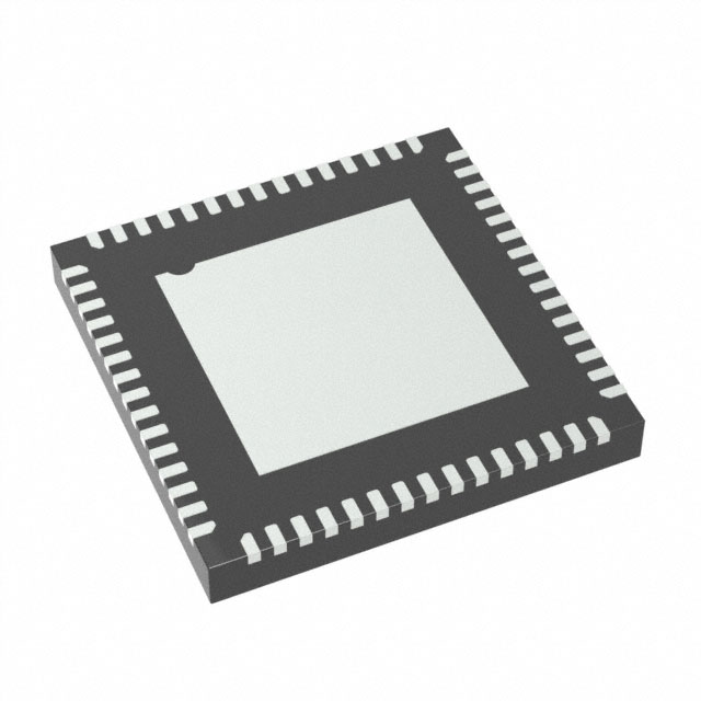
60-Pin WQFN Package, (9x9x0.8mm, 0.5mm
Pin-Pitch)
KEY SPECIFICATIONS
•
•
•
•
•
•
Resolution: 12 Bits
Conversion Rate: 105 MSPS
SNR (fIN = 170 MHz): 69 dBFS (Typ)
SFDR (fIN = 170 MHz): 83 dBFS (Typ)
Full Power Bandwidth: 1 GHz (Typ)
Power Consumption
– 690 mW (Typ), VA = 3.0V
– 800 mW (Typ), VA = 3.3V
The ADC12DC105 is available in a 60-lead WQFN
package and operates over the industrial temperature
range of −40°C to +85°C.
APPLICATIONS
•
•
•
•
•
High IF Sampling Receivers
Wireless Base Station Receivers
Test and Measurement Equipment
Communications Instrumentation
Portable Instrumentation
1
2
Please be aware that an important notice concerning availability, standard warranty, and use in critical applications of
Texas Instruments semiconductor products and disclaimers thereto appears at the end of this data sheet.
All trademarks are the property of their respective owners.
PRODUCTION DATA information is current as of publication date.
Products conform to specifications per the terms of the Texas
Instruments standard warranty. Production processing does not
necessarily include testing of all parameters.
Copyright © 2008–2013, Texas Instruments Incorporated
�ADC12DC105
SNAS469B – SEPTEMBER 2008 – REVISED MARCH 2013
www.ti.com
Block Diagram
2
12
12-Bit Pipelined
ADC Core
VINA
Output
Buffers
12
CHANNEL A
DA0-DA11
3
Ref.Decoupling
VREF
Reference
A
Timing
Generation
CLK
Ref.Decoupling
3
Reference
B
2
12-Bit Pipelined
ADC Core
VINB
12
DRDY
Output
Buffers
12
CHANNEL B
DB0-DB11
PD_A
N/C
DA11 (MSB)
DA10
DA9
DA8
DRGND
VDR
DA7
DA6
DA5
DA4
57
56
55
54
53
52
51
49
48
47
46
50
VREF
VA
58
VA
59
60
Connection Diagram
AGND
VINA-
1
45
DA3
2
44
DA2
VINA+
3
43
DA1
AGND
4
42
DA0 (LSB)
VRPA
5
41
N/C
VRNA
6
40
N/C
VCMOA
7
39
VA
8
DRDY
VDR
ADC12DC105
38
37
DRGND
36
DB11 (MSB)
11
35
DB10
12
34
DB9
13
33
DB8
32
DB7
31
DB6
20
21
22
23
24
25
26
27
28
29
30
PD_B
N/C
N/C
DB0 (LSB)
DB1
DRGND
VDR
DB2
DB3
DB4
DB5
15
OF/DCS
AGND
* Exposed Pad
18
19
14
CLK
VINB-
17
VRPB
AGND
VINB+
(top view)
16
10
VA
9
VRNB
VA
VCMOB
Figure 1. WQFN Package
See Package Number NKA0060A
2
Submit Documentation Feedback
Copyright © 2008–2013, Texas Instruments Incorporated
Product Folder Links: ADC12DC105
�ADC12DC105
www.ti.com
SNAS469B – SEPTEMBER 2008 – REVISED MARCH 2013
PIN DESCRIPTIONS
Pin No.
Symbol
Equivalent Circuit
Description
ANALOG I/O
3
13
VA
VINA+
VINB+
2
14
VINAVINB-
5
11
VRPA
VRPB
7
9
VCMOA
VCMOB
Differential analog input pins. The differential full-scale input signal
level is 2VP-P with each input pin signal centered on a common mode
voltage, VCM.
AGND
VA
VA
These pins should each be bypassed to AGND with a low ESL
(equivalent series inductance) 0.1 µF capacitor placed very close to
the pin to minimize stray inductance. An 0201 size 0.1 µF capacitor
should be placed between VRP and VRN as close to the pins as
possible, and a 1 µF capacitor should be placed in parallel.
VRP and VRN should not be loaded. VCMO may be loaded to 1mA for
use as a temperature stable 1.5V reference.
It is recommended to use VCMO to provide the common mode
voltage, VCM, for the differential analog inputs.
VA
6
10
VA
VRNA
VRNB
AGND
AGND
VA
59
Reference Voltage. This device provides an internally developed
1.2V reference. When using the internal reference, VREF should be
decoupled to AGND with a 0.1 µF and a 1µF, low equivalent series
inductance (ESL) capacitor.
This pin may be driven with an external 1.2V reference voltage.
This pin should not be used to source or sink current when the
internal reference is used.
VREF
AGND
DIGITAL I/O
VA
19
This is a four-state pin controlling the input clock mode and output
data format.
OF/DCS = VA, output data format is 2's complement without duty
cycle stabilization applied to the input clock.
OF/DCS = AGND, output data format is offset binary, without duty
cycle stabilization applied to the input clock.
OF/DCS = (2/3)*VA, output data is 2's complement with duty cycle
stabilization applied to the input clock.
OF/DCS = (1/3)*VA, output data is offset binary with duty cycle
stabilization applied to the input clock.
OF/DCS
AGND
18
CLK
57
20
PD_A
PD_B
VA
The clock input pin.
The analog inputs are sampled on the rising edge of the clock input.
This is a two-state input controlling Power Down.
PD = VA, Power Down is enabled and power dissipation is reduced.
PD = AGND, Normal operation.
AGND
Submit Documentation Feedback
Copyright © 2008–2013, Texas Instruments Incorporated
Product Folder Links: ADC12DC105
3
�ADC12DC105
SNAS469B – SEPTEMBER 2008 – REVISED MARCH 2013
www.ti.com
PIN DESCRIPTIONS (continued)
Pin No.
Symbol
Equivalent Circuit
VDR
VA
Description
Digital data output pins that make up the 12-bit conversion result for
Channel A. DA0 (pin 42) is the LSB, while DA11 (pin 55) is the MSB
of the output word. Output levels are CMOS compatible.
42-49,
52-55
DA0-DA7,
DA8-DA11
23-24,
27-36
DB0-DB1,
DB3-DB11
Digital data output pins that make up the 12-bit conversion result for
Channel B. DB0 (pin 23) is the LSB, while DB11 (pin 36) is the MSB
of the output word. Output levels are CMOS compatible.
39
DRDY
Data Ready Strobe. The data output transition is synchronized with
the falling edge of this signal. This signal switches at the same
frequency as the CLK input.
DRGND
DRGND
ANALOG POWER
8, 16, 17, 58,
60
VA
Positive analog supply pins. These pins should be connected to a
quiet source and be bypassed to AGND with 0.1 µF capacitors
located close to the power pins.
1, 4, 12, 15,
Exposed Pad
AGND
The ground return for the analog supply.
The exposed pad on back of package must be soldered to ground
plane to ensure rated performance.
26, 38,50
VDR
Positive driver supply pin for the output drivers. This pin should be
connected to a quiet voltage source and be bypassed to DRGND
with a 0.1 µF capacitor located close to the power pin.
25, 37, 51
DRGND
DIGITAL POWER
The ground return for the digital output driver supply. This pins
should be connected to the system digital ground, but not be
connected in close proximity to the ADC's AGND pins.
These devices have limited built-in ESD protection. The leads should be shorted together or the device placed in conductive foam
during storage or handling to prevent electrostatic damage to the MOS gates.
Absolute Maximum Ratings (1) (2) (3) (4) (5)
−0.3V to 4.2V
Supply Voltage (VA, VDR)
−0.3V to (VA +0.3V)
Voltage on Any Pin (Not to exceed 4.2V)
Input Current at Any Pin other than Supply Pins (6)
±5 mA
Package Input Current (6)
±50 mA
Max Junction Temp (TJ)
+150°C
Thermal Resistance (θJA)
30°C/W
ESD Rating
Human Body Model (7)
Machine Model (7)
(3)
(4)
(5)
(6)
(7)
4
250V
−65°C to +150°C
Storage Temperature
(1)
(2)
2500V
All voltages are measured with respect to GND = AGND = DRGND = 0V, unless otherwise specified.
Absolute Maximum Ratings indicate limits beyond which damage to the device may occur. Operating Ratings indicate conditions for
which the device is specified to be functional, but do not ensure specific performance limits. For ensured specifications and test
conditions, see the Electrical Characteristics. The ensured specifications apply only for the test conditions listed. Some performance
characteristics may degrade when the device is not operated under the listed test conditions. Operation of the device beyond the
maximum Operating Ratings is not recommended.
Soldering process must comply with Reflow Temperature Profile specifications. Refer to www.ti.com/packaging.
If Military/Aerospace specified devices are required, please contact the Texas Instruments Sales Office/Distributors for availability and
specifications.
Reflow temperature profiles are different for lead-free and non-lead-free packages.
When the input voltage at any pin exceeds the power supplies (that is, VIN < AGND, or VIN > VA), the current at that pin should be
limited to ±5 mA. The ±50 mA maximum package input current rating limits the number of pins that can safely exceed the power
supplies with an input current of ±5 mA to 10.
Human Body Model is 100 pF discharged through a 1.5 kΩ resistor. Machine Model is 220 pF discharged through 0 Ω.
Submit Documentation Feedback
Copyright © 2008–2013, Texas Instruments Incorporated
Product Folder Links: ADC12DC105
�ADC12DC105
www.ti.com
SNAS469B – SEPTEMBER 2008 – REVISED MARCH 2013
Operating Ratings (1) (2)
−40°C ≤ TA ≤ +85°C
Operating Temperature
Supply Voltage (VA)
+2.7V to +3.6V
Output Driver Supply (VDR)
+2.4V to VA
(DCS Enabled)
Clock Duty Cycle
30/70 %
(DCS Disabled)
45/55 %
VCM
1.4V to 1.6V
≤100mV
|AGND-DRGND|
(1)
(2)
Absolute Maximum Ratings indicate limits beyond which damage to the device may occur. Operating Ratings indicate conditions for
which the device is specified to be functional, but do not ensure specific performance limits. For ensured specifications and test
conditions, see the Electrical Characteristics. The ensured specifications apply only for the test conditions listed. Some performance
characteristics may degrade when the device is not operated under the listed test conditions. Operation of the device beyond the
maximum Operating Ratings is not recommended.
All voltages are measured with respect to GND = AGND = DRGND = 0V, unless otherwise specified.
Converter Electrical Characteristics
Unless otherwise specified, the following specifications apply: AGND = DRGND = 0V, VA = +3.3V, VDR = +2.5V, Internal VREF
= +1.2V, fCLK = 105 MHz, VCM = VCMO, CL = 5 pF/pin. Typical values are for TA = 25°C. Boldface limits apply for TMIN ≤ TA ≤
TMAX. All other limits apply for TA = 25°C (1) (2) (3)
Parameter
Test Conditions
Typical (4)
Limits
Units
(Limits)
STATIC CONVERTER CHARACTERISTICS
Resolution with No Missing Codes
12
Bits (min)
1.1
LSB (max)
-1.1
LSB (min)
0.55
LSB (max)
INL
Integral Non Linearity (5)
±0.5
DNL
Differential Non Linearity
±0.2
PGE
Positive Gain Error
NGE
Negative Gain Error
TC PGE
Positive Gain Error Tempco
−40°C ≤ TA ≤ +85°C
-3
ppm/°C
TC NGE
Negative Gain Error Tempco
−40°C ≤ TA ≤ +85°C
-7
ppm/°C
VOFF
Offset Error
TC VOFF
Offset Error Tempco
(1)
-0.55
LSB (min)
-0.1
±1
%FS (max)
0.18
±1
%FS (max)
0.01
−40°C ≤ TA ≤ +85°C
±0.55
-4
%FS (max)
ppm/°C
Under Range Output Code
0
0
Over Range Output Code
4095
4095
The inputs are protected as shown below. Input voltage magnitudes above VA or below GND will not damage this device, provided
current is limited. However, errors in the A/D conversion can occur if the input goes above 2.6V or below GND as described in the
Operating Ratings section.
VA
I/O
To Internal Circuitry
AGND
(2)
(3)
(4)
(5)
With a full scale differential input of 2VP-P , the 12-bit LSB is 488 µV.
When the input voltage at any pin exceeds the power supplies (that is, VIN < AGND, or VIN > VA), the current at that pin should be
limited to ±5 mA. The ±50 mA maximum package input current rating limits the number of pins that can safely exceed the power
supplies with an input current of ±5 mA to 10.
Typical figures are at TA = 25°C and represent most likely parametric norms at the time of product characterization. The typical
specifications are not ensured.
Integral Non Linearity is defined as the deviation of the analog value, expressed in LSBs, from the straight line that passes through
positive and negative full-scale.
Submit Documentation Feedback
Copyright © 2008–2013, Texas Instruments Incorporated
Product Folder Links: ADC12DC105
5
�ADC12DC105
SNAS469B – SEPTEMBER 2008 – REVISED MARCH 2013
www.ti.com
Converter Electrical Characteristics (continued)
Unless otherwise specified, the following specifications apply: AGND = DRGND = 0V, VA = +3.3V, VDR = +2.5V, Internal VREF
= +1.2V, fCLK = 105 MHz, VCM = VCMO, CL = 5 pF/pin. Typical values are for TA = 25°C. Boldface limits apply for TMIN ≤ TA ≤
TMAX. All other limits apply for TA = 25°C(1)(2)(3)
Parameter
Test Conditions
Typical (4)
Limits
Units
(Limits)
REFERENCE AND ANALOG INPUT CHARACTERISTICS
VCMO
Common Mode Output Voltage
1.5
1.45
1.56
V (min)
V (max)
VCM
Analog Input Common Mode Voltage
1.5
1.4
1.6
V (min)
V (max)
CIN
VIN Input Capacitance (each pin to
GND) (6)
VIN = 1.5 Vdc ± 0.5 V
(CLK LOW)
8.5
(CLK HIGH)
3.5
pF
1.176
1.224
V (min)
V (max)
VREF
Internal Reference Voltage
TC VREF
Internal Reference Voltage Tempco
18
ppm/°C
VRP
Internal Reference Top
2
V
VRN
Internal Reference Bottom
1
V
Internal Reference Accuracy
1.2
pF
−40°C ≤ TA ≤ +85°C
(VRP-VRN)
EXTVREF External Reference Voltage
(6)
1
0.89
1.06
V (Min)
V (max)
1.20
1.176
1.224
V (min)
V (max)
The input capacitance is the sum of the package/pin capacitance and the sample and hold circuit capacitance.
Dynamic Converter Electrical Characteristics
Unless otherwise specified, the following specifications apply: AGND = DRGND = 0V, VA = +3.3V, VDR = +2.5V, Internal VREF
= +1.2V, fCLK = 105 MHz, VCM = VCMO, CL = 5 pF/pin, . Typical values are for TA = 25°C. Boldface limits apply for TMIN ≤ TA
≤ TMAX. All other limits apply for TA = 25°C (1) (2)
Parameter
Test Conditions
Typical (3)
Limits
Units
(Limits) (4)
DYNAMIC CONVERTER CHARACTERISTICS, AIN= -1dBFS
FPBW
SNR
SFDR
ENOB
(1)
(2)
(3)
(4)
6
Full Power Bandwidth
Signal-to-Noise Ratio
Spurious Free Dynamic Range
Effective Number of Bits
-1 dBFS Input, −3 dB Corner
1.0
GHz
fIN = 10 MHz
71
dBFS
fIN = 70 MHz
70.5
dBFS
fIN =170 MHz
69.1
fIN = 240 MHz
68.5
dBFS
fIN = 10 MHz
90
dBFS
fIN = 70 MHz
86
fIN = 170 MHz
83
fIN = 240 MHz
81
dBFS
fIN = 10 MHz
11.5
Bits
fIN = 70 MHz
11.4
fIN = 170 MHz
11.2
fIN = 240 MHz
11
68
dBFS
dBFS
78
dBFS
Bits
10.9
Bits
dBFS
All voltages are measured with respect to GND = AGND = DRGND = 0V, unless otherwise specified.
Absolute Maximum Ratings indicate limits beyond which damage to the device may occur. Operating Ratings indicate conditions for
which the device is specified to be functional, but do not ensure specific performance limits. For ensured specifications and test
conditions, see the Electrical Characteristics. The ensured specifications apply only for the test conditions listed. Some performance
characteristics may degrade when the device is not operated under the listed test conditions. Operation of the device beyond the
maximum Operating Ratings is not recommended.
Typical figures are at TA = 25°C and represent most likely parametric norms at the time of product characterization. The typical
specifications are not ensured.
This parameter is specified in units of dBFS - indicating the value that would be attained with a full-scale input signal.
Submit Documentation Feedback
Copyright © 2008–2013, Texas Instruments Incorporated
Product Folder Links: ADC12DC105
�ADC12DC105
www.ti.com
SNAS469B – SEPTEMBER 2008 – REVISED MARCH 2013
Dynamic Converter Electrical Characteristics (continued)
Unless otherwise specified, the following specifications apply: AGND = DRGND = 0V, VA = +3.3V, VDR = +2.5V, Internal VREF
= +1.2V, fCLK = 105 MHz, VCM = VCMO, CL = 5 pF/pin, . Typical values are for TA = 25°C. Boldface limits apply for TMIN ≤ TA
≤ TMAX. All other limits apply for TA = 25°C(1)(2)
Parameter
THD
H2
Total Harmonic Disortion
Second Harmonic Distortion
H3
Third Harmonic Distortion
Test Conditions
Typical (3)
Limits
Units
(Limits) (4)
fIN = 10 MHz
−86
fIN = 70 MHz
−85
fIN = 170 MHz
−84
fIN = 240 MHz
-80
dBFS
fIN = 10 MHz
−95
dBFS
fIN = 70 MHz
−90
fIN = 170 MHz
−83
fIN = 240 MHz
-84
dBFS
fIN = 10 MHz
−90
dBFS
fIN = 70 MHz
−86
fIN = 170 MHz
−83
dBFS
dBFS
-76.5
dBFS
dBFS
-78
dBFS
dBFS
-78
dBFS
fIN = 240 MHz
-81
dBFS
fIN = 10 MHz
70.9
dBFS
fIN = 70 MHz
70.3
fIN = 170 MHz
69
dBFS
SINAD
Signal-to-Noise and Distortion Ratio
fIN = 240 MHz
68.2
dBFS
IMD
Intermodulation Distortion
fIN = 20 MHz and 21 MHz, each -7dBFS
-84
dBFS
Crosstalk
0 MHz tested channel, fIN = 10 MHz at 1dBFS other channel
-100
dBFS
67.4
dBFS
Logic and Power Supply Electrical Characteristics
Unless otherwise specified, the following specifications apply: AGND = DRGND = 0V, VA = +3.3V, VDR = +2.5V, Internal VREF
= +1.2V, fCLK = 105 MHz, VCM = VCMO, CL = 5 pF/pin. Typical values are for TA = 25°C. Boldface limits apply for TMIN ≤ TA ≤
TMAX. All other limits apply for TA = 25°C (1) (2) (3)
Parameter
Test Conditions
Typical (4)
Limits
Units
(Limits)
DIGITAL INPUT CHARACTERISTICS (CLK, PD_A,PD_B)
VIN(1)
Logical “1” Input Voltage
VD = 3.3V
2.0
V (min)
VIN(0)
Logical “0” Input Voltage
VD = 3.0V
0.8
V (max)
IIN(1)
Logical “1” Input Current
VIN = 3.3V
10
µA
IIN(0)
Logical “0” Input Current
VIN = 0V
−10
µA
CIN
Digital Input Capacitance
5
pF
(1)
The inputs are protected as shown below. Input voltage magnitudes above VA or below GND will not damage this device, provided
current is limited. However, errors in the A/D conversion can occur if the input goes above 2.6V or below GND as described in the
Operating Ratings section.
VA
I/O
To Internal Circuitry
AGND
(2)
(3)
(4)
With a full scale differential input of 2VP-P , the 12-bit LSB is 488 µV.
When the input voltage at any pin exceeds the power supplies (that is, VIN < AGND, or VIN > VA), the current at that pin should be
limited to ±5 mA. The ±50 mA maximum package input current rating limits the number of pins that can safely exceed the power
supplies with an input current of ±5 mA to 10.
Typical figures are at TA = 25°C and represent most likely parametric norms at the time of product characterization. The typical
specifications are not ensured.
Submit Documentation Feedback
Copyright © 2008–2013, Texas Instruments Incorporated
Product Folder Links: ADC12DC105
7
�ADC12DC105
SNAS469B – SEPTEMBER 2008 – REVISED MARCH 2013
www.ti.com
Logic and Power Supply Electrical Characteristics (continued)
Unless otherwise specified, the following specifications apply: AGND = DRGND = 0V, VA = +3.3V, VDR = +2.5V, Internal VREF
= +1.2V, fCLK = 105 MHz, VCM = VCMO, CL = 5 pF/pin. Typical values are for TA = 25°C. Boldface limits apply for TMIN ≤ TA ≤
TMAX. All other limits apply for TA = 25°C(1)(2)(3)
Parameter
Test Conditions
Typical (4)
Limits
Units
(Limits)
DIGITAL OUTPUT CHARACTERISTICS (DA0-DA11,DB0-DB11,DRDY)
VOUT(1)
Logical “1” Output Voltage
IOUT = −0.5 mA , VDR = 2.4V
2.0
V (min)
VOUT(0)
Logical “0” Output Voltage
IOUT = 1.6 mA, VDR = 2.4V
0.4
V (max)
+ISC
Output Short Circuit Source Current
VOUT = 0V
−10
mA
−ISC
Output Short Circuit Sink Current
VOUT = VDR
10
mA
COUT
Digital Output Capacitance
5
pF
POWER SUPPLY CHARACTERISTICS
IA
Analog Supply Current
IDR
(5)
Full Operation
242
(5)
Digital Output Supply Current
Full Operation
Power Consumption
Excludes IDR (5)
800
Power Down Power Consumption
PD_A=PD_B=VA
33
273
mA (max)
900
mW (max)
32
mA
mW
IDR is the current consumed by the switching of the output drivers and is primarily determined by load capacitance on the output pins,
the supply voltage, VDR, and the rate at which the outputs are switching (which is signal dependent). IDR=VDR(C0 x f0 + C1 x f1 +....C11 x
f11) where VDR is the output driver power supply voltage, Cn is total capacitance on the output pin, and fn is the average frequency at
which that pin is toggling.
Timing and AC Characteristics
Unless otherwise specified, the following specifications apply: AGND = DRGND = 0V, VA = +3.3V, VDR = +2.5V, Internal VREF
= +1.2V, fCLK = 105 MHz, VCM = VCMO, CL = 5 pF/pin. Typical values are for TA = 25°C. Timing measurements are taken at
50% of the signal amplitude. Boldface limits apply for TMIN ≤ TA ≤ TMAX. All other limits apply for TA = 25°C (1) (2) (3)
Limits
Units
(Limits)
Maximum Clock Frequency
105
MHz (max)
Minimum Clock Frequency
20
MHz (min)
Parameter
Test Conditions
Typical (4)
tCH
Clock High Time
4
tCL
Clock Low Time
4
tCONV
Conversion Latency
tOD
Output Delay of CLK to DATA
Relative to rising edge of CLK
tSU
Data Output Setup Time
Relative to DRDY
tH
Data Output Hold Time
Relative to DRDY
tAD
Aperture Delay
0.6
ns
tAJ
Aperture Jitter
0.1
ps rms
(1)
ns
ns
7
Clock Cycles
4.6
8.8
ns (min)
ns (max)
4
3
ns (min)
5.5
3.8
ns (min)
6.7
The inputs are protected as shown below. Input voltage magnitudes above VA or below GND will not damage this device, provided
current is limited. However, errors in the A/D conversion can occur if the input goes above 2.6V or below GND as described in the
Operating Ratings section.
VA
I/O
To Internal Circuitry
AGND
(2)
(3)
(4)
8
With a full scale differential input of 2VP-P , the 12-bit LSB is 488 µV.
When the input voltage at any pin exceeds the power supplies (that is, VIN < AGND, or VIN > VA), the current at that pin should be
limited to ±5 mA. The ±50 mA maximum package input current rating limits the number of pins that can safely exceed the power
supplies with an input current of ±5 mA to 10.
Typical figures are at TA = 25°C and represent most likely parametric norms at the time of product characterization. The typical
specifications are not ensured.
Submit Documentation Feedback
Copyright © 2008–2013, Texas Instruments Incorporated
Product Folder Links: ADC12DC105
�ADC12DC105
www.ti.com
SNAS469B – SEPTEMBER 2008 – REVISED MARCH 2013
Specification Definitions
APERTURE DELAY is the time after the falling edge of the clock to when the input signal is acquired or held for
conversion.
APERTURE JITTER (APERTURE UNCERTAINTY) is the variation in aperture delay from sample to sample.
Aperture jitter manifests itself as noise in the output.
CLOCK DUTY CYCLE is the ratio of the time during one cycle that a repetitive digital waveform is high to the
total time of one period. The specification here refers to the ADC clock input signal.
COMMON MODE VOLTAGE (VCM) is the common DC voltage applied to both input terminals of the ADC.
CONVERSION LATENCY is the number of clock cycles between initiation of conversion and when that data is
presented to the output driver stage. Data for any given sample is available at the output pins the Pipeline Delay
plus the Output Delay after the sample is taken. New data is available at every clock cycle, but the data lags the
conversion by the pipeline delay.
CROSSTALK is coupling of energy from one channel into the other channel.
DIFFERENTIAL NON-LINEARITY (DNL) is the measure of the maximum deviation from the ideal step size of 1
LSB.
EFFECTIVE NUMBER OF BITS (ENOB, or EFFECTIVE BITS) is another method of specifying Signal-to-Noise
and Distortion Ratio or SINAD. ENOB is defined as (SINAD - 1.76) / 6.02 and says that the converter is
equivalent to a perfect ADC of this (ENOB) number of bits.
FULL POWER BANDWIDTH is a measure of the frequency at which the reconstructed output fundamental
drops 3 dB below its low frequency value for a full scale input.
GAIN ERROR is the deviation from the ideal slope of the transfer function. It can be calculated as:
Gain Error = Positive Full Scale Error − Negative Full Scale Error
(1)
It can also be expressed as Positive Gain Error and Negative Gain Error, which are calculated as:
PGE = Positive Full Scale Error - Offset Error NGE = Offset Error - Negative Full Scale Error
(2)
INTEGRAL NON LINEARITY (INL) is a measure of the deviation of each individual code from a best fit straight
line. The deviation of any given code from this straight line is measured from the center of that code value.
INTERMODULATION DISTORTION (IMD) is the creation of additional spectral components as a result of two
sinusoidal frequencies being applied to the ADC input at the same time. It is defined as the ratio of the power in
the intermodulation products to the total power in the original frequencies. IMD is usually expressed in dBFS.
LSB (LEAST SIGNIFICANT BIT) is the bit that has the smallest value or weight of all bits. This value is VFS/2n,
where “VFS” is the full scale input voltage and “n” is the ADC resolution in bits.
MISSING CODES are those output codes that will never appear at the ADC outputs. The ADC is ensured not to
have any missing codes.
MSB (MOST SIGNIFICANT BIT) is the bit that has the largest value or weight. Its value is one half of full scale.
NEGATIVE FULL SCALE ERROR is the difference between the actual first code transition and its ideal value of
½ LSB above negative full scale.
OFFSET ERROR is the difference between the two input voltages [(VIN+) – (VIN-)] required to cause a transition
from code 2047 to 2048.
OUTPUT DELAY is the time delay after the falling edge of the clock before the data update is presented at the
output pins.
PIPELINE DELAY (LATENCY) See CONVERSION LATENCY.
POSITIVE FULL SCALE ERROR is the difference between the actual last code transition and its ideal value of
1½ LSB below positive full scale.
POWER SUPPLY REJECTION RATIO (PSRR) is a measure of how well the ADC rejects a change in the power
supply voltage. PSRR is the ratio of the Full-Scale output of the ADC with the supply at the minimum DC supply
limit to the Full-Scale output of the ADC with the supply at the maximum DC supply limit, expressed in dB.
Submit Documentation Feedback
Copyright © 2008–2013, Texas Instruments Incorporated
Product Folder Links: ADC12DC105
9
�ADC12DC105
SNAS469B – SEPTEMBER 2008 – REVISED MARCH 2013
www.ti.com
SIGNAL TO NOISE RATIO (SNR) is the ratio, expressed in dB, of the rms value of the input signal to the rms
value of the sum of all other spectral components below one-half the sampling frequency, not including
harmonics or DC.
SIGNAL TO NOISE PLUS DISTORTION (S/N+D or SINAD) Is the ratio, expressed in dB, of the rms value of the
input signal to the rms value of all of the other spectral components below half the clock frequency, including
harmonics but excluding d.c.
SPURIOUS FREE DYNAMIC RANGE (SFDR) is the difference, expressed in dB, between the rms values of the
input signal and the peak spurious signal, where a spurious signal is any signal present in the output spectrum
that is not present at the input.
TOTAL HARMONIC DISTORTION (THD) is the ratio, expressed in dB, of the rms total of the first six harmonic
levels at the output to the level of the fundamental at the output. THD is calculated as:
(3)
where f1 is the RMS power of the fundamental (output) frequency and f2 through f7 are the RMS power of the first
6 harmonic frequencies in the output spectrum.
SECOND HARMONIC DISTORTION (2ND HARM) is the difference expressed in dB, between the RMS power in
the input frequency at the output and the power in its 2nd harmonic level at the output.
THIRD HARMONIC DISTORTION (3RD HARM) is the difference, expressed in dB, between the RMS power in
the input frequency at the output and the power in its 3rd harmonic level at the output.
Timing Diagrams
Sample N
Sample N + 9
Sample N + 10
|
VINA
Sample N + 8
Sample N + 7
Sample N + 6
VINB
tAD
Clock N
1
FCLK
Clock N + 7
90%
CLK
|
10%
tCH
tCL
90%
10%
tf
tr
DRDY
|
Latency ( tCONV )
tOD
| |
DA0 - DA11
DB0 - DB11
Data N - 1
Data N + 1
Data N
tSU
Data N + 2
tH
Figure 2. Output Timing
10
Submit Documentation Feedback
Copyright © 2008–2013, Texas Instruments Incorporated
Product Folder Links: ADC12DC105
�ADC12DC105
www.ti.com
SNAS469B – SEPTEMBER 2008 – REVISED MARCH 2013
Transfer Characteristic
Figure 3. Transfer Characteristic
Typical Performance Characteristics DNL, INL
Unless otherwise specified, the following specifications apply: AGND = DRGND = 0V, VA = +3.3V, VDR = +2.5V, Internal VREF
= +1.2V, fCLK = 105 MHz, 50% Duty Cycle, DCS disabled, VCM = VCMO, TA = 25°C.
DNL
INL
Figure 4.
Figure 5.
Submit Documentation Feedback
Copyright © 2008–2013, Texas Instruments Incorporated
Product Folder Links: ADC12DC105
11
�ADC12DC105
SNAS469B – SEPTEMBER 2008 – REVISED MARCH 2013
www.ti.com
Typical Performance Characteristics
Unless otherwise specified, the following specifications apply: AGND = DRGND = 0V, VA = +3.3V, VDR = +2.5V, Internal VREF
= +1.2V, fCLK = 105 MHz, 50% Duty Cycle, DCS disabled, VCM = VCMO, fIN = 170 MHz, TA = 25°C.
12
SNR, SINAD, SFDR vs. VA
Distortion vs. VA
Figure 6.
Figure 7.
SNR, SINAD, SFDR vs. Clock Duty Cycle, fIN=40 MHz
Distortion vs. Clock Duty Cycle, fIN=40 MHz
Figure 8.
Figure 9.
SNR, SINAD, SFDR vs. Clock Duty Cycle, DCS Enabled,
fIN=40 MHz
Distortion vs. Clock Duty Cycle, DCS Enabled, fIN=40 MHz
Figure 10.
Figure 11.
Submit Documentation Feedback
Copyright © 2008–2013, Texas Instruments Incorporated
Product Folder Links: ADC12DC105
�ADC12DC105
www.ti.com
SNAS469B – SEPTEMBER 2008 – REVISED MARCH 2013
Typical Performance Characteristics (continued)
Unless otherwise specified, the following specifications apply: AGND = DRGND = 0V, VA = +3.3V, VDR = +2.5V, Internal VREF
= +1.2V, fCLK = 105 MHz, 50% Duty Cycle, DCS disabled, VCM = VCMO, fIN = 170 MHz, TA = 25°C.
SNR and SFDR vs. fIN
POWER vs. fCLK
Figure 12.
Figure 13.
Spectral Response @ 10 MHz Input
Spectral Response @ 70 MHz Input
Figure 14.
Figure 15.
Spectral Response @ 170 MHz Input
IMD, fIN1 = 20 MHz, fIN2 = 21 MHz
Figure 16.
Figure 17.
Submit Documentation Feedback
Copyright © 2008–2013, Texas Instruments Incorporated
Product Folder Links: ADC12DC105
13
�ADC12DC105
SNAS469B – SEPTEMBER 2008 – REVISED MARCH 2013
www.ti.com
FUNCTIONAL DESCRIPTION
Operating on a single +3.0V or +3.3V supply, the ADC12DC105 digitizes two differential analog input signals to
12 bits, using a differential pipelined architecture with error correction circuitry and an on-chip sample-and-hold
circuit to ensure maximum performance. The user has the choice of using an internal 1.2V stable reference, or
using an external 1.2V reference. Any external reference is buffered on-chip to ease the task of driving that pin.
Duty cycle stabilization and output data format are selectable using the quad state function OF/DCS pin (pin 19).
The output data can be set for offset binary or two's complement.
APPLICATIONS INFORMATION
OPERATING CONDITIONS
We recommend that the following conditions be observed for operation of the ADC12DC105:
2.7V ≤ VA ≤ 3.6V
2.4V ≤ VDR ≤ VA
20 MHz ≤ fCLK ≤ 105 MHz
1.2V internal reference
VREF = 1.2V (for an external reference)
VCM = 1.5V (from VCMO)
ANALOG INPUTS
Signal Inputs
Differential Analog Input Pins
The ADC12DC105 has a pair of analog signal input pins for each of two channels. VIN+ and VIN− form a
differential input pair. The input signal, VIN, is defined as:
VIN = (VIN+) – (VIN−)
(4)
Figure 18 shows the expected input signal range. Note that the common mode input voltage, VCM, should be
1.5V. Using VCMO (pins 7,9) for VCM will ensure the proper input common mode level for the analog input signal.
The positive peaks of the individual input signals should each never exceed 2.6V. Each analog input pin of the
differential pair should have a maximum peak-to-peak voltage of 1V, be 180° out of phase with each other and
be centered around VCM.The peak-to-peak voltage swing at each analog input pin should not exceed the 1V or
the output data will be clipped.
Figure 18. Expected Input Signal Range
14
Submit Documentation Feedback
Copyright © 2008–2013, Texas Instruments Incorporated
Product Folder Links: ADC12DC105
�ADC12DC105
www.ti.com
SNAS469B – SEPTEMBER 2008 – REVISED MARCH 2013
For single frequency sine waves the full scale error in LSB can be described as approximately:
EFS = 4096 ( 1 - sin (90° + dev))
where
•
dev is the angular difference in degrees between the two signals having a 180° relative phase relationship to
each other (see Figure 19)
(5)
For single frequency inputs, angular errors result in a reduction of the effective full scale input. For complex
waveforms, however, angular errors will result in distortion.
Figure 19. Angular Errors Between the Two Input Signals Will Reduce the Output Level or Cause
Distortion
It is recommended to drive the analog inputs with a source impedance less than 100Ω. Matching the source
impedance for the differential inputs will improve even ordered harmonic performance (particularly second
harmonic).
Table 1 indicates the input to output relationship of the ADC12DC105.
Table 1. Input to Output Relationship
VIN+
VIN−
Binary Output
2’s Complement Output
VCM − VREF/2
VCM + VREF/2
00 0000 0000 00
10 0000 0000 00
VCM − VREF/4
VCM + VREF/4
01 0000 0000 00
11 0000 0000 00
VCM
VCM
10 0000 0000 00
00 0000 0000 00
VCM + VREF/4
VCM − VREF/4
11 0000 0000 00
01 0000 0000 00
VCM + VREF/2
VCM − VREF/2
11 1111 1111 11
01 1111 1111 11
Negative Full-Scale
Mid-Scale
Positive Full-Scale
Submit Documentation Feedback
Copyright © 2008–2013, Texas Instruments Incorporated
Product Folder Links: ADC12DC105
15
�ADC12DC105
SNAS469B – SEPTEMBER 2008 – REVISED MARCH 2013
www.ti.com
Driving the Analog Inputs
The VIN+ and the VIN− inputs of the ADC12DC105 have an internal sample-and-hold circuit which consists of an
analog switch followed by a switched-capacitor amplifier.
Figure 20 and Figure 21 show examples of single-ended to differential conversion circuits. The circuit in
Figure 20 works well for input frequencies up to approximately 70MHz, while the circuit in Figure 21 works well
above 70MHz.
VIN
0.1 PF
20:
ADT1-1WT
18 pF
50:
ADC
Input
0.1 PF
0.1 PF
20:
VCMO
Figure 20. Low Input Frequency Transformer Drive Circuit
VIN
0.1 PF
ETC1-1-13
100:
3 pF
0.1 PF
ADC
Input
100:
ETC1-1-13
VCMO
0.1 PF
Figure 21. High Input Frequency Transformer Drive Circuit
One short-coming of using a transformer to achieve the single-ended to differential conversion is that most RF
transformers have poor low frequency performance. A differential amplifier can be used to drive the analog inputs
for low frequency applications. The amplifier must be fast enough to settle from the charging glitches on the
analog input resulting from the sample-and-hold operation before the clock goes high and the sample is passed
to the ADC core.
Input Common Mode Voltage
The input common mode voltage, VCM, should be in the range of 1.4V to 1.6V and be a value such that the peak
excursions of the analog signal do not go more negative than ground or more positive than 2.6V. It is
recommended to use VCMO (pins 7,9) as the input common mode voltage.
If the ADC12DC105 is operated with VA=3.6V, a resistor of approximately 1KΩ should be used from the VCMO pin
to AGND. This will help maintain stability over the entire temperature range when using a high supply voltage.
Reference Pins
The ADC12DC105 is designed to operate with an internal or external 1.2V reference. The internal 1.2 Volt
reference is the default condition when no external reference input is applied to the VREF pin. If a voltage is
applied to the VREF pin, then that voltage is used for the reference. The VREF pin should always be bypassed to
ground with a 0.1 µF capacitor close to the reference input pin. Do not load this pin when using the internal
reference.
It is important that all grounds associated with the reference voltage and the analog input signal make connection
to the ground plane at a single, quiet point to minimize the effects of noise currents in the ground path.
The Reference Bypass Pins (VRP, VCMO, and VRN) for channels A and B are made available for bypass purposes.
These pins should each be bypassed to AGND with a low ESL (equivalent series inductance) 0.1 µF capacitor
placed very close to the pin to minimize stray inductance. A 0.1 µF capacitor should be placed between VRP and
VRN as close to the pins as possible, and a 1 µF capacitor should be placed in parallel. This configuration is
shown in Figure 22. It is necessary to avoid reference oscillation, which could result in reduced SFDR and/or
SNR. VCMO may be loaded to 1mA for use as a temperature stable 1.5V reference. The remaining pins should
not be loaded.
16
Submit Documentation Feedback
Copyright © 2008–2013, Texas Instruments Incorporated
Product Folder Links: ADC12DC105
�ADC12DC105
www.ti.com
SNAS469B – SEPTEMBER 2008 – REVISED MARCH 2013
Smaller capacitor values than those specified will allow faster recovery from the power down mode, but may
result in degraded noise performance. Loading any of these pins, other than VCMO may result in performance
degradation.
The nominal voltages for the reference bypass pins are as follows:
VCMO = 1.5 V
VRP = 2.0 V
VRN = 1.0 V
OF/DCS Pin
Duty cycle stabilization and output data format are selectable using this quad state function pin. When enabled,
duty cycle stabilization can compensate for clock inputs with duty cycles ranging from 30% to 70% and generate
a stable internal clock, improving the performance of the part. With OF/DCS = VA the output data format is 2's
complement and duty cycle stabilization is not used. With OF/DCS = AGND the output data format is offset
binary and duty cycle stabilization is not used. With OF/DCS = (2/3)*VA the output data format is 2's complement
and duty cycle stabilization is applied to the clock. If OF/DCS is (1/3)*VA the output data format is offset binary
and duty cycle stabilization is applied to the clock. While the sense of this pin may be changed "on the fly," doing
this is not recommended as the output data could be erroneous for a few clock cycles after this change is made.
Note: This signal has no effect when SPI_EN is high and the serial control interface is enabled.
DIGITAL INPUTS
Digital CMOS compatible inputs consist of CLK, PD_A, and PD_B.
Clock Input
The CLK controls the timing of the sampling process. To achieve the optimum noise performance, the clock input
should be driven with a stable, low jitter clock signal in the range indicated in the Electrical Table. The clock input
signal should also have a short transition region. This can be achieved by passing a low-jitter sinusoidal clock
source through a high speed buffer gate. The trace carrying the clock signal should be as short as possible and
should not cross any other signal line, analog or digital, not even at 90°.
The clock signal also drives an internal state machine. If the clock is interrupted, or its frequency is too low, the
charge on the internal capacitors can dissipate to the point where the accuracy of the output data will degrade.
This is what limits the minimum sample rate.
The clock line should be terminated at its source in the characteristic impedance of that line. Take care to
maintain a constant clock line impedance throughout the length of the line. Refer to Application Note AN-905
(SNLA035) for information on setting characteristic impedance.
It is highly desirable that the the source driving the ADC clock pins only drive that pin. However, if that source is
used to drive other devices, then each driven pin should be AC terminated with a series RC to ground, such that
the resistor value is equal to the characteristic impedance of the clock line and the capacitor value is:
where
•
•
•
tPD is the signal propagation rate down the clock line
"L" is the line length
ZO is the characteristic impedance of the clock line
(6)
This termination should be as close as possible to the ADC clock pin but beyond it as seen from the clock
source. Typical tPD is about 150 ps/inch (60 ps/cm) on FR-4 board material. The units of "L" and tPD should be
the same (inches or centimeters).
The duty cycle of the clock signal can affect the performance of the A/D Converter. Because achieving a precise
duty cycle is difficult, the ADC12DC105 has a Duty Cycle Stabilizer.
Submit Documentation Feedback
Copyright © 2008–2013, Texas Instruments Incorporated
Product Folder Links: ADC12DC105
17
�ADC12DC105
SNAS469B – SEPTEMBER 2008 – REVISED MARCH 2013
www.ti.com
DIGITAL OUTPUTS
Digital outputs consist of the CMOS signals DA0-DA11, DB0-DB11, and DRDY.
The ADC12DC105 has 12 CMOS compatible data output pins corresponding to the converted input value for
each channel, and a data ready (DRDY) signal that should be used to capture the output data. Valid data is
present at these outputs while the PD pin is low. Data should be captured and latched with the rising edge of the
DRDY signal.
Be very careful when driving a high capacitance bus. The more capacitance the output drivers must charge for
each conversion, the more instantaneous digital current flows through VDR and DRGND. These large charging
current spikes can cause on-chip ground noise and couple into the analog circuitry, degrading dynamic
performance. Adequate bypassing, limiting output capacitance and careful attention to the ground plane will
reduce this problem. The result could be an apparent reduction in dynamic performance.
+3.3V
+2.5V
3x 0.1 PF
5x 0.1 PF
+
7
0.1 PF
5
0.1 PF
0.1 PF
1 PF
6
9
0.1 PF
11
0.1 PF 10
1
0.1 PF
20
0.1 PF
26
38
50
VREF
VCMOA
(MSB )
DA11
DA10
DA9
DA8
55
54
53
52
49
DA7
48
DA6
DA5 47
46
DA4
45
DA3
44
DA2
DA1 43
(LSB) DA0 42
VRPA
VRNA
0.1 PF
50
VIN_A
VDR
VDR
VDR
59
8
16
17
58
60
0.1 PF
VA
VA
VA
VA
VA
10 PF
1 PF
VCMOB
VRPB
VRNB
0.1 PF
0.1 PF
3
2
2
18 pF
0.1 PF
20
VINA+
VINA-
ADT1-1WT
50
DRDY
39
22:
Channel A
Output Word
74LCX162244
22:
Buffered
DRDY
ADC12DC105
VIN_B
1
20
0.1 PF
(MSB )
DA11
DB10
DB9
DB8
0.1 PF
2
18 pF
0.1 PF
20
13
14
VINB+
VINB-
ADT1-1WT
Crystal Oscillator
18
OF/DCS
19
57
PD_A
20
PD_B
DB7
DB6
DB5
CLK
DB4
DB3
DB2
DB1
OF/DCS
PD_A
PD_B
22:
Channel B
Output Word
DR GND
DR GND
DR GND
74LCX162244
25
37
51
1
4
12
15
AGND
AGND
AGND
AGND
(LSB) DB0
36
35
34
33
32
31
30
29
28
27
24
23
Figure 22. Application Circuit
POWER SUPPLY CONSIDERATIONS
The power supply pins should be bypassed with a 0.1 µF capacitor and with a 100 pF ceramic chip capacitor
close to each power pin. Leadless chip capacitors are preferred because they have low series inductance.
As is the case with all high-speed converters, the ADC12DC105 is sensitive to power supply noise. Accordingly,
the noise on the analog supply pin should be kept below 100 mVP-P.
No pin should ever have a voltage on it that is in excess of the supply voltages, not even on a transient basis. Be
especially careful of this during power turn on and turn off.
18
Submit Documentation Feedback
Copyright © 2008–2013, Texas Instruments Incorporated
Product Folder Links: ADC12DC105
�ADC12DC105
www.ti.com
SNAS469B – SEPTEMBER 2008 – REVISED MARCH 2013
LAYOUT AND GROUNDING
Proper grounding and proper routing of all signals are essential to ensure accurate conversion. Maintaining
separate analog and digital areas of the board, with the ADC12DC105 between these areas, is required to
achieve specified performance.
Capacitive coupling between the typically noisy digital circuitry and the sensitive analog circuitry can lead to poor
performance. The solution is to keep the analog circuitry separated from the digital circuitry, and to keep the
clock line as short as possible.
Since digital switching transients are composed largely of high frequency components, total ground plane copper
weight will have little effect upon the logic-generated noise. This is because of the skin effect. Total surface area
is more important than is total ground plane area.
Generally, analog and digital lines should cross each other at 90° to avoid crosstalk. To maximize accuracy in
high speed, high resolution systems, however, avoid crossing analog and digital lines altogether. It is important to
keep clock lines as short as possible and isolated from ALL other lines, including other digital lines. Even the
generally accepted 90° crossing should be avoided with the clock line as even a little coupling can cause
problems at high frequencies. This is because other lines can introduce jitter into the clock line, which can lead to
degradation of SNR. Also, the high speed clock can introduce noise into the analog chain.
Best performance at high frequencies and at high resolution is obtained with a straight signal path. That is, the
signal path through all components should form a straight line wherever possible.
Be especially careful with the layout of inductors and transformers. Mutual inductance can change the
characteristics of the circuit in which they are used. Inductors and transformers should not be placed side by
side, even with just a small part of their bodies beside each other. For instance, place transformers for the analog
input and the clock input at 90° to one another to avoid magnetic coupling.
The analog input should be isolated from noisy signal traces to avoid coupling of spurious signals into the input.
Any external component (e.g., a filter capacitor) connected between the converter's input pins and ground or to
the reference input pin and ground should be connected to a very clean point in the ground plane.
All analog circuitry (input amplifiers, filters, reference components, etc.) should be placed in the analog area of
the board. All digital circuitry and dynamic I/O lines should be placed in the digital area of the board. The
ADC12DC105 should be between these two areas. Furthermore, all components in the reference circuitry and
the input signal chain that are connected to ground should be connected together with short traces and enter the
ground plane at a single, quiet point. All ground connections should have a low inductance path to ground.
DYNAMIC PERFORMANCE
To achieve the best dynamic performance, the clock source driving the CLK input must have a sharp transition
region and be free of jitter. Isolate the ADC clock from any digital circuitry with buffers, as with the clock tree
shown in Figure 23. The gates used in the clock tree must be capable of operating at frequencies much higher
than those used if added jitter is to be prevented.
As mentioned in Section Clock Input, it is good practice to keep the ADC clock line as short as possible and to
keep it well away from any other signals. Other signals can introduce jitter into the clock signal, which can lead to
reduced SNR performance, and the clock can introduce noise into other lines. Even lines with 90° crossings
have capacitive coupling, so try to avoid even these 90° crossings of the clock line.
Figure 23. Isolating the ADC Clock from other Circuitry with a Clock Tree
Submit Documentation Feedback
Copyright © 2008–2013, Texas Instruments Incorporated
Product Folder Links: ADC12DC105
19
�ADC12DC105
SNAS469B – SEPTEMBER 2008 – REVISED MARCH 2013
www.ti.com
REVISION HISTORY
Changes from Revision A (March 2013) to Revision B
•
20
Page
Changed layout of National Data Sheet to TI format .......................................................................................................... 19
Submit Documentation Feedback
Copyright © 2008–2013, Texas Instruments Incorporated
Product Folder Links: ADC12DC105
�PACKAGE OPTION ADDENDUM
www.ti.com
10-Dec-2020
PACKAGING INFORMATION
Orderable Device
Status
(1)
Package Type Package Pins Package
Drawing
Qty
Eco Plan
(2)
Lead finish/
Ball material
MSL Peak Temp
Op Temp (°C)
Device Marking
(3)
(4/5)
(6)
ADC12DC105CISQ/NOPB
ACTIVE
WQFN
NKA
60
2000
RoHS & Green
SN
Level-3-260C-168 HR
-45 to 85
12DC105
CISQ
ADC12DC105CISQE/NOPB
ACTIVE
WQFN
NKA
60
250
RoHS & Green
SN
Level-3-260C-168 HR
-45 to 85
12DC105
CISQ
(1)
The marketing status values are defined as follows:
ACTIVE: Product device recommended for new designs.
LIFEBUY: TI has announced that the device will be discontinued, and a lifetime-buy period is in effect.
NRND: Not recommended for new designs. Device is in production to support existing customers, but TI does not recommend using this part in a new design.
PREVIEW: Device has been announced but is not in production. Samples may or may not be available.
OBSOLETE: TI has discontinued the production of the device.
(2)
RoHS: TI defines "RoHS" to mean semiconductor products that are compliant with the current EU RoHS requirements for all 10 RoHS substances, including the requirement that RoHS substance
do not exceed 0.1% by weight in homogeneous materials. Where designed to be soldered at high temperatures, "RoHS" products are suitable for use in specified lead-free processes. TI may
reference these types of products as "Pb-Free".
RoHS Exempt: TI defines "RoHS Exempt" to mean products that contain lead but are compliant with EU RoHS pursuant to a specific EU RoHS exemption.
Green: TI defines "Green" to mean the content of Chlorine (Cl) and Bromine (Br) based flame retardants meet JS709B low halogen requirements of