User's Guide
SNAU010A – December 2005 – Revised August 2014
ADC12D040, ADC11DL066, ADC12DL066 - A/D Converters
with Internal Reference and Sample & Hold
Evaluation Board User’s Guide
ADC12D040 Dual 12-Bit, 40 MSPS, 5 Volt, 600 mW
ADC11DL066 Dual 11-Bit, 66 MSPS 3.3 Volt, 862 mW
ADC12DL066 Dual 12-Bit, 66 MSPS 3.3 Volt, 862 mW
SNAU010A – December 2005 – Revised August 2014
Submit Documentation Feedback
ADC12D040, ADC11DL066, ADC12DL066 - A/D Converters with Internal
Reference and Sample & Hold
Copyright © 2005–2014, Texas Instruments Incorporated
1
�Introduction
www.ti.com
Contents
Introduction ...................................................................................................................
Board Assembly..............................................................................................................
Quick Start ....................................................................................................................
Functional Description.......................................................................................................
4.1
Input (signal conditioning) Circuitry ...............................................................................
4.2
ADC Reference Circuitry ...........................................................................................
4.3
Digital Data Output .................................................................................................
4.4
Power Supply Connections ........................................................................................
4.5
Power Requirements ...............................................................................................
5
Software Operation and Settings ..........................................................................................
6
Evaluation Board Specifications ...........................................................................................
7
Hardware Schematic ........................................................................................................
8
ADC12D040 / ADC12DL066 Evaluation Board Bill of Materials ......................................................
Appendix A
........................................................................................................................
1
2
3
4
2
3
3
4
4
5
5
5
5
5
6
6
7
9
List of Figures
....................................................................................
1
Component and Test Point Locations
2
ADC12D040 / ADC12DL066 Evaluation Board Schematic ............................................................ 6
3
List of Tables
1
1
Jumper Functions ............................................................................................................ 4
2
Bill of Materials ............................................................................................................... 7
3
Test Points on the ADC12D040/ADC11DL066/ADC12DL066 Evaluation Board ................................... 9
4
Selection Jumpers on the ADC12D040/ADC11DL066/ADC12DL066 Evaluation Board ......................... 10
5
P1: Connector - Power Supply Connections
6
J3: Latch Outputs........................................................................................................... 10
7
J5: Future Bus connector for use with WAVEVSN BRD 4.0 Data Capture Board
...........................................................................
................................
10
11
Introduction
The ADC12D040EVAL, the ADC11DL066EVAL and the ADC12DL066EVAL Design Kits (consisting of the
ADC12D040, ADC11DL066 or the ADC12DL066 Evaluation Board, this User's Guide and the
WaveVision5 Data Capture Board and its User's Guide and WaveVision5 software) are designed to ease
evaluation and design-in of Texas Instruments's ADC12D040 dual Analog-to-Digital Converter, which can
operate at sample rates up to 40 Msps, the ADC11DL066 or the ADC12DL066 dual 12-bit Analog-toDigital Converters, which operate at sample rates up to 66 Msps. Further reference in this User's Guide to
the ADC12D040 is meant to also include the ADC11DL066 and the ADC12DL066 and references to the
ADC12DL066 include the ADC11DL066, unless otherwise specified or implied.
The evaluation board can be used in either of two modes. In the Manual mode, suitable test equipment,
such as a logic analyzer, can be used with the board to evaluate the ADC12D040 performance.
In the Computer or Automatic mode, evaluation is simplified by connecting the board to Texas Instruments
Data Capture Boards (order number WAVEVSN BRD 4.0), which is connected through a USB
communication port to a personal computer running WaveVision5 software. The WaveVision5 program
can be downloaded free from the web at http://www.ti.com/adc.
The WaveVision5 software operates under Microsoft Windows. The signal at the two the Analog Inputs is
digitized and can be captured and displayed on a PC monitor as a dynamic waveform schematic and is
also available at the FutureBus connector J5. See Figure 2.
Upon command, the software will perform an FFT on the captured data. This FFT plot also shows
dynamic performance in the form of SNR, SINAD, THD, SFDR and ENOB.
The Signal at the Analog Inputs (J1 for input VIN_A and J2 for input VIN_B) are available at differential
Test Points TP6 and TP5 respectively. These signals can be viewed with a Differential Probe.
2
ADC12D040, ADC11DL066, ADC12DL066 - A/D Converters with Internal
Reference and Sample & Hold
SNAU010A – December 2005 – Revised August 2014
Submit Documentation Feedback
Copyright © 2005–2014, Texas Instruments Incorporated
�Board Assembly
www.ti.com
The ADC12D040 can operate with an external reference or with its internal reference. Accordingly, jumper
JP2 is used to select use of the ADC internal reference or the separate reference provided on the
evaluation board. The internal reference is used with a jumper on JP2. The external reference on the
board is used when the jumper on J2 is removed. Provision is made for adjustment of the external
Reference Voltage, VREF, with R3. This voltage is regulated with an LM4040-2.5 reference for the
ADC12D040, or an LM4140-1.2 reference for the ADC12DL066, and can be set to values between 0.8V to
2.5V for the ADC12D040 and to values between 0.4V and 1.2V for the ADC12DL066.
2
Board Assembly
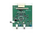
The ADC12D040 evaluation board comes fully assembled and ready for use. Refer to the Bill of Materials
for a description of components, to Figure 1 for major component placement and to Figure 2 for the
Evaluation Board schematic.
Figure 1. Component and Test Point Locations
3
Quick Start
Refer to Figure 1 for locations of test points and major components.
1. Connect a clean analog (not switching) +5V power source to Power Connector P1.
2. Set the output amplitude of the clock signal generator, if used, to 3 VP-P for the ADC12D040 or to 2VP-P
for the ADC12DL066 and the frequency to the desired sample rate.
3. Use R3 to set the reference voltage (VREF) at TP1 to +2.0V ±0.05 for the ADC12D040 or to 1.0V
±0.03V for the ADC12DL066. To use the ADC internal reference, verify a shorting jumper is placed on
JP2.
SNAU010A – December 2005 – Revised August 2014
Submit Documentation Feedback
ADC12D040, ADC11DL066, ADC12DL066 - A/D Converters with Internal
Reference and Sample & Hold
Copyright © 2005–2014, Texas Instruments Incorporated
3
�Functional Description
www.ti.com
4. Connect a signal source of 2.0 VP-P amplitude for the ADC12D040 or 1.0 VP-P for the ADC12DL066
from a suitable 50-Ω source (such as the Agilent 8644B synthesizer) to Analog Input BNC connector
J1. The ADC input signal can be observed at TP6.
Note: The signal to J1 should be applied through a bandpass filter to eliminate the noise and
harmonics commonly associated with signal sources. Even the best signal generators can not do
justice to a 12-bit ADC without such a filter. On the other hand, even a good bandpass filter will not
eliminate noise near its center frequency.
5. Put a jumper on JP5 to get an offset binary output from the ADC12D040. Remove any jumper from
JP5 for 2's complement output format.
6. Adjust the input signal amplitude as needed to ensure that the differential signal at TP6 is close to but
does not exceed 2.0VP-P for ADC12D040 or 1.0VP-P for ADC12DL066 from each side of TP6 to ground.
7. Check to be sure the correct frequency TTL oscillator is in socket U7, or apply an external 50-Ω, low
jitter, signal source to BNC J6. The amplitude of this signal should be between 2.5 and 3.3 VP-P. If using
an external source, remove the oscillator from U7. If using an oscillator at U7, remove the signal
source from J6. The presence of a second oscillator source could add noise to the conversion process.
Turn on the power.
8. The digitized signal is available at pins A4 through A18 and B4 through B15 of J5. See board
schematic of Figure 2.
9. Open the WaveVision 5 software
10. Select the WaveVision data format (Offset Binary or 2's Complement) from the Signal Sources Tab on
the right side of the screen.
11. The setup is now ready to capture data in the WaveVision 5 Software
4
Functional Description
Table 1 describes the function of the various jumpers on the ADC12D040 evaluation board. The
Evaluation Board schematic is shown in Figure 2.
Table 1. Jumper Functions
Jumper
4.1
Pins 1 & 2
JP1
Short pins 2-3 to select the on-board XO (U7) as the sampling clock source
Short pins 1-2 to select the signal source connected to J6 as the sampling clock source
JP2
Open to use external reference
Short to use on-chip reference
JP5
Short for offset binary output
Open for 2's complement
JP9
Should be hard-wired to short pins 1, 2, and 3 together
JP10
ADC12D040EVAL must have pins 1-2 shorted
ADC12DL066EVAL must have pins 2-3 shorted
JP11
Short pins 1-2 for output driver supply to be same as the ADC12D040 core supply.
Short pins 2-3 for 3.3V supply for the ADC12D040 output drivers. Hard- wired for ADC12DL066
Input (signal conditioning) Circuitry
The input signal to be digitized should be applied to BNC J1 for testing Channel A of the ADC or to BNC
J2 for testing Channel B.
The 50 Ω inputs J1 and J2 are intended to accept low-noise sine wave signals of 2.0 Volt peak-to-peak
amplitude for the ADC12D040 or 1.0 Volt peak-to-peak for the ADC12DL066. To accurately evaluate
dynamic performance, the input test signal will have to come from a high quality signal source (such as
the Agilent 8644B) and be passed through a high-quality bandpass filter with a 60 dB minimum stop band
attenuation. Even the best generators available do not provide a pure enough sine wave to properly
evaluate a high resolution ADC. Likewise, even with a good filter, apparent performance will still depend
upon the signal source used.
4
ADC12D040, ADC11DL066, ADC12DL066 - A/D Converters with Internal
Reference and Sample & Hold
SNAU010A – December 2005 – Revised August 2014
Submit Documentation Feedback
Copyright © 2005–2014, Texas Instruments Incorporated
�Functional Description
www.ti.com
Signal transformers T1 and T2 provide single-ended to differential conversion for the ADC12D040 inputs.
The common mode voltage at the ADC input comes from the reference voltage on the evaluation board
through R22 and R23.
Test points TP6 and TP5 may be used to observe the ADC input signals with differential probes. No scope
or other test equipment should be connected to TP6 or to TP5 while gathering data.
NOTE: If input frequency components above 50 MHz are required, remove capacitors C14 & C19
and C17 & C20 at the ADC differential input pins. These capacitors are located on the back
of the board.
4.2
ADC Reference Circuitry
These ADCs have an internal reference but can use an external reference as well. An adjustable
reference circuit is provided on this board. To use the external voltage reference, leave JP2 open. To use
the on-chip voltage reference, short the pins of JP2.
The evaluation board reference circuit will generate a reference voltage that can be adjusted within the
nominal range of 0.8 to 2.5 Volts for the ADC12D040 or 0.4 to 1.3 Volts for the ADC12DL066. The
ADC12D040 is will operate with VREF in the range of 1.0 to 2.2 Volts, with a nominal value of 2.0 Volts
while the ADC12DL066 is will operate with VREF in the range of 0.8 to 1.2 Volts, with a nominal value of
1.0 Volt. The external reference voltage can be monitored at test point TP1 and is set with R3.
ADC Clock Circuit
The crystal oscillator provided on the evaluation board is selected by shorting pins 2 and 3 of JP1. It is
best to remove any external signal generator when using this oscillator to reduce any unnecessary noise.
This board will also accept a clock signal from an external source by connecting that source to BNC J6
and shorting pins 1 and 2 of JP1. A very stable, low jitter source, such as the Agilent 8644B or equivalent,
should be used for the clock signal. An a.c. coupled circuit together with a d.c. biased resistive divider is
provided so the board can accept a 50 Ohm signal source in the range of 2.2 to 2.5VP-P to drive this input.
It is best to remove the oscillator at U7 when using an external clock source, or to remove the external
source when using U7, to reduce any unnecessary noise.
4.3
Digital Data Output
When using this evaluation board with a WaveVision 5 Data Capture Bboard, the 12-bit ADC12D040
output on both channels may be monitored at J3.
To cause the ADC outputs to be straight binary, pins 1-2 of JP5 should be shorted together. To cause the
ADC outputs to be 2’s Complement, no jumper should be placed on JP5.
4.4
Power Supply Connections
Power for the EVM should be supplied to connector P1 from a low-noise bench power supply. Switching
power supplies may add noise and degrade the performance of the ADC.
4.5
Power Requirements
Voltage and current requirements for the ADC12D040 Evaluation Board alone is +5V at 400 mA.
5
Software Operation and Settings
The latest version of the WaveVision 5 Software can be found online at www.ti.com.
SNAU010A – December 2005 – Revised August 2014
Submit Documentation Feedback
ADC12D040, ADC11DL066, ADC12DL066 - A/D Converters with Internal
Reference and Sample & Hold
Copyright © 2005–2014, Texas Instruments Incorporated
5
�Evaluation Board Specifications
Evaluation Board Specifications
Board Size:
Power Requirements:
Clock Frequency
Range:
Analog Input
Nominal Voltage:
5.9" x 6.18" (15.0 cm x 15.7 cm)
+5.0V, 340 mA
1.0 MHz to 40 MHz (ADC12D040)
1.0 MHz to 66 MHz (ADC12DL066)
2.0VP-P (ADC12D040)
1.0VP-P (ADC12DL066)
50 Ohms
Impedance:
Hardware Schematic
“C39”
1.5Ω
Ω
“C50”
1.5Ω
Ω
U1 pin 5
+5
U6E
74ACT04
OUTPUT CLOCK
10
R16
Open (51)
R91
Not Used
TP5
VINB
T2
C17
75pF
(47pF)
R10
Not
used
C20
75pF
(47pF)
VA
T4-6T
TP1
VREF
C7 C111
0.1uF 0.01uF
C13
0.1uF
C57
0.1uF
R88
Not Used
T1
R6
51
R9
Not
used
T4-6T
C48 0.1uF
C39
0.1uF
C47
0.1uF
C14
75pF
(47pF)
C19
75pF
(47pF)
C22
Not
used
2
+5A
C28
10uF
6.3V
C29
0.1uF
C23
10uF
6.3V
C24
0.1uF
B5
B4
B3
B2
B1
B0
B6
B7
B8
B9
B10
B11
ADC12D040
(ADC12DL066)
48
47
46
45
44
43
42
41
40
39
38
37
36
35
34
33
VD
RP3
16 A11
15 A10
14 A9
13 A8
12 A7
11 A6
10
9
B0
B1
B2
B3
B4
B5
OE VCC
Q1
D1
Q2
D2
Q3
D3
Q4
D4
Q5
D5
Q6
D6
Q7
D7
Q8
D8
GND CLK
C12
0.1uF
C10
0.1uF
2
1
1
2
3
4
5
6
7
8
TP3
OEA
1
2
JP5
OF
3
QB0
QB1
QB2
QB3
QB4
QB5
U9
LM1117MP-3.3
RP6
1
2
3
4
5
6
7
8
8 x 100
DIN 64
C3
0.1uF
JP9
A/B SEL
1
2
3
16
15
14
13
12
11
10
9
U3
A5
A4
A3
A2
A1
A0
1
2
3
4
5
6
7
8
9
10
A11
A10
A9
A8
A7
A6
OE VCC
Q1
D1
Q2
D2
Q3
D3
Q4
D4
Q5
D5
Q6
D6
Q7
D7
Q8
D8
GND CLK
2
+3P3V
1 OE VCC
2 D1
Q1
3 D2
Q2
4 D3
Q3
5 D4
Q4
6 D5
Q5
7 D6
Q6
8 D7
Q7
9 D8
Q8
10 GND CLK
A5
A4
A3
A2
A1
A0
L1 2.2nH
VD
VA
TP_GND_2
1 2 3
JP10
VA_SEL
RP7
20
19
18
17
16
15
14
13
12
11
JP11
VDR_SEL
L2
2.2nH
8 x 100
C2
0.1uF
J3
1
2
3
4
5
6
7
8
16
15
14
13
12
11
10
9
QB11
QB10
QB9
QB8
QB7
QB6
QB5
QB4
QB3
QB2
QB1
QB0
2
4
6
8
10
12
14
16
18
20
22
24
JP_CL
C21
0.1uF
1
8 x 100
2
3
4
OB[0..11]
A2
Vcc
A1
U8 WP
24C02
A0
GND
SCL
SDA
8
7
6
5
TP_GND_4
QB9
QA9
QB10
QA10
+5
R87
0
D6
C6
B6
A6
D5
C5
B5
A5
D4
C4
B4
A4
D3
C3
B3
A3
D2
C2
B2
A2
D1
C1
B1
A1
QB7
QA7
QB8
QA8
QB3
QA3
QB0
QA0
D18
C18
B18
A18
D17
C17
B17
A17
D16
C16
B16
A16
D15
C15
B15
A15
D14
C14
B14
A14
D13
C13
B13
A13
D24
C24
B24
A24
D23
C23
B23
A23
D22
C22
B22
A22
D21
C21
B21
A21
D20
C20
B20
A20
D19
C19
B19
A19
QB11
QA11
OA[0..11]
R90
0
J5
1
3
5
7
9
11
13
15
17
19
21
23
QA5
QA4
QA3
QA2
QA1
QA0
+5
TP_GND_3
QA11
QA10
QA9
QA8
QA7
QA6
QA5
QA4
QA3
QA2
QA1
QA0
RP8
20
19
18
17
16
15
14
13
12
11
74ACQ574 or
74ACT574
R92
5.1K
1 2 3
QA11
QA10
QA9
QA8
QA7
QA6
16
15
14
13
12
11
10
9
1
2
3
4
5
6
7
8
U2
VDR
TP_3.3
+V
R26
5.1K
74ACQ574 or
74ACT574
C18
10uF
6.3V
QB11
QB10
QB9
QB8
QB7
QB6
QB5
QB4
QB3
QB2
QB1
QB0
B1
B2
B3
B4
B5
B6
B7
B8
B9
B10
B11
B12
B13
B14
B15
B16
B17
B18
B19
B20
B21
B22
B23
B24
B25
B26
B27
B28
B29
B30
B31
B32
R25
5.1K
8 x 100
1
Values in
parentheses for
ADC12DL066
16
15
14
13
12
11
10
9
8 x 100
C4
0.1uF
20
19
18
17
16
15
14
13
12
11
74ACQ574 or
74ACT574
R46
5.1K
VA
D4
RED LED
TP_GND_1
QB6
QB7
QB8
QB9
QB10
QB11
RP2
VA
R85
5.1K
JP2
Int/EXT REF
R101
330
16
15
14
13
12
11
10
9
R97
5.1K
TP4
OEB
8 x 100
C58
0.1uF
1
2
3
4
5
6
7
8
U4
1
2
3
4
5
6
7
8
9
10
+5
λ
A1
A2
A3
A4
A5
A6
A7
A8
A9
A10
A11
A12
A13
A14
A15
A16
A17
A18
A19
A20
A21
A22
A23
A24
A25
A26
A27
A28
A29
A30
A31
A32
RP5
20
19
18
17
16
15
14
13
12
11
74ACQ574 or
74ACT574
8 x 100
1
2
3
4
5
6
7
8
OE VCC
Q1
D1
Q2
D2
Q3
D3
Q4
D4
Q5
D5
Q6
D6
Q7
D7
Q8
D8
GND CLK
+VDR
R19
5.1K
Z1 NFM41P11C204
1
3
2
U1
VD
DB5
DB4
DB3
DB2
DB1
DB0
OEB
DR GND
DA11
DA10
DA9
DA8
DA7
DA6
VD
QB4
QA4
2
D2
1
1N4001
POWER CONN
VINBVINB+
AGND
VRMB
VRPB
VRNB
VREF
AGND
VA
AGND
INT/EXT REF
VRNA
VRPA
VRMA
VINA+
VINA-
VA
Z3 NFM41P11C204
3
16
15
14
13
12
11
10
9
1
2
3
4
5
6
7
8
9
10
8 x 100
1
2
3
4
5
6
7
8
1
2
TP6
VINA
R12
51
R103
Not used
P1
1
2
3
4
5
6
7
8
9
10
11
12
13
14
15
16
+3.3A
R8
51
1
1
2
C55 0.1uF
C50 0.1uF
C49 0.1uF
C56 0.1uF
R23
200
C11
0.1uF
J1
VIN_A
R13
51
C8
0.1uF
B11
B10
B9
B8
B7
B6
RP2
C16
Not
used
QB2
QA2
R4
470
R22
200
VD
C63
0.1uF
C60
0.1uF
U5
16
15
14
13
12
11
10
9
D12
C12
B12
A12
D11
C11
B11
A11
D10
C10
B10
A10
D9
C9
B9
A9
D8
C8
B8
A8
D7
C7
B7
A7
R3
1K
D1
LM4040AIZ-2.5
(LM4041AIZ-1.2
for ADC11/12DL066)
VDR
R7
51
0.1uF
1
2
3
4
5
6
7
8
TP2
PD
C109
0.01uF
R11
51
R2
330
R96
5.1K
R86
Not used
VA
R102
Not used
C15
J2
VIN_B
C54
Not used
OB[0..11]
C9
0.1uF
R18
75
RP1
ADC CLOCK
OB[0..11]
J6
Ext_Clk
J4
+5V C5
0.1uF
LATCH CLOCK
U6B
74ACT04
CLK_SEL
READ CLOCK
R100
51
OB[0..11]
R100
Open
4
64
63
62
61
60
59
58
57
56
55
54
53
52
51
50
49
R17
150
3
R104
51
QB1
QA1
3
2
1
U6A
74ACT04
1
2
AGND
VA
VA
AGND
CLK
PD
DR GND
DB11
DB10
DB9
DB8
DB7
DB6
VDR
DR GND
DGND
C1
1uF
JP1
OA[0..11]
11
R21
Not used
+5
OA[0..11]
R20
51
U1 pin 12
Component substitution for ADC12DL066 only
READ_CLK
C6
0.1uF
AGND
VA
VA
AGND
OF
OEA
DR GND
DA0
DA1
DA2
DA3
DA4
DA5
VDR
DR GND
DGND
1 NC VCC 4
C48
1.0uF
C49
1.0uF
R98
51
(open)
U6D
74ACT04
9
8
C36
0.1uF
17
18
19
20
21
22
23
24
25
26
27
28
29
30
31
32
U7
40 MHz
(66 MHz)
2 GND OUT 3
U1 pin 13
U1 pin 6
QB5
QA5
7
QB6
QA6
6
www.ti.com
Future Bus Connector – 24 pin female
Figure 2. ADC12D040 / ADC12DL066 Evaluation Board Schematic
6
ADC12D040, ADC11DL066, ADC12DL066 - A/D Converters with Internal
Reference and Sample & Hold
SNAU010A – December 2005 – Revised August 2014
Submit Documentation Feedback
Copyright © 2005–2014, Texas Instruments Incorporated
�ADC12D040 / ADC12DL066 Evaluation Board Bill of Materials
www.ti.com
8
ADC12D040 / ADC12DL066 Evaluation Board Bill of Materials
Table 2. Bill of Materials
Qty
Reference
Part
1
C1
1uF
Size 0805
2
C109, C111
0.01uF
Size 0805
24
C2–C13, C15, C21, C24, C29,
C36, C47, C55–C58, C60, C63
0.1uF
Size 0805
4
C14, C17, C19, C20
75pF (ADC12D040)
47pF (ADC11/12DL066)
Size 0805
3
C18, C23, C28
10uF, 6.3V
Size 1206
–
C16, C22, C54
not populated
n/a
–
C25–C27, C30–C35, C40–C46,
C51–C53, C59, C61, C62
Not used
n/a
2
C39, C50
0.1uF (ADC12D040)
1.5Ω resistor (ADC11/12DL066)
Size 0805
2
C48, C49
0.1uF (ADC12D040)
1.0uF (ADC11/12DL066)
Size 0805
1
D1
LM4040AIZ-2.5 (ADC12D040)
LM4041AIZ-1.2 (ADC11/12DL066)
Texas Instruments
1
D2
1N4001 or 1N4002 or 1N4003
Various
1
D4
Red LED
Various
4
JP2, JP5, TP5, TP6
2-Pin Post Headers
DigiKey # A19351-ND
1
JP1
3-pin Post Headers
DigiKey # A19350-ND
1
JP9
Hard-Wired all together for ADC12D040
and ADC11/12DL066
1
JP11
3-pin Post Header for ADC12D040
Hard-Wired for ADC11/12DL066
DigiKey # A19350-ND
n/a
–
JP10
Hard wired
n/a
3
J1, J2, J6
BNC Connectors
DigiKey # ARF1177-ND
1
J3
24-pin Header
DigiKey # S2011-12-ND
-
J4
Not Populated
n/a
4
J5
Future Bus Connector
Amp # 223514-1
2
L1, L2
Wide-Band Choke
DigiKey # M2103-ND or JW Miller # FB20010-3B
1
P1
Terminal Block
DigiKey # ED1609-ND
1
R3
1K Pot
DigiKey # 3386P-102-ND
1
R90
0 Ohms
Size 1206
2
R2, R101
330, 5%
Size 1206
1
R4
470, 5%
Size 1206
10
R6–R8, R11–R13, R16, R20,
R100, R104
51, 5%
Size 1206
1
R18
75, 5%
Size 1206
1
R17
150, 5%
Size 1206
2
R22, R23
200, 5%
Size 1206
8
R19, R25, R26, R46, R85, R92,
R96, R97
5.1k, 5%
Size 1206
–
R9, R10, R21, R88, R86, R91,
R98, R102, R103
Not populated
n/a
–
R87
Not Populated
n/a
–
R1, R5
Not used
n/a
8
RP1–RP8
Resistor Pack - 8 x 100
DigiKey # 766-163-R101-ND or DigiKey # 768163-R101-ND
SNAU010A – December 2005 – Revised August 2014
Submit Documentation Feedback
ADC12D040, ADC11DL066, ADC12DL066 - A/D Converters with Internal
Reference and Sample & Hold
Copyright © 2005–2014, Texas Instruments Incorporated
7
�ADC12D040 / ADC12DL066 Evaluation Board Bill of Materials
www.ti.com
Table 2. Bill of Materials (continued)
1
TP–TP4, TP_GND_1,
TP_GND_2, TP_GND_3,
TP_GND_4, TP_3.3
Breakable Header
DigiKey # S1012-36-ND
2
T1, T2
Signal Transformer
MiniCircuits Type T4-6T
1
U1
ADC12D040CIVS, ADC11DL066CIVS or
ADC12DL066CIVS
Texas Instruments
4
U2, U3, U4, U5
74AT574SC or 74ACT574SC
Fairchild Semiconductor
1
U6
74AC04SC or 74ACT04SC
Fairchild Semiconductor
1
U7
40MHz Osc (ADC12D040)
66MHz Osc (ADC11/12DL066)
Pletronics #P1145-3SD-40.00M or
DigiKey # CTX120-ND (ADC12D040) or
Pletronics #P1145-3SD-66.667M or
DigiKey # CTX137-ND (ADC11/12L066)
1
U8
24C02
Various
1
U9
LM1117MP-3.3
Texas Instruments
2
Z1, Z3
Noise Filters
Murata # NFM41P11C204
1
--
4-Pin full-size oscillator socket
DigiKey # A462-ND
8
ADC12D040, ADC11DL066, ADC12DL066 - A/D Converters with Internal
Reference and Sample & Hold
SNAU010A – December 2005 – Revised August 2014
Submit Documentation Feedback
Copyright © 2005–2014, Texas Instruments Incorporated
�www.ti.com
Appendix A
A.1
Summary Tables of Test Points, Connectors, and Connectors
Table 3. Test Points on the ADC12D040/ADC11DL066/ADC12DL066 Evaluation Board
TP1: VREF
ADC Reference Voltage Test Point.
TP2: PD
Power Down control. Apply a logic high voltage here to power down the A/D Converter.
TP3: OEA
Output Enable for ADC "A". Apply a logic high voltage here to disable outputs "A".
TP4: OEB
Output Enable for ADC "B". Apply a logic high voltage here to disable outputs "B".
TP5: VINB
Differential input signal to ADC "B"
TP6: VINA
Differential input signal to ADC "A"
TP_3.3
3.3 Volt test point from the WaveVison4 Board.
TP_GND_1
Ground. Located in corner nearest TP_3.3
TP_GND_2
Ground. Located in corner nearest board identification silk screen.
TP_GND_3
Ground. Located in corner nearest Power Connector
TP_GND_4
Ground. Located in corner nearest BNC J2.
Connectors and Selection Jumpers on the ADC12D040/ADC11DL066/ADC12DL066 Evaluation
Board
J1: BNC Connector
Single-Ended input to ADC "A"
J2: BNC Connector
Single-Ended input to ADC "B"
J3: JP_CL
Put jumpers on all 12 pin pairs to make output bus available on J4 available for converter
selected by JP9.
J4: DIN 64
Not used.
J5: Future Bus connector
Future Bus connector for use with WaveVision 5 Data Capture Board
J6: BNC Connector
External Clock Input
SNAU010A – December 2005 – Revised August 2014
Submit Documentation Feedback
Copyright © 2005–2014, Texas Instruments Incorporated
9
�Summary Tables of Test Points, Connectors, and Connectors
www.ti.com
Table 4. Selection Jumpers on the ADC12D040/ADC11DL066/ADC12DL066 Evaluation Board
JP1: CLK_SEL
Jumper pins 2-3 to select on-board oscillator at U7 or jumper pins 1-2 to select external clock at J6
JP2: INT/EXT REF
Place jumper on these pins to select the internal 1.0V reference; leave jumper off to use external reference.
JP3:
Not Used
JP4:
Not Used
JP5: OF
Place jumper on these pins to select Offset Binary output format; leave jumper off for 2's complement.
JP6:
Not Used
JP7:
Not Used
JP8:
Not Used
JP9: A/B SEL
Hard-wired together
JP10: VA_SEL
Hard-wired to +5.0V for ADC12D040. Hard-wired to 3.3V for ADC12DL066
JP11: VDR_SEL
Jumper pins 2-3 to select 3.3V for VDR (output driver supply) or jumper pins 1-2 to select ADC supply for VDR.
Hard-wired to 3.3V for ADC12DL066
Table 5. P1: Connector - Power Supply Connections
P1-1
+5V
Positive Supply voltage (+5V)
P1-2
GND
Power Supply Ground
Table 6. J3: Latch Outputs
10
J3 pin number
Signal (when channel enabled)
1, 2
B11(MSB) Ch A, B11(MSB) Ch B
3, 4
B10 Ch A, B10 Ch B
5, 6
B9 Ch A, B9 Ch B
7, 8
B8 Ch A, B8 Ch B
9, 10
B7 Ch A, B7 Ch B
11, 12
B6 Ch A, B6 Ch B
13, 14
B5 Ch A, B5 Ch B
15, 16
B4 Ch A, B4 Ch B
17, 18
B3 Ch A, B3 Ch B
19, 20
B2 Ch A, B2 Ch B
21, 22
B1 Ch A, B1 Ch B
23, 24
B0(LSB) Ch A, B0(LSB)
SNAU010A – December 2005 – Revised August 2014
Submit Documentation Feedback
Copyright © 2005–2014, Texas Instruments Incorporated
�Summary Tables of Test Points, Connectors, and Connectors
www.ti.com
Table 7. J5: Future Bus connector for use with WAVEVSN BRD 4.0 Data Capture Board
J5 Pin Number
Signal
A1, B1, A2, B2
Not connected
C1 thru C24
Ground
A3, A22, B3, D1, D16
Ground
D2
READ_CLK to clock data into RAM
A4
QA11 - Bit 11 (MSB) output for ADC "A"
B4
QB11 - Bit 11 output for ADC "B"
A5
QA10 - Bit 10 output for ADC "A"
B5
QB10 - Bit 10 output for ADC "B"
A6
QA9 - Bit 9 output for ADC "A"
B6
QB9 - Bit 9 output for ADC "B"
A7
QA8 - Bit 8 output for ADC "A"
B7
QB8 - Bit 8 output for ADC "B"
A8
QA7 - Bit 7 output for ADC "A"
B8
QB7 - Bit 7 output for ADC "B"
A9
QA6 - Bit 7 output for ADC "A"
B9
QB6 - Bit 7 output for ADC "B"
A10
QA5 - Bit 7 output for ADC "A"
B10
QB5 - Bit 7 output for ADC "B"
A11
QA4 - Bit 7 output for ADC "A"
B11
QB4 - Bit 7 output for ADC "B"
A12
QA3 - Bit 7 output for ADC "A"
B12
QB3 - Bit 7 output for ADC "B"
A13
QA2 - Bit 7 output for ADC "A"
B13
QB2 - Bit 7 output for ADC "B"
A14
QA1 - Bit 7 output for ADC "A"
B14
QB1 - Bit 7 output for ADC "B"
A15
QA0 - Bit 7 output for ADC "A"
B15
QB0 - Bit 7 output for ADC "B"
D4, D6, D8
Board ID pins - not used
A23, B23, A24, B24
3.3V from WaveVision4 Data Capture Board
A16 thru A21
Not Used
B16 thru B21
Not Used
D5, D7, D9 thru D15
Not Used
D17 thru D24
Not Used
SNAU010A – December 2005 – Revised August 2014
Submit Documentation Feedback
Copyright © 2005–2014, Texas Instruments Incorporated
11
�Revision History
www.ti.com
Revision History
Changes from Original (December 2005) to A Revision ................................................................................................ Page
•
•
•
Changed the document to the TI format ............................................................................................... 1
Changed From: "WaveVision4 software" To: "WaveVision5 software" in the Introduction ..................................... 2
Changed Table 2 .......................................................................................................................... 7
NOTE: Page numbers for previous revisions may differ from page numbers in the current version.
12
Revision History
SNAU010A – December 2005 – Revised August 2014
Submit Documentation Feedback
Copyright © 2005–2014, Texas Instruments Incorporated
�ADDITIONAL TERMS AND CONDITIONS, WARNINGS, RESTRICTIONS, AND DISCLAIMERS FOR
EVALUATION MODULES
Texas Instruments Incorporated (TI) markets, sells, and loans all evaluation boards, kits, and/or modules (EVMs) pursuant to, and user
expressly acknowledges, represents, and agrees, and takes sole responsibility and risk with respect to, the following:
1.
User agrees and acknowledges that EVMs are intended to be handled and used for feasibility evaluation only in laboratory and/or
development environments. Notwithstanding the foregoing, in certain instances, TI makes certain EVMs available to users that do not
handle and use EVMs solely for feasibility evaluation only in laboratory and/or development environments, but may use EVMs in a
hobbyist environment. All EVMs made available to hobbyist users are FCC certified, as applicable. Hobbyist users acknowledge, agree,
and shall comply with all applicable terms, conditions, warnings, and restrictions in this document and are subject to the disclaimer and
indemnity provisions included in this document.
2. Unless otherwise indicated, EVMs are not finished products and not intended for consumer use. EVMs are intended solely for use by
technically qualified electronics experts who are familiar with the dangers and application risks associated with handling electrical
mechanical components, systems, and subsystems.
3. User agrees that EVMs shall not be used as, or incorporated into, all or any part of a finished product.
4. User agrees and acknowledges that certain EVMs may not be designed or manufactured by TI.
5. User must read the user's guide and all other documentation accompanying EVMs, including without limitation any warning or
restriction notices, prior to handling and/or using EVMs. Such notices contain important safety information related to, for example,
temperatures and voltages. For additional information on TI's environmental and/or safety programs, please visit www.ti.com/esh or
contact TI.
6. User assumes all responsibility, obligation, and any corresponding liability for proper and safe handling and use of EVMs.
7. Should any EVM not meet the specifications indicated in the user’s guide or other documentation accompanying such EVM, the EVM
may be returned to TI within 30 days from the date of delivery for a full refund. THE FOREGOING LIMITED WARRANTY IS THE
EXCLUSIVE WARRANTY MADE BY TI TO USER AND IS IN LIEU OF ALL OTHER WARRANTIES, EXPRESSED, IMPLIED, OR
STATUTORY, INCLUDING ANY WARRANTY OF MERCHANTABILITY OR FITNESS FOR ANY PARTICULAR PURPOSE. TI SHALL
NOT BE LIABLE TO USER FOR ANY INDIRECT, SPECIAL, INCIDENTAL, OR CONSEQUENTIAL DAMAGES RELATED TO THE
HANDLING OR USE OF ANY EVM.
8. No license is granted under any patent right or other intellectual property right of TI covering or relating to any machine, process, or
combination in which EVMs might be or are used. TI currently deals with a variety of customers, and therefore TI’s arrangement with
the user is not exclusive. TI assumes no liability for applications assistance, customer product design, software performance, or
infringement of patents or services with respect to the handling or use of EVMs.
9. User assumes sole responsibility to determine whether EVMs may be subject to any applicable federal, state, or local laws and
regulatory requirements (including but not limited to U.S. Food and Drug Administration regulations, if applicable) related to its handling
and use of EVMs and, if applicable, compliance in all respects with such laws and regulations.
10. User has sole responsibility to ensure the safety of any activities to be conducted by it and its employees, affiliates, contractors or
designees, with respect to handling and using EVMs. Further, user is responsible to ensure that any interfaces (electronic and/or
mechanical) between EVMs and any human body are designed with suitable isolation and means to safely limit accessible leakage
currents to minimize the risk of electrical shock hazard.
11. User shall employ reasonable safeguards to ensure that user’s use of EVMs will not result in any property damage, injury or death,
even if EVMs should fail to perform as described or expected.
12. User shall be solely responsible for proper disposal and recycling of EVMs consistent with all applicable federal, state, and local
requirements.
Certain Instructions. User shall operate EVMs within TI’s recommended specifications and environmental considerations per the user’s
guide, accompanying documentation, and any other applicable requirements. Exceeding the specified ratings (including but not limited to
input and output voltage, current, power, and environmental ranges) for EVMs may cause property damage, personal injury or death. If
there are questions concerning these ratings, user should contact a TI field representative prior to connecting interface electronics including
input power and intended loads. Any loads applied outside of the specified output range may result in unintended and/or inaccurate
operation and/or possible permanent damage to the EVM and/or interface electronics. Please consult the applicable EVM user's guide prior
to connecting any load to the EVM output. If there is uncertainty as to the load specification, please contact a TI field representative. During
normal operation, some circuit components may have case temperatures greater than 60°C as long as the input and output are maintained
at a normal ambient operating temperature. These components include but are not limited to linear regulators, switching transistors, pass
transistors, and current sense resistors which can be identified using EVMs’ schematics located in the applicable EVM user's guide. When
placing measurement probes near EVMs during normal operation, please be aware that EVMs may become very warm. As with all
electronic evaluation tools, only qualified personnel knowledgeable in electronic measurement and diagnostics normally found in
development environments should use EVMs.
Agreement to Defend, Indemnify and Hold Harmless. User agrees to defend, indemnify, and hold TI, its directors, officers, employees,
agents, representatives, affiliates, licensors and their representatives harmless from and against any and all claims, damages, losses,
expenses, costs and liabilities (collectively, "Claims") arising out of, or in connection with, any handling and/or use of EVMs. User’s
indemnity shall apply whether Claims arise under law of tort or contract or any other legal theory, and even if EVMs fail to perform as
described or expected.
Safety-Critical or Life-Critical Applications. If user intends to use EVMs in evaluations of safety critical applications (such as life support),
and a failure of a TI product considered for purchase by user for use in user’s product would reasonably be expected to cause severe
personal injury or death such as devices which are classified as FDA Class III or similar classification, then user must specifically notify TI
of such intent and enter into a separate Assurance and Indemnity Agreement.
�RADIO FREQUENCY REGULATORY COMPLIANCE INFORMATION FOR EVALUATION MODULES
Texas Instruments Incorporated (TI) evaluation boards, kits, and/or modules (EVMs) and/or accompanying hardware that is marketed, sold,
or loaned to users may or may not be subject to radio frequency regulations in specific countries.
General Statement for EVMs Not Including a Radio
For EVMs not including a radio and not subject to the U.S. Federal Communications Commission (FCC) or Industry Canada (IC)
regulations, TI intends EVMs to be used only for engineering development, demonstration, or evaluation purposes. EVMs are not finished
products typically fit for general consumer use. EVMs may nonetheless generate, use, or radiate radio frequency energy, but have not been
tested for compliance with the limits of computing devices pursuant to part 15 of FCC or the ICES-003 rules. Operation of such EVMs may
cause interference with radio communications, in which case the user at his own expense will be required to take whatever measures may
be required to correct this interference.
General Statement for EVMs including a radio
User Power/Frequency Use Obligations: For EVMs including a radio, the radio included in such EVMs is intended for development and/or
professional use only in legally allocated frequency and power limits. Any use of radio frequencies and/or power availability in such EVMs
and their development application(s) must comply with local laws governing radio spectrum allocation and power limits for such EVMs. It is
the user’s sole responsibility to only operate this radio in legally acceptable frequency space and within legally mandated power limitations.
Any exceptions to this are strictly prohibited and unauthorized by TI unless user has obtained appropriate experimental and/or development
licenses from local regulatory authorities, which is the sole responsibility of the user, including its acceptable authorization.
U.S. Federal Communications Commission Compliance
For EVMs Annotated as FCC – FEDERAL COMMUNICATIONS COMMISSION Part 15 Compliant
Caution
This device complies with part 15 of the FCC Rules. Operation is subject to the following two conditions: (1) This device may not cause
harmful interference, and (2) this device must accept any interference received, including interference that may cause undesired operation.
Changes or modifications could void the user's authority to operate the equipment.
FCC Interference Statement for Class A EVM devices
This equipment has been tested and found to comply with the limits for a Class A digital device, pursuant to part 15 of the FCC Rules.
These limits are designed to provide reasonable protection against harmful interference when the equipment is operated in a commercial
environment. This equipment generates, uses, and can radiate radio frequency energy and, if not installed and used in accordance with the
instruction manual, may cause harmful interference to radio communications. Operation of this equipment in a residential area is likely to
cause harmful interference in which case the user will be required to correct the interference at its own expense.
FCC Interference Statement for Class B EVM devices
This equipment has been tested and found to comply with the limits for a Class B digital device, pursuant to part 15 of the FCC Rules.
These limits are designed to provide reasonable protection against harmful interference in a residential installation. This equipment
generates, uses and can radiate radio frequency energy and, if not installed and used in accordance with the instructions, may cause
harmful interference to radio communications. However, there is no guarantee that interference will not occur in a particular installation. If
this equipment does cause harmful interference to radio or television reception, which can be determined by turning the equipment off and
on, the user is encouraged to try to correct the interference by one or more of the following measures:
• Reorient or relocate the receiving antenna.
• Increase the separation between the equipment and receiver.
• Connect the equipment into an outlet on a circuit different from that to which the receiver is connected.
• Consult the dealer or an experienced radio/TV technician for help.
Industry Canada Compliance (English)
For EVMs Annotated as IC – INDUSTRY CANADA Compliant:
This Class A or B digital apparatus complies with Canadian ICES-003.
Changes or modifications not expressly approved by the party responsible for compliance could void the user’s authority to operate the
equipment.
Concerning EVMs Including Radio Transmitters
This device complies with Industry Canada licence-exempt RSS standard(s). Operation is subject to the following two conditions: (1) this
device may not cause interference, and (2) this device must accept any interference, including interference that may cause undesired
operation of the device.
Concerning EVMs Including Detachable Antennas
Under Industry Canada regulations, this radio transmitter may only operate using an antenna of a type and maximum (or lesser) gain
approved for the transmitter by Industry Canada. To reduce potential radio interference to other users, the antenna type and its gain should
be so chosen that the equivalent isotropically radiated power (e.i.r.p.) is not more than that necessary for successful communication.
This radio transmitter has been approved by Industry Canada to operate with the antenna types listed in the user guide with the maximum
permissible gain and required antenna impedance for each antenna type indicated. Antenna types not included in this list, having a gain
greater than the maximum gain indicated for that type, are strictly prohibited for use with this device.
�Canada Industry Canada Compliance (French)
Cet appareil numérique de la classe A ou B est conforme à la norme NMB-003 du Canada
Les changements ou les modifications pas expressément approuvés par la partie responsable de la conformité ont pu vider l’autorité de
l'utilisateur pour actionner l'équipement.
Concernant les EVMs avec appareils radio
Le présent appareil est conforme aux CNR d'Industrie Canada applicables aux appareils radio exempts de licence. L'exploitation est
autorisée aux deux conditions suivantes : (1) l'appareil ne doit pas produire de brouillage, et (2) l'utilisateur de l'appareil doit accepter tout
brouillage radioélectrique subi, même si le brouillage est susceptible d'en compromettre le fonctionnement.
Concernant les EVMs avec antennes détachables
Conformément à la réglementation d'Industrie Canada, le présent émetteur radio peut fonctionner avec une antenne d'un type et d'un gain
maximal (ou inférieur) approuvé pour l'émetteur par Industrie Canada. Dans le but de réduire les risques de brouillage radioélectrique à
l'intention des autres utilisateurs, il faut choisir le type d'antenne et son gain de sorte que la puissance isotrope rayonnée équivalente
(p.i.r.e.) ne dépasse pas l'intensité nécessaire à l'établissement d'une communication satisfaisante.
Le présent émetteur radio a été approuvé par Industrie Canada pour fonctionner avec les types d'antenne énumérés dans le manuel
d’usage et ayant un gain admissible maximal et l'impédance requise pour chaque type d'antenne. Les types d'antenne non inclus dans
cette liste, ou dont le gain est supérieur au gain maximal indiqué, sont strictement interdits pour l'exploitation de l'émetteur.
Mailing Address: Texas Instruments, Post Office Box 655303, Dallas, Texas 75265
Copyright © 2014, Texas Instruments Incorporated
spacer
Important Notice for Users of EVMs Considered “Radio Frequency Products” in Japan
EVMs entering Japan are NOT certified by TI as conforming to Technical Regulations of Radio Law of Japan.
If user uses EVMs in Japan, user is required by Radio Law of Japan to follow the instructions below with respect to EVMs:
1.
2.
3.
Use EVMs in a shielded room or any other test facility as defined in the notification #173 issued by Ministry of Internal Affairs and
Communications on March 28, 2006, based on Sub-section 1.1 of Article 6 of the Ministry’s Rule for Enforcement of Radio Law of
Japan,
Use EVMs only after user obtains the license of Test Radio Station as provided in Radio Law of Japan with respect to EVMs, or
Use of EVMs only after user obtains the Technical Regulations Conformity Certification as provided in Radio Law of Japan with respect
to EVMs. Also, do not transfer EVMs, unless user gives the same notice above to the transferee. Please note that if user does not
follow the instructions above, user will be subject to penalties of Radio Law of Japan.
http://www.tij.co.jp
【無線電波を送信する製品の開発キットをお使いになる際の注意事項】 本開発キットは技術基準適合証明を受けておりません。 本製品の
ご使用に際しては、電波法遵守のため、以下のいずれかの措置を取っていただく必要がありますのでご注意ください。
1.
2.
3.
電波法施行規則第6条第1項第1号に基づく平成18年3月28日総務省告示第173号で定められた電波暗室等の試験設備でご使用いただく。
実験局の免許を取得後ご使用いただく。
技術基準適合証明を取得後ご使用いただく。。
なお、本製品は、上記の「ご使用にあたっての注意」を譲渡先、移転先に通知しない限り、譲渡、移転できないものとします
上記を遵守頂けない場合は、電波法の罰則が適用される可能性があることをご留意ください。
日本テキサス・インスツルメンツ株式会社
東京都新宿区西新宿6丁目24番1号
西新宿三井ビル
http://www.tij.co.jp
Texas Instruments Japan Limited
(address) 24-1, Nishi-Shinjuku 6 chome, Shinjuku-ku, Tokyo, Japan
�IMPORTANT NOTICE
Texas Instruments Incorporated and its subsidiaries (TI) reserve the right to make corrections, enhancements, improvements and other
changes to its semiconductor products and services per JESD46, latest issue, and to discontinue any product or service per JESD48, latest
issue. Buyers should obtain the latest relevant information before placing orders and should verify that such information is current and
complete. All semiconductor products (also referred to herein as “components”) are sold subject to TI’s terms and conditions of sale
supplied at the time of order acknowledgment.
TI warrants performance of its components to the specifications applicable at the time of sale, in accordance with the warranty in TI’s terms
and conditions of sale of semiconductor products. Testing and other quality control techniques are used to the extent TI deems necessary
to support this warranty. Except where mandated by applicable law, testing of all parameters of each component is not necessarily
performed.
TI assumes no liability for applications assistance or the design of Buyers’ products. Buyers are responsible for their products and
applications using TI components. To minimize the risks associated with Buyers’ products and applications, Buyers should provide
adequate design and operating safeguards.
TI does not warrant or represent that any license, either express or implied, is granted under any patent right, copyright, mask work right, or
other intellectual property right relating to any combination, machine, or process in which TI components or services are used. Information
published by TI regarding third-party products or services does not constitute a license to use such products or services or a warranty or
endorsement thereof. Use of such information may require a license from a third party under the patents or other intellectual property of the
third party, or a license from TI under the patents or other intellectual property of TI.
Reproduction of significant portions of TI information in TI data books or data sheets is permissible only if reproduction is without alteration
and is accompanied by all associated warranties, conditions, limitations, and notices. TI is not responsible or liable for such altered
documentation. Information of third parties may be subject to additional restrictions.
Resale of TI components or services with statements different from or beyond the parameters stated by TI for that component or service
voids all express and any implied warranties for the associated TI component or service and is an unfair and deceptive business practice.
TI is not responsible or liable for any such statements.
Buyer acknowledges and agrees that it is solely responsible for compliance with all legal, regulatory and safety-related requirements
concerning its products, and any use of TI components in its applications, notwithstanding any applications-related information or support
that may be provided by TI. Buyer represents and agrees that it has all the necessary expertise to create and implement safeguards which
anticipate dangerous consequences of failures, monitor failures and their consequences, lessen the likelihood of failures that might cause
harm and take appropriate remedial actions. Buyer will fully indemnify TI and its representatives against any damages arising out of the use
of any TI components in safety-critical applications.
In some cases, TI components may be promoted specifically to facilitate safety-related applications. With such components, TI’s goal is to
help enable customers to design and create their own end-product solutions that meet applicable functional safety standards and
requirements. Nonetheless, such components are subject to these terms.
No TI components are authorized for use in FDA Class III (or similar life-critical medical equipment) unless authorized officers of the parties
have executed a special agreement specifically governing such use.
Only those TI components which TI has specifically designated as military grade or “enhanced plastic” are designed and intended for use in
military/aerospace applications or environments. Buyer acknowledges and agrees that any military or aerospace use of TI components
which have not been so designated is solely at the Buyer's risk, and that Buyer is solely responsible for compliance with all legal and
regulatory requirements in connection with such use.
TI has specifically designated certain components as meeting ISO/TS16949 requirements, mainly for automotive use. In any case of use of
non-designated products, TI will not be responsible for any failure to meet ISO/TS16949.
Products
Applications
Audio
www.ti.com/audio
Automotive and Transportation
www.ti.com/automotive
Amplifiers
amplifier.ti.com
Communications and Telecom
www.ti.com/communications
Data Converters
dataconverter.ti.com
Computers and Peripherals
www.ti.com/computers
DLP® Products
www.dlp.com
Consumer Electronics
www.ti.com/consumer-apps
DSP
dsp.ti.com
Energy and Lighting
www.ti.com/energy
Clocks and Timers
www.ti.com/clocks
Industrial
www.ti.com/industrial
Interface
interface.ti.com
Medical
www.ti.com/medical
Logic
logic.ti.com
Security
www.ti.com/security
Power Mgmt
power.ti.com
Space, Avionics and Defense
www.ti.com/space-avionics-defense
Microcontrollers
microcontroller.ti.com
Video and Imaging
www.ti.com/video
RFID
www.ti-rfid.com
OMAP Applications Processors
www.ti.com/omap
TI E2E Community
e2e.ti.com
Wireless Connectivity
www.ti.com/wirelessconnectivity
Mailing Address: Texas Instruments, Post Office Box 655303, Dallas, Texas 75265
Copyright © 2014, Texas Instruments Incorporated
�