ADC14155
www.ti.com
SNAS350I – APRIL 2006 – REVISED APRIL 2013
ADC14155 14-Bit, 155 MSPS, 1.1 GHz Bandwidth A/D Converter
Check for Samples: ADC14155
FEATURES
DESCRIPTION
•
•
•
•
•
•
•
•
The ADC14155 is a high-performance CMOS analogto-digital converter capable of converting analog input
signals into 14-bit digital words at rates up to 155
Mega Samples Per Second (MSPS). This converter
uses a differential, pipelined architecture with digital
error correction and an on-chip sample-and-hold
circuit to minimize power consumption and the
external component count, while providing excellent
dynamic performance. A unique sample-and-hold
stage yields a full-power bandwidth of 1.1 GHz. The
ADC14155 operates from dual +3.3V and +1.8V
power supplies and consumes 967 mW of power at
155 MSPS.
1
2
•
•
•
1.1 GHz Full Power Bandwidth
Internal Sample-and-Hold Circuit
Low Power Consumption
Internal Precision 1.0V Reference
Single-Ended or Differential Clock Modes
Data Ready Output Clock
Clock Duty Cycle Stabilizer
Dual +3.3V and +1.8V Supply Operation
(+/- 10%)
Power-Down Mode
Offset Binary or 2's Complement Output Data
Format
48-pin WQFN Package, (7x7x0.8mm, 0.5mm
Pin-Pitch)
APPLICATIONS
•
•
•
•
•
•
•
High IF Sampling Receivers
Wireless Base Station Receivers
Power Amplifier Linearization
Multi-carrier, Multi-mode Receivers
Test and Measurement Equipment
Communications Instrumentation
Radar Systems
KEY SPECIFICATIONS
•
•
•
•
•
•
•
Resolution: 14 Bits
Conversion Rate: 155 MSPS
SNR (fIN = 70 MHz): 71.3 dBFS (typ)
SFDR (fIN = 70 MHz): 87.0 dBFS (typ)
ENOB (fIN = 70 MHz): 11.5 bits (typ)
Full Power Bandwidth: 1.1 GHz (typ)
Power Consumption: 967 mW (typ)
The separate +1.8V supply for the digital output
interface allows lower power operation with reduced
noise. A power-down feature reduces the power
consumption to 5 mW with the clock input disabled,
while still allowing fast wake-up time to full operation.
The differential inputs provide a full scale differential
input swing equal to 2 times the reference voltage. A
stable 1.0V internal voltage reference is provided, or
the ADC14155 can be operated with an external
reference.
The ADC14155 can be configured for either singleended or differential operation. Clock mode
(differential versus single-ended) and output data
format (offset binary versus 2's complement) are pinselectable. A duty cycle stabilizer maintains
performance over a wide range of clock duty cycles.
The ADC14155 is available in a 48-lead WQFN
package and operates over the industrial temperature
range of −40°C to +85°C.
1
2
Please be aware that an important notice concerning availability, standard warranty, and use in critical applications of
Texas Instruments semiconductor products and disclaimers thereto appears at the end of this data sheet.
All trademarks are the property of their respective owners.
PRODUCTION DATA information is current as of publication date.
Products conform to specifications per the terms of the Texas
Instruments standard warranty. Production processing does not
necessarily include testing of all parameters.
Copyright © 2006–2013, Texas Instruments Incorporated
�ADC14155
SNAS350I – APRIL 2006 – REVISED APRIL 2013
www.ti.com
Block Diagram
INTERNAL
REFERENCE
VREF
VRP
VRM
VRN
14
VIN+
VIN-
14BIT HIGH SPEED
PIPELINE ADC
SHA
D0 - D13
DIGITAL
CORRECTION
OVR
DRDY
CLK+
CLK-
CLOCK/DUTY CYCLE
STABILIZER
AGND
AGND
VA
VA
37
38
39
AGND
VRP
VRN
VA
40
41
42
43
VRM
44
AGND
VREF
45
46
7
8
30
29
9
28
10
27
11
26
DRGND
DRDY
OVR
D13 (MSB)
D12
D11
D10
D9
D8
DRGND
VDR
24
25
VDR
D7
23
D6
22
D5
20
21
D4
VD
D3
12
19
* Exposed pad must be soldered to ground
plane to ensure rated performance.
13
CLK-
31
ADC14155
(Top View)
D2
CLK+
6
18
AGND
32
D1
VA
5
17
CLK_SEL/DF
33
(LSB) D0
PD
4
16
VA
34
DRGND
AGND
3
15
VIN+
35
VDR
VIN-
36
2
DGND
AGND
1
14
VA
47
48
VA
Connection Diagram
Figure 1. 48-Lead WQFN Package
Package Number RHS0048A
2
Submit Documentation Feedback
Copyright © 2006–2013, Texas Instruments Incorporated
Product Folder Links: ADC14155
�ADC14155
www.ti.com
SNAS350I – APRIL 2006 – REVISED APRIL 2013
PIN DESCRIPTIONS AND EQUIVALENT CIRCUITS
Pin No.
Symbol
Equivalent Circuit
Description
ANALOG I/O
3
VIN−
Differential analog input pins. The differential full-scale input signal
level is two times the reference voltage with each input pin signal
centered on a common mode voltage, VCM.
VA
4
VIN+
AGND
43
VRP
45
VRM
VA
VRM
VA
VRN
VREF
44
VRN
VA
VRP
These pins should each be bypassed to AGND with a low ESL
(equivalent series inductance) 0.1 µF capacitor placed very close to
the pin to minimize stray inductance. A 0.1 µF capacitor should be
placed between VRP and VRN as close to the pins as possible, and a
10 µF capacitor should be placed in parallel.
VRP and VRN should not be loaded. VRM may be loaded to 1mA for
use as a temperature stable 1.5V reference.
It is recommended to use VRM to provide the common mode voltage,
VCM, for the differential analog inputs, VIN+ and VIN−.
AGND
VA
IDC
46
VREF
AGND
This pin can be used as either the +1.0V internal reference voltage
output (internal reference operation) or as the external reference
voltage input (external reference operation).
To use the internal reference, VREF should be decoupled to AGND
with a 0.1 µF, low equivalent series inductance (ESL) capacitor. In
this mode, VREF defaults as the output for the internal 1.0V
reference.
To use an external reference, overdrive this pin with a low noise
external reference voltage. The output impedance of the internal
reference at this pin is 9kΩ. Therefore, to overdrive this pin, the
impedance of the external reference source should be
很抱歉,暂时无法提供与“ADC14155CISQ/NOPB”相匹配的价格&库存,您可以联系我们找货
免费人工找货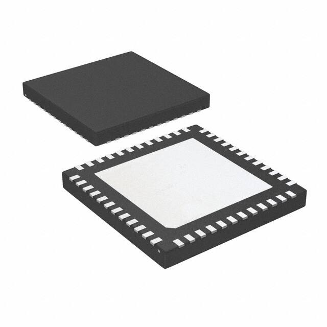


 工商网监
湘ICP备2023018690号
工商网监
湘ICP备2023018690号
