Evaluation Board User’s Guide for
ADC14155W-MLS:
14-Bit, 155 MSPS Analog to Digital Converter
www.national.com
Rev 1.2
May 2011
�ADC14155W-MLS Evaluation Board User’s Guide
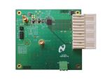
Analog Input
FIN > 150 MHz
Analog Input
FIN < 150 MHz
Analog Input
Network
ADC
PD
Jumper
CLK_SEL/DF
Jumper
PLD
MODE
Jumper
INV
Jumper
FutureBus
Connector
SingleEnded
Clock
Input
5.0 V Power
Connector
Figure 1. ADC14155 Evaluation Board and jumper locactions.
The board shown is the ADC14155LCVAL, with the analog input network configured for opmtimum performance
when input frequency is less than 150 MHz. The high speed board, ADC14155HCVAL, has a different analog input
network, optimized for input frequencies greater than 150 MHz.
-2-
www.national.com
Rev 1.2
�ADC14155W-MLS Evaluation Board User’s Guide
1.0 Introduction
3.0 Quick Start
The ADC14155 Evaluation Board is designed to
support the ADC14155W-MLS 14-bit 155 Mega
Sample Per Second (MSPS) Analog to Digital
Converter.
The ADC14155 evaluation board enables easy set up
for evaluating the performance of the ADC14155.
The ADC14155 Evaluation Board comes in two
versions:
1. ADC14155HCVAL (high frequency version)
for input frequencies greater than 150 MHz.
2. ADC14155LCVAL (low frequency version)
for input frequencies less than 150 MHz.
The digital data from the ADC14155 evaluation board
can be captured with a suitable instrument, such as a
logic analyzer, or with National Semiconductor’s
WaveVision 5 data acquisition hardware and software
platform. The ADC14155 evaluation board can be
connected to the data acquisition hardware through the
FutureBus connector (schematic reference designator
FB).
The ADC14155 evaluation board is compatible with
National Semiconductor’s WaveVision 5 Digital
Interface Board and WaveVision software. Please note
that the ADC14155 evaluation board is not compatible
with the WaveVision 4.x Digital Interface Boards.
The WaveVision hardware and software package
allows fast and easy data acquisition and analysis. The
WaveVision hardware connects to a host PC via a USB
cable and is fully configured and controlled by the latest
WaveVision software. The latest WaveVision software
is provided with the ADC14155 evaluation kit. The
WaveVision data acquisition hardware is available
through
the
National
Semiconductor
website
(http://www.national.com/appinfo/adc/).
2.0 Board Assembly
Each evaluation board from the factory is configured for
single-ended clock operation and is populated with an
analog input network which has been optimized for one
of two analog input frequencies ranges:
1. ADC14155HCVAL (high frequency version)
for input frequencies greater than 150 MHz.
If the WaveVision data acquisition and data analysis
system is to be used for capturing data, please follow
the Quick Start Guide in the WaveVision User’s Guide
to install the required software and to connect the
WaveVision Digital Interface Board to the PC. Please
note that the ADC14155 evaluation board is only
compatible with National Semiconductor’s WaveVision
5 Digital Interface boards.
3.1 Evaluation Board Jumper Positions
The ADC14155 evaluation board jumpers should be
configured as follows. Please refer to Figure 1 for the
exact jumper locations.
1. J1 solder jumper on the reverse of the board
should be shorted.
2. The MODE solder jumper on the front of the board
should be shorted and the INV solder jumper
should be left open. See Section 4.4 for more
detailed information regarding the function of the
MODE and INV jumpers.
3. The PD pin jumper places the ADC14155 into
either power-down or sleep mode. Table 1 below
shows how to select between the power-down
modes.
PD Jumper
Setting
Open
1-2
3-4
Mode
Normal Operation
Power-down
Sleep
Table 1. PD/Sleep Selection Table
4. CLK_SEL/DF pin jumpers select the output data
format (2’s complement or offset binary) and clock
mode (single-ended or differential). Table 2 below
shows how to select between the clock modes and
output data formats.
Please note that the
ADC14155 evaluation board is delivered with the
ADC14155 clock input configured for single-ended
operation and Offset Binary output data format
(Jumper 7-8).
CLK_SEL/DF
Jumper
Setting
1-2
3-4
5-6
7-8*
2. ADC14155LCVAL (low frequency version)
for input frequencies less than 150 MHz.
Please refer to the input circuit configurations
described in the Analog Input Section (4.2) of this
guide.
Clock Mode
Output Data
Format
Differential
Differential
Single-Ended
Single-Ended
2’s Complement
Offset Binary
2’s Complement
Offset Binary
* As assembled from factory.
Table 2. CLK_SEL/DF Selection Table
The location and description of the components on the
ADC14155 evaluation board can be found in Figure 1
as well as Section 5.0 (Schematic) and Section 7.0 (Bill
of Materials) of this user’s guide.
-3-
www.national.com
Rev 1.2
�ADC14155W-MLS Evaluation Board User’s Guide
3.2 Connecting Power and Signal Sources
1. To power the ADC14155 evaluation board, connect
a 5.0V power supply capable of supplying up to
500mA to the green power connector labeled “+5V”
which is located along the bottom edge of the
ADC14155 evaluation board.
2. Use the FutureBus connector (FB) to connect the
ADC14155 evaluation board to the instrument
being used to capture the data from the evaluation
board. If the WaveVision Digital Interface Board is
being used for data capture, please consult the
WaveVision User’s Guide for details on installing
and operating the WaveVision hardware and
software system.
broadband noise of the clock source. All results in the
ADC14155QML datasheet are obtained with a tunable
bandpass filter made by Trilithic, Inc. (Indianapolis, IN)
in the clock signal path.
The noise performance of the ADC14155 can be
improved further by making the edge transitions of the
clock signal entering the ADC clock input (pin 11,
CLK+) very sharp. The ADC14155 evaluation board is
assembled with a high speed buffer gate
(NC7WV125K8X, schematic reference designator U2)
in the clock input path to provide a sharp clock edge to
the clock inputs and improve the noise performance of
the ADC. The amplitude of the clock signal from the
NC7WV125K8X high speed buffer is 3.3V.
3. Connect the clock and signal inputs to the SMA
connectors labeled CLK_IN_SE (for clock) and
AIN_LF (for the ADC14155LCVAL) or AIN_HF (for
the ADC14155HCVAL).
4.2 Analog Input
4.0 Functional Description
The clock used to sample the analog input should be
applied to the CLK_IN_SE SMA connector (if using the
single-ended clock mode as provided from the factory).
For analog input frequencies up to 150 MHz, the circuit
in Figure 2 is recommended. This is the configuration
of the assembled ADC14155LCVAL as it is delivered
from the factory. For input frequencies above 150
MHz, the circuit in Figure 3 is recommended. This is
the configuration of the assembled ADC14155HCVAL
as it is delivered from the factory.
To achieve the best noise performance (best SNR), a
low jitter clock source with total additive jitter less than
150 fs should be used. A low jitter crystal oscillator is
recommended, but a sinusoidal signal generator with
low phase noise, such as the SMA100A from Rohde &
Schwarz or the HP8644B (discontinued) from Agilent /
HP, can also be used with a slight degradation in the
noise performance. The SNR is primarily degraded by
the broadband noise of the signal generator. The clock
signal generator amplitude is typically set to +19.9 dBm
to produce the highest possible slew rate, but the SNR
performance will be impacted minimally by slightly
lowering the signal generator amplitude. Placing a
bandpass filter between the clock source and the
CLK_IN_SE SMA connector will further improve the
noise performance of the ADC by filtering out the
A low noise signal generator such as the SMA100A
from Rohde & Schwarz or the HP8644B (discontinued)
from Agilent / HP is recommended to drive the signal
input of the ADC14155 evaluation board. The output of
the signal generator must be filtered to suppress the
harmonic distortion produced by the signal generator
and to allow accurate measurement of the ADC14155
distortion performance. A low pass or a bandpass filter
is recommended to filter the analog input signal. In
some cases, a second low pass filter may be
necessary. The bandpass filter on the analog input will
further improve the noise performance of the ADC by
filtering the broadband noise of the signal generator.
Data shown in the ADC14155QML datasheet was
taken with a tunable bandpass filter made by Trilithic
(Indianapolis, IN) in the analog signal path.
4.1 Clock Input
To obtain the best distortion results (best SFDR), the
analog input network on the evaluation board must be
optimized for the signal frequency being applied.
-4-
www.national.com
Rev 1.2
�ADC14155W-MLS Evaluation Board User’s Guide
VCM
10 uF
+
0.1 uF
49.9
AIN_LF
SMA Connector
1:1 Flux Transformer
ADT1-1WT
33.2
24.9
0.1 uF
VRM
Vin -
0.1 uF
15pF
24.9
33.2
0.1 uF
ADC14155
Vin +
15pF
15pF
Figure 2. Analog Input Network of ADC14155LCVAL: FIN < 150 MHz
VCM
10 uF
+
0.1 uF
49.9
Two 1:1 Balun Transformers
AIN_HF
SMA Connector
33.2
VRM
Vin -
49.9 0.1 uF
0.1 uF
2pF
49.9
0.1 uF
MA/COM
ETC1-1-13
33.2
ADC14155
Vin +
MA/COM
ETC1-1-13
Figure 3. Analog Input Network of ADC14155HCVAL: FIN > 150 MHz
4.3 ADC Reference and Input Common Mode
4.4 Board Outputs
The internal 1.0V reference on the ADC14155 is used
to acquire all of the results in the ADC14155 datasheet.
It is recommended to use the internal reference on the
ADC14155. However, if an external reference is
required, the ADC14155 is capable of accepting an
external reference voltage between 0.9V and 1.1V
(1.0V recommended). The input impedance of the
ADC14155 VREF pin (pin 46) is 9 kΩ. Therefore, to
overdrive this pin, the output impedance of the exernal
reference source should be 150 MHz)
www.national.com
Rev 1.2
�ADC14155W-MLS Evaluation Board User’s Guide
6.2 ADC14155LFEB (For Fin < 150 MHz)
- 10 -
www.national.com
Rev 1.2
�ADC14155W-MLS Evaluation Board User’s Guide
The ADC14155 Evaluation Board is intended for product evaluation purposes only and is not intended for resale to end
consumers, is not authorized for such use and is not designed for compliance with European EMC Directive 89/336/EEC.
WaveVision is a trademark of National Semiconductor Corporation. National does not assume any responsibility for use of any
circuitry or software supplied or described. No circuit patent licenses are implied.
LIFE SUPPORT POLICY
NATIONAL'S PRODUCTS ARE NOT AUTHORIZED FOR USE AS CRITICAL COMPONENTS IN LIFE SUPPORT
DEVICES OR SYSTEMS WITHOUT THE EXPRESS WRITTEN APPROVAL OF THE PRESIDENT OF NATIONAL
SEMICONDUCTOR CORPORATION. As used herein:
1.
Life support devices or systems are devices or systems which, (a) are intended for surgical implant into the body, or (b) support or sustain life, and whose failure to
perform, when properly used in accordance with instructions for use provided in the labeling, can be reasonably expected to result in a significant injury to the user.
2.
A critical component is any component in a life support device or system whose failure to perform can be reasonably expected to cause the failure of the life
support device or system, or to affect its safety or effectiveness.
N
National Semiconductor
Corporation
Americas
Tel:
1-800-272-9959
Fax: 1-800-737-7018
Email: support@nsc.com
National Semiconductor
Europe
Fax: +49 (0) 1 80-530 85 86
Email: europe.support@nsc.com
Deutsch Tel: +49 (0) 1 80-530 85 85
English Tel: +49 (0) 1 80 532 78 32
National Semiconductor
Asia Pacific Customer
Response Group
Tel:
65-2544466
Fax:
65-2504466
Email: sea.support@nsc.com
National Semiconductor
Japan Ltd.
Tel: 81-3-5639-7560
Fax: 81-3-5639-7507
National does not assume any responsibility for any circuitry described, no circuit patent licenses are implied and National reserves the right at any time without notice to change
said circuitry and specifications.
- 11 -
www.national.com
Rev 1.2
�IMPORTANT NOTICE
Texas Instruments Incorporated and its subsidiaries (TI) reserve the right to make corrections, enhancements, improvements and other
changes to its semiconductor products and services per JESD46, latest issue, and to discontinue any product or service per JESD48, latest
issue. Buyers should obtain the latest relevant information before placing orders and should verify that such information is current and
complete. All semiconductor products (also referred to herein as “components”) are sold subject to TI’s terms and conditions of sale
supplied at the time of order acknowledgment.
TI warrants performance of its components to the specifications applicable at the time of sale, in accordance with the warranty in TI’s terms
and conditions of sale of semiconductor products. Testing and other quality control techniques are used to the extent TI deems necessary
to support this warranty. Except where mandated by applicable law, testing of all parameters of each component is not necessarily
performed.
TI assumes no liability for applications assistance or the design of Buyers’ products. Buyers are responsible for their products and
applications using TI components. To minimize the risks associated with Buyers’ products and applications, Buyers should provide
adequate design and operating safeguards.
TI does not warrant or represent that any license, either express or implied, is granted under any patent right, copyright, mask work right, or
other intellectual property right relating to any combination, machine, or process in which TI components or services are used. Information
published by TI regarding third-party products or services does not constitute a license to use such products or services or a warranty or
endorsement thereof. Use of such information may require a license from a third party under the patents or other intellectual property of the
third party, or a license from TI under the patents or other intellectual property of TI.
Reproduction of significant portions of TI information in TI data books or data sheets is permissible only if reproduction is without alteration
and is accompanied by all associated warranties, conditions, limitations, and notices. TI is not responsible or liable for such altered
documentation. Information of third parties may be subject to additional restrictions.
Resale of TI components or services with statements different from or beyond the parameters stated by TI for that component or service
voids all express and any implied warranties for the associated TI component or service and is an unfair and deceptive business practice.
TI is not responsible or liable for any such statements.
Buyer acknowledges and agrees that it is solely responsible for compliance with all legal, regulatory and safety-related requirements
concerning its products, and any use of TI components in its applications, notwithstanding any applications-related information or support
that may be provided by TI. Buyer represents and agrees that it has all the necessary expertise to create and implement safeguards which
anticipate dangerous consequences of failures, monitor failures and their consequences, lessen the likelihood of failures that might cause
harm and take appropriate remedial actions. Buyer will fully indemnify TI and its representatives against any damages arising out of the use
of any TI components in safety-critical applications.
In some cases, TI components may be promoted specifically to facilitate safety-related applications. With such components, TI’s goal is to
help enable customers to design and create their own end-product solutions that meet applicable functional safety standards and
requirements. Nonetheless, such components are subject to these terms.
No TI components are authorized for use in FDA Class III (or similar life-critical medical equipment) unless authorized officers of the parties
have executed a special agreement specifically governing such use.
Only those TI components which TI has specifically designated as military grade or “enhanced plastic” are designed and intended for use in
military/aerospace applications or environments. Buyer acknowledges and agrees that any military or aerospace use of TI components
which have not been so designated is solely at the Buyer's risk, and that Buyer is solely responsible for compliance with all legal and
regulatory requirements in connection with such use.
TI has specifically designated certain components as meeting ISO/TS16949 requirements, mainly for automotive use. In any case of use of
non-designated products, TI will not be responsible for any failure to meet ISO/TS16949.
Products
Applications
Audio
www.ti.com/audio
Automotive and Transportation
www.ti.com/automotive
Amplifiers
amplifier.ti.com
Communications and Telecom
www.ti.com/communications
Data Converters
dataconverter.ti.com
Computers and Peripherals
www.ti.com/computers
DLP® Products
www.dlp.com
Consumer Electronics
www.ti.com/consumer-apps
DSP
dsp.ti.com
Energy and Lighting
www.ti.com/energy
Clocks and Timers
www.ti.com/clocks
Industrial
www.ti.com/industrial
Interface
interface.ti.com
Medical
www.ti.com/medical
Logic
logic.ti.com
Security
www.ti.com/security
Power Mgmt
power.ti.com
Space, Avionics and Defense
www.ti.com/space-avionics-defense
Microcontrollers
microcontroller.ti.com
Video and Imaging
www.ti.com/video
RFID
www.ti-rfid.com
OMAP Applications Processors
www.ti.com/omap
TI E2E Community
e2e.ti.com
Wireless Connectivity
www.ti.com/wirelessconnectivity
Mailing Address: Texas Instruments, Post Office Box 655303, Dallas, Texas 75265
Copyright © 2013, Texas Instruments Incorporated
�