National Semiconductor
September 8, 2008
Rev – 1.0
RoHS Compliant
Evaluation Board User's Guide
ADC161S626 16-Bit, 50 kSPS to 250 kSPS,
Differential Input, Micro-Power Sampling A/D Converter
2008 National Semiconductor Corporation
Rev: 1.0
Page 1 of 15
�Table of Contents
Contents
Page
1. Introduction…….. …………………………………………………………………………………………………..3
2. Board Assembly ………….……………………………………………………………………………….............3
3. Quick Start... ……………………………………………………………………………………………................4
3.1. Stand Alone Mode ...…………………………………………………………………………………………4
3.2. Computer Mode …………………...………………………………………………………………………….6
4. Functional Description …………………………………………………………………………………………..…7
4.1. Analog Input Signal ……..……………………………………………………………………………….......8
4.2. ADC Reference Circuitry …………………………………………………………………………….……....8
4.3. SPI Interface …………………………………………………………………………………………......…...9
4.3.1.
ADC Clock (SCLK)……………………………………………………………………………….…...9
4.3.2.
Chip Select Bar (CSB)……………………………………………………………………….…….....9
4.3.3.
Digital Data Output (DOUT)……………………………………………………………………….....9
4.4. Power Supply Connection ……………………………………………………………………………………10
5. Software Operation and Settings ……………………………………………………………………...................10
6. Evaluation Board Specifications..……………………………………………………………………………….....11
7. Tables of Test Points, Jumpers, and Connectors ………………………………………………………….……12
8. Hardware Schematic …………………………..…………………………………………………………………...13
9. ADC161S626 Evaluation Board Bill of Materials ……………………………………………………..…….….14
2008 National Semiconductor Corporation
Rev: 1.0
Page 2 of 15
�1. Introduction
The ADC161S626EB/RoHS Design Kit (consisting of the ADC161S626 Evaluation Board and this
User's Guide) is designed to ease evaluation and design-in of the National Semiconductor
ADC161S626 16-bit Analog-to-Digital Converter, which can operate at speeds up to 250 kSPS.
The evaluation board can be used in either the ‘Stand-Alone mode’ or the ‘Computer mode’. In the
‘Stand-Alone mode’, suitable test equipments, such as a logic analyzer, can be used with the board
to evaluate the ADC161S626’s performance.
In the ‘Computer mode’, data capture and evaluation are simplified by connecting this evaluation
board to National Semiconductor's WaveVision Data Capture (WV) board, which is connected to a
personal computer through a USB port and is running WaveVision software. WV board 4.1 or
higher and WaveVision software version 4.4 or higher are necessary to interface the ADC161S626
Evaluation Board in ‘Computer mode’. The hardware can be purchased and the software and can
be downloaded for free from the web at http://www.national.com/appinfo/adc/wv4.html
The WaveVision software operates under Microsoft Windows. The signal at the Analog Input is
digitized, captured, and displayed on a PC monitor in the time and frequency domain.
The software will perform an FFT on the captured data upon command. This FFT plot shows
dynamic performance in the form of SNR, SINAD, THD, SFDR and ENOB. A histogram of the
captured data is also available.
The differential signal applied across analog inputs J8.P3 and J8.P5 is digitized by U7, the
ADC161S626.
The ADC161S626 uses an oscillator that is provided on this board by Y2 or is supplied at TP15.
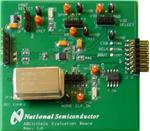
2. Board Assembly
The ADC161S626 evaluation board comes fully assembled and ready for use. Refer to the Bill of
Materials on page 14 for a description of components, to Figure 1 for major component placement,
and to the schematic on page 13.
2008 National Semiconductor Corporation
Rev: 1.0
Page 3 of 15
�JP11: VA
Select
JP8: VREF
Select
JP13: VIO
Select
J8: Analog
Input
J6:
WaveVision4.1
Connection
Y2: CLK
Oscillator
JP12: CLK
Select
TP15:
External CLK
Input
Figure 1 – Components Locations
3. Quick Start
The ADC161S626 evaluation board may be used in the ‘Stand-Alone mode’ to capture data with a
logic analyzer or other suitable test equipment, or it may be used in the ‘Computer mode’ with the
WV board. In both cases, the data may be analyzed with the WaveVision software.
3.1 Stand Alone Mode
Refer to Figure 1 for locations of test points and major components.
1. Connect a desired differential input signal across pins 3 and 5 of J8.
2008 National Semiconductor Corporation
Rev: 1.0
Page 4 of 15
�a. To create an ac-coupled input signal, stuff C21 and C22 with 1 uF capacitors but leave R30
and R34 unpopulated. To shift the input signal above ground, stuff R27, R28, R29, and R33
with 4.99k Ω resistors. Figure 2 shows the schematic for driving for ADC input with an
ac-coupled signal.
A-VBIAS
VA
A-VIN
J8
R30
NS
R27
R28
4.99k
4.99k
U7
ADC141S626
5P0V_EXT
1
2
3
4
5
VREF
R31
NS
C21 1u
1
2
3
+IN
C22 1u
-IN
R34
4
R29
R33
NS
HEADER 5/SM
4.99k
C38
NS
4.99k
C37
C31 470pF
5
VREF
VA
+IN
VIO
-IN
SCLK
GND
DOUT
GND
CSB
10
VA
9
VIO
8
SCLK
7
DOUT
6
CSB
NS
Figure 2 – Schematic to Drive ADC with an AC-Coupled Input Signal
b. To create a dc-coupled input signal, stuff R30 and R34 with 20 Ω resistors but leave C21,
C22, R27, R28, R29, and R33 unpopulated. Figure 3 shows the schematic for driving the
ADC input with a dc-coupled signal.
A-VBIAS
VA
A-VIN
J8
R30 20
R27
NS
R28
NS
U7
ADC141S626
5P0V_EXT
1
2
3
4
5
VREF
R31
NS
C21
NS
1
2
3
+IN
C22
-IN
NS
R34 20
4
R33
NS
R29
NS
C38
NS
C37
C31 470pF
5
VREF
+IN
VA
VIO
-IN
SCLK
GND
GND
DOUT
CSB
10
VA
9
VIO
8
SCLK
7
DOUT
6
CSB
NS
HEADER 5/SM
Figure 3 – Schematic to Drive ADC with a DC-Coupled Input Signal
2. Short pins 2 and 3 of JP11 to bias VA (analog voltage) via an external source. In this case,
connect a clean +2.7 V to +5.5 V power supply to TP12 and AGND.
3. There are three ways to bias the reference voltage VREF. Choose one of the following:
a. Short pins 1 and 2 of JP8 to use VA to bias VREF.
b. Short pins 2 and 3 of JP8 to use the 4.1V Reference Voltage (LM4132-4.1) to bias VREF.
c.
Supply a voltage less than or equal to VA at TP11 to source VREF externally. In this case,
remove the jumper from JP8.
2008 National Semiconductor Corporation
Rev: 1.0
Page 5 of 15
�4. There are two ways to bias the input/output driver voltage VIO. Choose one of the following:
a. Short pins 1 and 2 of JP13 to use an external source to bias VIO. In this case, connect a
clean +2.7 V to +5.5 V power supply to TP18 and AGND.
b. Short pins 2 and 3 of JP13 to use VA to bias VIO.
5. Remove the jumper from JP12 and the oscillator Y2 from its socket. The presence of Y2 could
add noise to the sampling process.
6. Apply signals to control the SPI interface.
a. Use a Logic Analyzer or other suitable test equipment to drive CSB (via 5 or pin 1 of J6)
and SCLK (via 6 or pin 2 of J6). Refer to the ADC161S626 datasheet to correctly drive
these pins.
b. Monitor DOUT at via 7 or pin 5 of J6 using a Logic Analyzer or a similar test equipment.
Note: Vias 5, 6, and 7 are 100 mil spaced apart.
3.2 Computer Mode
Refer to Figure 1 for locations of test points and major components.
1. Source the WV board with a clean +5 V supply and connect the ADC161S626 Evaluation
Board to the WV board via J6. Visit http://www.national.com/appinfo/adc/wv4.html for more
information on the WV board and its configuration.
2. Run the WaveVision software program (http://www.national.com/appinfo/adc/wv4.html). Version
4.4 or higher is required to interface the WV board with the ADC161S626 Evaluation Board.
While the program is loading, continue below.
3. Connect a desired differential input signal across pins 3 and 5 of J8.
a. To create an ac-coupled input signal, stuff C21 and C22 with 1 uF capacitors but leave R30
and R34 unpopulated. To shift the input signal above ground, stuff R27, R28, R29, and R33
with 4.99k Ω resistors. The schematic for this mode can be seen in figure 2.
b. To create a dc-coupled input signal, stuff R30 and R34 with 20 Ω resistors but leave C21,
C22, R27, R28, R29, and R33 unpopulated. Refer to figure 3 for the schematic.
4. There are two ways to bias the analog voltage VA. Choose one of the following:
a. Short pins 1 and 2 of JP11 to bias VA via the +5.0V from the WV board.
b. Short pins 2 and 3 of JP11 to bias VA (analog voltage) via an external source. In this case,
connect a clean +2.7 V to +5.5 V power supply to TP12 and AGND.
5. There are three ways to bias the reference voltage VREF. Choose one of the following:
c.
Short pins 1 and 2 of JP8 to use VA to bias VREF.
d. Short pins 2 and 3 of JP8 to use the 4.1V Reference Voltage (LM4132-4.1) to bias VREF.
2008 National Semiconductor Corporation
Rev: 1.0
Page 6 of 15
�e. Supply a voltage less than or equal to VA at TP11 to source VREF externally. In this case,
remove the jumper from JP8.
6. There are two ways to bias the input/output driver voltage VIO. Choose one of the following:
a. Short pins 1 and 2 of JP13 to use an external source to bias VIO. In this case, connect a
clean +2.7 V to +5.5 V power supply to TP18 and AGND.
b. Short pins 2 and 3 of JP13 to use VA to bias VIO.
7. There are two ways to select a clock source. Choose one of the following:
a. Short pins 1 and 2 of JP12 to use an external crystal oscillator. Then, install an appropriate
crystal oscillator into socket Y2.
b. Short pins 2 and 3 of JP12 to use a signal generator as an oscillator. Connect a clean
signal generator with 3.3 V CMOS logic levels to TP15 and AGND. Remember not to place
any crystal oscillator into socket Y2.
8. After configuring the ADC161S626 Evaluation board and connecting the board to the WV
board, refer to section 5 - Software Operation and Settings to use the WaveVision software
program to analyze the ADC161S626.
4. Functional Description
Table I describes the functions of the jumpers on the ADC161S626 Evaluation Board. The board
schematic is shown on page 11.
Jumper
Name
JP8
VREF
JP11
VA
JP12
CLK
JP13
VIO
Pins 1 & 2
Select VA to source VREF
Pins 2 & 3
Select +4.1V Voltage Regular
(U4) to source VREF
Select +5.0V from the WV board to
Select an external power supply
source VA.
to source VA.
Select on-board clock OSC Y2.
Select clock OSC at TP15.
Select an external power supply to
source VIO.
Select VA to source VIO.
Table I – Jumper Functions
2008 National Semiconductor Corporation
Rev: 1.0
Page 7 of 15
�4.1 Analog Input Signal
The ADC161S626 has dual differential inputs as shown in figure 4. The signal to be digitized should
be applied across pins 3 and 5 of J8.
VREF
2
VCM
V
VCM - REF
2
VCM +
RS
+
SRC
CS
ADC141S626
-
RS
VREF
2
VCM
V
VCM - REF
2
VCM +
Figure 4 – Differential Input
Generating an ac-coupled input signal only requires stuffing capacitors C21 and C22 with 1uF
capacitors. For signal generators that do not have an offset function, stuff resistors R27, R28, R29,
and R33 with 4.99k Ω resistors to shift the ac-coupled input signal above ground. Leave resistors
R30, R34, and capacitors C37 and C38 unpopulated. Refer to figure 2 to see the schematic for
driving the ADC input with an ac-coupled signal.
To properly create a dc-coupled input signal, stuff R30 and R34 with 20 Ω resistors. However,
leave capacitors C21, C22, and resistors R27, R28, R29, and R33 unpopulated. A schematic of
this explanation can be seen in figure 3.
For single-ended operation, the non-inverting input of the ADC can be driven with a sinusoidal input
signal, and the inverting input of the ADC can be driven with a dc voltage. The sinusoidal input
signal driving the non-inverting input should have a minimum to maximum value range that is equal
to or less than twice the reference voltage. The inverting input should be biased at a common
mode voltage, VCM, which is a stable voltage that is halfway between these maximum and
minimum values. Figure 5 shows the ADC161S626 being driven by a single-ended source.
2008 National Semiconductor Corporation
Rev: 1.0
Page 8 of 15
�VCM + VREF
VCM
VCM - VREF
RS
+
CS
SRC
ADC141S626
-
VCM
Figure 5 – Single-Ended Input
Dynamic input signals should be applied through a lowpass or bandpass filter to eliminate the noise
and harmonics commonly associated with signal sources. To accurately evaluate the performance
of the ADC161S626, the source must be better than -100dBFS THD (Total Harmonic Distortion).
4.2 ADC Reference Circuitry
This evaluation board includes three options to source the voltage reference, VREF. These options
include selecting a fixed +4.1V voltage reference to source VREF, using VA to source VREF, or
using a power supply to source VREF. To select the +4.1V reference, short pins 2 & 3 of JP8. To
select VA, short pins 1 & 2 of JP8. If it is desirable to provide an external reference voltage, the
jumper must be removed from JP8, and TP11 may be driven directly by a power supply set
between +2.7 V and +5.5 V.
4.3 SPI Interface
The ADC161S626 requires three SPI input and output pins. These pins are Serial Clock (SCLK),
Chip Select Bar (CSB), and Digital Data Output (DOUT). The user must provide input signals for
SCLK and CSB in order to receive an output signal DOUT from the ADC161S626. Further
descriptions of those pins are discussed below.
4.3.1
Serial Clock (SCLK)
The crystal-based oscillator provided on the evaluation board is selected by shorting pins 1 & 2 of
JP12. It is best to remove any external signal generator from TP15 when using this oscillator to
reduce any unnecessary noise.
2008 National Semiconductor Corporation
Rev: 1.0
Page 9 of 15
�This board will also accept a clock signal from an external source by connecting that source to
TP15 and AGND and shorting pins 2 & 3 of JP12. The input applied at TP15 is 51 ohm terminated
by R45. The external clock signal must meet the 3.3 V CMOS input requirements. If the external
source is an ac-source centered around ground, populate R42 and R43 with 4.99k Ω resistors to
shift the clock level. To reduce any unnecessary noise, it is best to remove the oscillator at Y2 when
using an external clock source.
Regardless of the clock source selected by JP12, the clock signal is designed to be routed off the
ADC161S626 Evaluation Board to the WV board. This assumes a ‘Computer mode’ operation of
the evaluation board. For applications utilizing the evaluation board in ‘Stand-Alone mode’, the
clock is applied directly at via 6 or at pin 3 of J6.
4.3.2
Chip Select Bar (CSB)
In the ‘Stand-Alone mode’, CSB has to be driven directly at via 5 or at pin 1 of J6. In the ‘Computer
mode’, CSB can be monitored at via 5 or at pin 1 of J6. The signal level for CSB needs to be TTL
compatible. See the ADC161S626 datasheet for logic threshold limits.
4.3.3
Digital Data Output (DOUT)
In the ‘Stand-Alone mode’, DOUT can be monitored at via 7 or at pin 5 of J6. In the ‘Computer
mode’, DOUT is monitored by the WV board.
The signal level for DOUT is CMOS and TTL
compatible. See the ADC161S626 datasheet for logic output levels.
4.4 Power Supply Connection
Voltages VA and VIO can be driven using an external power supply.
In the ‘Stand-Alone mode’, the user has to use the external power supply to drive VA. Do not short
pins 1 and 2 of JP11 when operating in the ‘Stand-Alone mode’. To drive VA correctly, short pins 2
and 3 of JP11, and drive TP12 with an external power supply set between +2.7 V and +5.5 V.
In the ‘Computer mode’, VA can be driven with an external power supply or with the +5.0V from WV
board. Short pins 1 and 2 of JP11 to automatically use the +5.0 V from the WV board.
The driver input/output voltage VIO can also be driven from VA or externally with a power supply.
To use the voltage VA to drive VIO, short pins 2 and 3 of JP13. To drive VIO with an external
source, short pins 1 and 2 of JP13, then set TP18 to a voltage between +2.7 V and +5.5V.
2008 National Semiconductor Corporation
Rev: 1.0
Page 10 of 15
�5. Software Operation and Settings
The WaveVision software is included with the WV board and the latest version can be downloaded
for free from National's web site at http://www.national.com/appinfo/adc/wv4.html. To install this
software, follow the procedure in the WV board User's Guide. Once the software is installed, run
and set it up as follow:
1. After configuring the ADC161S626 Evaluation Board and connecting it to the WV board as
discussed in Section 3.2, connect the WV board to the host computer with a USB cable.
2. From the WaveVision software main menu, go to ‘Settings’, then ‘Capture Settings’ and
select the following from the menu:
a. Board Type: WaveVision 4.0 (USB)
b. Number of Samples: 2k to 32k, as desired
c.
Data Format: Two’s Complement
3. Click on the "Reset" button and await the firmware to download.
4. Click on the "Close" button.
5. Click on “Acquire” then “Samples” from the Main Menu (you can also press the F1 shortcut
key). If a dialog box opens, select “Discard” or press the Escape key to start collecting new,
updated samples.
A plot of the selected number of samples will be displayed. Make sure there is no clipping of data
samples. If clipping occurs, lower the analog input voltage. The samples may be further analyzed
by clicking on the magnifying glass icon, then clicking and dragging across a specific area of the
plot for better data inspection.
To view an FFT of the data captured, click on the ‘FFT’ tab. This plot may be zoomed in like the
data plot. A display of dynamic performance parameters in the form of SINAD, SNR, THD, SFDR
and ENOB will be displayed at the top right hand corner of the FFT plot.
Acquired data may be saved to a file. Plots may also be exported as graphics.
For more information, view the WV board’s User Guide at
http://www.national.com/appinfo/adc/wv4.html.
2008 National Semiconductor Corporation
Rev: 1.0
Page 11 of 15
�6. Evaluation Board Specifications
Board Size:
2.250" x 2.3" (7.6 cm x 7.6 cm)
Power
Min: +2.7 V, Max: +5.5 V,
Requirements
100mA
Clock Frequency
800 kHz to 4.0 MHz
100 mA
Range:
Analog Input
0 V to (2 * VREF) Vpp
Table II – ADC161S626 Evaluation Board Specifications
7. Tables of Test Points, Jumpers, and Connectors
Test Points on the ADC161S626 Evaluation Board
TP11: VREF
VREF test point. Located at the top left area of the board.
TP12: 5P0V_EXT
VA external supply. Located at the middle top area of the board.
TP13: AGND
Ground. Located at the middle top area of the board.
TP14: 3P3V
+3.3V test point. Located at the middle right area of the board.
TP15: CLK_IN
External Clock. Located at the bottom middle of the board.
TP16: AGND
Ground. Located at the bottom middle of the board.
TP17: AGND
Ground. Located at the top left area of the board.
TP18: VIO_EXT
VIO external supply. Located at the top right corner of the board.
TP19: AGND
Ground. Located at the top right corner of the board.
TP21: AGND
Ground. Located at the top right corner of the board.
TP22: VA
VA test point. Located at the middle top area of the board.
TP23: AGND
Ground. Located at the middle top area of the board.
Connectors on the ADC161S626 Evaluation Board
J6: WV4S
14 pin dual row right angle male header. Connect to WV board.
J8: VIN
Five pin male header. Differential AC and DC input.
Selection Jumpers on the ADC161S626 Evaluation Board (Refer to Table 1 in Section 4.0 for configuration details)
JP8: VREF SELECT
Selects reference source for VREF. Located at the top left corner of the board.
JP11: VA SELECT
Selects source for VA. Located at the top middle area of the board.
JP12: CLK SELECT
Selects source for the clock. Located at the bottom middle area of the board.
JP13: VIO SELECT
Selects source for VIO. Located on the top right corner of the board.
JP14: OSC Enable
Not Stuffed. If jumpered, pin 1 of the oscillator is grounded. Located on the bottom left
corner of the board to the left of Y2.
2008 National Semiconductor Corporation
Rev: 1.0
Page 12 of 15
�8. Hardware Schematic
VA
VREF SELECTION
2
3
VREF
EN
TP21
AGND
D5
RED LED
4
VA SELECTION
VREF
TP11
JP11
VA SELECTION
External Supply
TP17
AGND 1
C19
TP12
5P0V_EXT 1
C20
+
10uF
5.0 V from WV
5P0V_EXT
5P0V_WV
3
2
1
1
C25
10uF
TP13 1
AGND
0.1uF
TP23
AGND 1
A-VIN
C21
1
2
3
4
5
+IN
-IN
R29 NS
C37
NS
1
NS
2
3
R34
NS
20
4
R33
NS
C38
NS
C31 470pF
5
U7
ADC141S626
VREF
+IN
VA
VIO
-IN
SCLK
GND
DOUT
GND
CSB
10
SCLK DOUT TP19
VIA6 VIA7 AGND
1
R28
NS
R31
NS
C22
CSB
VIA5
1
R27
NS
R30 20
C32
0.1uF
+
1
C28
10uF
1
VA
5P0V_EXT
C26
0.1uF
+
VA
TP22
1
A-VBIAS
J8
TP18
VIO_EXT
1
VA
VA
VIN
Vref
VA
5
GND
JP13
VIO SELECTION
+
C18
10uF
NC
VA
1
1
R48
510
3
2
1
U4
LM4132-4.1
VIO SELECTION
VA
3
2
1
Voltage Reference
JP8
VREF SELECT
J6
WV4S
VA
WV4S
9
CSB
CSB_WV
1
2
8
SCLK
SCLK_WV
3
4
DOUT
DOUT_WV
5
6
7
8
9
10
7
R46
510
6
CLKSEND_WV
HEADER 5/SM
SDA_WV
11
12 SCL_WV
13
14
5P0V_WV
CLK SELECTION
3P3V_WV
R41
51
External Oscillator
2
5P0V_WV
JP12
CLK SELECT
3P3V
TP14
3P3V
1
1
3
3P3V_WV
C27
0.1uF
3P3V_WV
TP15
CLK_IN
Rev: 1.0
Page 13 of 15
5
6
SCL
SDA
GND
A2
3
4
8
7
WP
3P3V_WV
TP16
AGND 1
2008 National Semiconductor Corporation
A1
A0
OSC ENABLE
D4
RED LED
1
C29
0.1uF
VCC
R47
200
JP14
2
OE
Y2
OSC (THROUGH-HOLE)
1
1
R45 51
OUT
GND
8
R44
0
7
R42
NS
VDD
14
R43 NS
U6
24C02
�9. ADC161S626 Evaluation Board Bill of Materials
Item
Qunty
Reference
Part
Source
Source Part #
1
4
2
5
C18,C19,C25,C28
10uF
N/A
N/A
C20,C26,C27,C29,C32
0.1uF
N/A
3
2
C21,C22
N/A
Not Stuffed (1uF)
N/A
N/A
4
1
C31
5
2
C37,C38
N/A
6
2
D4,D5
7
1
JP8
3-Pin Post Header
Digikey
S1011E-36-ND
8
1
JP11
3-Pin Post Header
Digikey
S1011E-36-ND
470pF
N/A
Not Stuffed (0.1uF)
N/A
N/A
RED LED
Digikey
516-1440-1-ND
9
1
JP12
3-Pin Post Header
Digikey
S1011E-36-ND
10
1
JP13
3-Pin Post Header
Digikey
S1011E-36-ND
11
1
JP14
Not Stuffed (Jumper)
N/A
N/A
J6
RIGHT ANGLE MALE
HEADER 100Mil
Digikey
S5803-21-ND
12
1
13
1
J8
14
6
R27,R28,R29,R33,R42,R43
HEADER 5/SM
N/A
N/A
Not Stuffed (4.99k ohm)
N/A
15
2
R30,R34
N/A
20
N/A
N/A
16
1
R31
Not Stuffed
N/A
N/A
17
2
R41, R45
51
N/A
N/A
18
1
R44
0
N/A
N/A
20
1
R47
200
N/A
N/A
21
1
R48
510
N/A
N/A
22
1
R46
510
N/A
N/A
23
1
TP11
Test Pin for VREF
Digikey
5003K-ND
24
1
TP12
Test Pin for 5P0V_EXT
Digikey
5003K-ND
25
6
TP13,TP16,TP17,TP19,TP21,TP23
Test Pin for AGND
Digikey
5011K-ND
26
1
TP14
Test Pin for 3P3V
Digikey
5003K-ND
27
1
TP15
Test pin for CLK_IN
Digikey
5003K-ND
28
1
TP18
Test Pin for VIO_EXT
Digikey
5003K-ND
29
1
TP22
Test pin for VA
Digikey
5003K-ND
30
1
U4
LM4132-4.1
N/A
N/A
31
1
U6
24C02
N/A
N/A
32
1
U7
ADC161S626
N/A
N/A
33
1
VIA5
CSB
Digikey
N/A
34
1
VIA6
SCLK
Digikey
N/A
35
1
VIA7
36
1
Y2
2008 National Semiconductor Corporation
DOUT
Digikey
N/A
OSC (THROUGH-HOLE)
Digikey
A400-ND
Rev: 1.0
Page 14 of 15
�BY USING THIS PRODUCT, YOU ARE AGREEING TO BE BOUND BY THE TERMS AND CONDITIONS OF NATIONAL
SEMICONDUCTOR'S END USER LICENSE AGREEMENT. DO NOT USE THIS PRODUCT UNTIL YOU HAVE READ AND
AGREED TO THE TERMS AND CONDITIONS OF THAT AGREEMENT. IF YOU DO NOT AGREE WITH THEM, CONTACT
THE VENDOR WITHIN TEN (10) DAYS OF RECEIPT FOR INSTRUCTIONS ON RETURN OF THE UNUSED PRODUCT FOR
A REFUND OF THE PURCHASE PRICE PAID, IF ANY.
The ADC161S626 Evaluation Board is intended for product evaluation purposes only and is not intended for resale to end
consumers, is not authorized for such use and is not designed for compliance with European EMC Directive 89/336/EEC, or for
compliance with any other electromagnetic compatibility requirements.
National Semiconductor Corporation does not assume any responsibility for use of any circuitry or software supplied or described.
No circuit patent licenses are implied.
LIFE SUPPORT POLICY
NATIONAL'S PRODUCTS ARE NOT AUTHORIZED FOR USE AS CRITICAL COMPONENTS IN LIFE SUPPORT DEVICES OR
SYSTEMS WITHOUT THE EXPRESS WRITTEN APPROVAL OF THE PRESIDENT OF NATIONAL SEMICONDUCTOR
CORPORATION. As used herein:
1. Life support devices or systems are devices or systems which, (a) are intended for surgical implant into the body, or (b)
support or sustain life, and whose failure to perform, when properly used in accordance with instructions for use provided in
the labeling, can be reasonably expected to result in a significant injury to the user.
2. A critical component is any component in a life support device or system whose failure to perform can be reasonably
expected to cause the failure of the life support device or system, or to affect its safety or effectiveness.
National Semiconductor Corporation
Americas
Tel:
1-800-272-9959
Fax: 1-800-737-7018
Email: support@nsc.com
National Semiconductor Europe
Fax: +49 (0) 1 80-530 85 86
Email: europe.support@nsc.com
Deutsch Tel: +49 (0) 699508 6208
English Tel: +49 (0) 870 24 0 2171
French Tel: +49 (0) 141 91 8790
National Semiconductor
Asia Pacific Customer
Response Group
Tel: 65-2544466
Fax: 65-2504466
Email:sea.support@nsc.com
National
Semiconductor
Japan Ltd.
Tel: 81-3-5639-7560
Fax: 81-3-5639-7507
www.national.com
National does not assume any responsibility for any circuitry described, no circuit patent licenses are implied and National reserves the right at any
time without notice to change said circuitry and specification.
2008 National Semiconductor Corporation
Rev: 1.0
Page 15 of 15
�IMPORTANT NOTICE
Texas Instruments Incorporated and its subsidiaries (TI) reserve the right to make corrections, modifications, enhancements, improvements,
and other changes to its products and services at any time and to discontinue any product or service without notice. Customers should
obtain the latest relevant information before placing orders and should verify that such information is current and complete. All products are
sold subject to TI’s terms and conditions of sale supplied at the time of order acknowledgment.
TI warrants performance of its hardware products to the specifications applicable at the time of sale in accordance with TI’s standard
warranty. Testing and other quality control techniques are used to the extent TI deems necessary to support this warranty. Except where
mandated by government requirements, testing of all parameters of each product is not necessarily performed.
TI assumes no liability for applications assistance or customer product design. Customers are responsible for their products and
applications using TI components. To minimize the risks associated with customer products and applications, customers should provide
adequate design and operating safeguards.
TI does not warrant or represent that any license, either express or implied, is granted under any TI patent right, copyright, mask work right,
or other TI intellectual property right relating to any combination, machine, or process in which TI products or services are used. Information
published by TI regarding third-party products or services does not constitute a license from TI to use such products or services or a
warranty or endorsement thereof. Use of such information may require a license from a third party under the patents or other intellectual
property of the third party, or a license from TI under the patents or other intellectual property of TI.
Reproduction of TI information in TI data books or data sheets is permissible only if reproduction is without alteration and is accompanied
by all associated warranties, conditions, limitations, and notices. Reproduction of this information with alteration is an unfair and deceptive
business practice. TI is not responsible or liable for such altered documentation. Information of third parties may be subject to additional
restrictions.
Resale of TI products or services with statements different from or beyond the parameters stated by TI for that product or service voids all
express and any implied warranties for the associated TI product or service and is an unfair and deceptive business practice. TI is not
responsible or liable for any such statements.
TI products are not authorized for use in safety-critical applications (such as life support) where a failure of the TI product would reasonably
be expected to cause severe personal injury or death, unless officers of the parties have executed an agreement specifically governing
such use. Buyers represent that they have all necessary expertise in the safety and regulatory ramifications of their applications, and
acknowledge and agree that they are solely responsible for all legal, regulatory and safety-related requirements concerning their products
and any use of TI products in such safety-critical applications, notwithstanding any applications-related information or support that may be
provided by TI. Further, Buyers must fully indemnify TI and its representatives against any damages arising out of the use of TI products in
such safety-critical applications.
TI products are neither designed nor intended for use in military/aerospace applications or environments unless the TI products are
specifically designated by TI as military-grade or "enhanced plastic." Only products designated by TI as military-grade meet military
specifications. Buyers acknowledge and agree that any such use of TI products which TI has not designated as military-grade is solely at
the Buyer's risk, and that they are solely responsible for compliance with all legal and regulatory requirements in connection with such use.
TI products are neither designed nor intended for use in automotive applications or environments unless the specific TI products are
designated by TI as compliant with ISO/TS 16949 requirements. Buyers acknowledge and agree that, if they use any non-designated
products in automotive applications, TI will not be responsible for any failure to meet such requirements.
Following are URLs where you can obtain information on other Texas Instruments products and application solutions:
Products
Applications
Audio
www.ti.com/audio
Automotive and Transportation www.ti.com/automotive
Amplifiers
amplifier.ti.com
Communications and Telecom www.ti.com/communications
Data Converters
dataconverter.ti.com
Computers and Peripherals
www.ti.com/computers
DLP® Products
www.dlp.com
Consumer Electronics
www.ti.com/consumer-apps
DSP
dsp.ti.com
Energy and Lighting
www.ti.com/energy
Clocks and Timers
www.ti.com/clocks
Industrial
www.ti.com/industrial
Interface
interface.ti.com
Medical
www.ti.com/medical
Logic
logic.ti.com
Security
www.ti.com/security
Power Mgmt
power.ti.com
Space, Avionics and Defense
www.ti.com/space-avionics-defense
Microcontrollers
microcontroller.ti.com
Video and Imaging
www.ti.com/video
RFID
www.ti-rfid.com
OMAP Mobile Processors
www.ti.com/omap
Wireless Connectivity
www.ti.com/wirelessconnectivity
TI E2E Community Home Page
e2e.ti.com
Mailing Address: Texas Instruments, Post Office Box 655303, Dallas, Texas 75265
Copyright © 2012, Texas Instruments Incorporated
�