Product
Folder
Sample &
Buy
Support &
Community
Tools &
Software
Technical
Documents
ADC32J22, ADC32J23, ADC32J24, ADC32J25
SBAS668A – MAY 2014 – REVISED JUNE 2015
ADC32J2x Dual-Channel, 12-Bit, 50-MSPS to 160-MSPS, Analog-to-Digital Converter
with JESD204B Interface
1 Features
3 Description
•
•
•
•
•
The ADC32J2x is a high-linearity, ultra-low power,
dual-channel, 12-bit, 50-MSPS to 160-MSPS, analogto-digital converter (ADC) family. The devices are
designed specifically to support demanding, high
input frequency signals with large dynamic range
requirements. A clock input divider allows more
flexibility for system clock architecture design and the
SYSREF
input
enables
complete
system
synchronization. The devices support JESD204B
interfaces in order to reduce the number of interface
lines, thus allowing for high system integration
density. The JESD204B interface is a serial interface,
where the data of each ADC are serialized and output
over only one differential pair. An internal phaselocked loop (PLL) multiplies the incoming ADC
sampling clock by 20 to derive the bit clock that is
used to serialize the 12-bit data from each channel.
The devices support subclass 1 with interface speeds
up to 3.2 Gbps.
1
•
•
•
•
•
•
•
Dual Channel
12-Bit Resolution
Single 1.8-V Supply
Flexible Input Clock Buffer with Divide-by-1, -2, -4
SNR = 70.3 dBFS, SFDR = 88 dBc at
fIN = 70 MHz
Ultralow Power Consumption:
– 227 mW/Ch at 160 MSPS
Channel Isolation: 105 dB
Internal Dither
JESD204B Serial Interface:
– Subclass 0, 1, 2 Compliant up to 3.2 Gbps
– Supports One Lane per ADC up to 160 MSPS
Support for Multichip Synchronization
Pin-to-Pin Compatible with 14-Bit Version
(ADC32J4X)
Package: VQFN-48 (7 mm × 7 mm)
Device Information(1)
PART NUMBER
PACKAGE
2 Applications
•
•
•
•
•
•
•
•
•
•
(1) For all available packages, see the package option addendum
at the end of the datasheet.
7.00 mm × 7.00 mm
FFT with Dither On
(fS = 160 MSPS, SNR = 70.3 dBFS, fIN = 10 MHz,
SFDR = 92.6 dBc)
0
-10
-20
-30
Amplitude (dBFS)
Multi-Carrier, Multi-Mode Cellular Base Stations
Radar and Smart Antenna Arrays
Munitions Guidance
Motor Control Feedback
Network and Vector Analyzers
Communications Test Equipment
Nondestructive Testing
Microwave Receivers
Software Defined Radios (SDRs)
Quadrature and Diversity Radio Receivers
VQFN (48)
BODY SIZE (NOM)
ADC32J2X
-40
-50
-60
-70
-80
-90
-100
-110
-120
0
16
32
48
Frequency (MHz)
64
80
D201
1
An IMPORTANT NOTICE at the end of this data sheet addresses availability, warranty, changes, use in safety-critical applications,
intellectual property matters and other important disclaimers. PRODUCTION DATA.
�ADC32J22, ADC32J23, ADC32J24, ADC32J25
SBAS668A – MAY 2014 – REVISED JUNE 2015
www.ti.com
Table of Contents
1
2
3
4
5
6
7
Features ..................................................................
Applications ...........................................................
Description .............................................................
Revision History.....................................................
Device Comparison Table.....................................
Pin Configuration and Functions .........................
Specifications.........................................................
7.1
7.2
7.3
7.4
7.5
7.6
7.7
7.8
7.9
7.10
7.11
7.12
7.13
7.14
7.15
7.16
7.17
7.18
1
1
1
2
3
3
5
Absolute Maximum Ratings ...................................... 5
ESD Ratings.............................................................. 5
Recommended Operating Conditions....................... 5
Thermal Information .................................................. 6
Electrical Characteristics........................................... 6
Electrical Characteristics: ADC32J22, ADC32J23.... 7
Electrical Characteristics: ADC32J24, ADC32J25.... 7
AC Performance: ADC32J25 .................................... 8
AC Performance: ADC32J24 .................................. 10
AC Performance: ADC32J23 ................................ 12
AC Performance: ADC32J22 ................................ 14
Digital Characteristics ........................................... 16
Timing Requirements ............................................ 17
Typical Characteristics: ADC32J25 ...................... 18
Typical Characteristics: ADC32J24 ...................... 24
Typical Characteristics: ADC32J23 ...................... 30
Typical Characteristics: ADC32J22 ...................... 36
Typical Characteristics: Common Plots ................ 42
7.19 Typical Characteristics: Contour Plots .................. 43
8
Parameter Measurement Information ................ 44
9
Detailed Description ............................................ 46
8.1 Timing Diagrams ..................................................... 44
9.1
9.2
9.3
9.4
9.5
9.6
Overview .................................................................
Functional Block Diagram .......................................
Feature Description.................................................
Device Functional Modes........................................
Programming...........................................................
Register Maps .........................................................
46
46
46
53
54
58
10 Applications and Implementation...................... 72
10.1 Application Information.......................................... 72
10.2 Typical Applications .............................................. 73
11 Power Supply Recommendations ..................... 75
12 Layout................................................................... 76
12.1 Layout Guidelines ................................................. 76
12.2 Layout Example .................................................... 76
13 Device and Documentation Support ................. 77
13.1
13.2
13.3
13.4
13.5
Related Links ........................................................
Community Resources..........................................
Trademarks ...........................................................
Electrostatic Discharge Caution ............................
Glossary ................................................................
77
77
77
77
77
14 Mechanical, Packaging, and Orderable
Information ........................................................... 77
4 Revision History
Changes from Original (May 2015) to Revision A
•
2
Page
Changed from product preview to production data ................................................................................................................ 1
Submit Documentation Feedback
Copyright © 2014–2015, Texas Instruments Incorporated
Product Folder Links: ADC32J22 ADC32J23 ADC32J24 ADC32J25
�ADC32J22, ADC32J23, ADC32J24, ADC32J25
www.ti.com
SBAS668A – MAY 2014 – REVISED JUNE 2015
5 Device Comparison Table
INTERFACE
Serial LVDS
JESD204B
RESOLUTION
(Bits)
25 MSPS
50 MSPS
80 MSPS
125 MSPS
160 MSPS
12
ADC3221
ADC3222
ADC3223
ADC3224
—
14
ADC3241
ADC3242
ADC3243
ADC3244
—
12
—
ADC32J22
ADC32J23
ADC32J24
ADC32J25
14
—
ADC32J42
ADC32J43
ADC32J44
ADC32J45
6 Pin Configuration and Functions
DAM
DAP
AVDD
DBM
DBP
SYNCP~
SYNCM~
NC
NC
AVDD
NC
NC
RGZ Package
48-Pin VQFN
Top View
48
47
46
45
44
43
42
41
40
39
38
37
OVRA
1
36
OVRB
NC
2
35
NC
DVDD
3
34
DVDD
AVDD
4
33
PDN
AVDD
5
32
AVDD
NC
6
31
NC
NC
7
30
NC
AVDD
8
29
AVDD
AVDD
9
28
AVDD
INAP
10
27
INBP
INAM
11
26
INBM
AVDD
12
25
AVDD
13
14
15
16
17
18
19
20
21
22
23
24
SCLK
SDATA
SEN
SDOUT
AVDD
CLKM
CLKP
AVDD
RESET
SYSREFP
SYSREFM
VCM
GND Pad
(Back Side)
Copyright © 2014–2015, Texas Instruments Incorporated
Submit Documentation Feedback
Product Folder Links: ADC32J22 ADC32J23 ADC32J24 ADC32J25
3
�ADC32J22, ADC32J23, ADC32J24, ADC32J25
SBAS668A – MAY 2014 – REVISED JUNE 2015
www.ti.com
Pin Functions
PIN
NAME
I/O
NO.
DESCRIPTION
AVDD
4, 5, 8, 9, 12, 17,
20, 25, 28, 29, 32,
39, 46
I
Analog 1.8-V power supply
CLKM
18
I
Negative differential clock input for the ADC
CLKP
19
I
Positive differential clock input for the ADC
DAM
48
O
Negative serial JESD204B output for channel A
DAP
47
O
Positive serial JESD204B output for channel A
DBM
45
O
Negative serial JESD204B output for channel B
DBP
44
O
Positive serial JESD204B output for channel B
DVDD
3,34
I
Digital 1.8-V power supply
GND
PowerPAD™
I
Ground, 0 V
INAM
11
I
Negative differential analog input for channel A
INAP
10
I
Positive differential analog input for channel A
INBM
26
I
Negative differential analog input for channel B
INBP
27
I
Positive differential analog input for channel B
2, 6, 7, 30, 31, 35,
37, 38, 40, 41
—
Do not connect
OVRA
1
O
Overrange indicator for channel A
OVRB
36
O
Overrange indicator for channel B
PDN
33
I
Power-down control. This pin has an internal 150-kΩ pulldown resistor.
RESET
21
I
Hardware reset; active high. This pin has an internal 150-kΩ pulldown resistor.
SCLK
13
I
Serial interface clock input. This pin has an internal 150-kΩ pulldown resistor.
SDATA
14
I
Serial Interface data input. This pin has an internal 150-kΩ pulldown resistor.
SDOUT
16
O
Serial interface data output
SEN
15
I
Serial interface enable; active low.
This pin has an internal 150-kΩ pullup resistor to AVDD.
SYNCM~
42
I
Positive JESD204B synch input
SYNCP~
43
I
Negative JESD204B synch input
SYSREFM
23
I
Negative external SYSREF input
SYSREFP
22
I
Positive external SYSREF input
VCM
24
O
Common-mode voltage output for analog inputs
NC
4
Submit Documentation Feedback
Copyright © 2014–2015, Texas Instruments Incorporated
Product Folder Links: ADC32J22 ADC32J23 ADC32J24 ADC32J25
�ADC32J22, ADC32J23, ADC32J24, ADC32J25
www.ti.com
SBAS668A – MAY 2014 – REVISED JUNE 2015
7 Specifications
7.1 Absolute Maximum Ratings
over operating free-air temperature range (unless otherwise noted) (1)
Supply voltage range, AVDD
Supply voltage range, DVDD
Voltage applied to input pins:
Temperature range
MAX
UNIT
2.1
V
–0.3
2.1
V
INAP, INBP
–0.3
AVDD + 0.3
V
CLKP, CLKM
–0.3
AVDD + 0.3
V
SYSREFP, SYSREFM, SYNCP~, SYNCM~
–0.3
AVDD + 0.3
V
SCLK, SEN, SDATA, RESET, PDN
–0.3
AVDD + 0.3
V
Operating free-air, TA
–40
85
°C
125
°C
150
°C
Operating junction, TJ
Storage, Tstg
(1)
MIN
–0.3
–65
Stresses beyond those listed under Absolute Maximum Ratings may cause permanent damage to the device. These are stress ratings
only, which do not imply functional operation of the device at these or any other conditions beyond those indicated under Recommended
Operating Conditions. Exposure to absolute-maximum-rated conditions for extended periods may affect device reliability.
7.2 ESD Ratings
V(ESD)
(1)
Human body model (HBM), per ANSI/ESDA/JEDEC JS-001, all pins (1)
Electrostatic discharge
VALUE
UNIT
±2000
V
JEDEC document JEP155 states that 500-V HBM allows safe manufacturing with a standard ESD control process.
7.3 Recommended Operating Conditions
over operating free-air temperature range (unless otherwise noted)
MIN
NOM
MAX
UNIT
SUPPLIES
AVDD
Analog supply voltage range
1.7
1.8
1.9
V
DVDD
Digital supply voltage range
1.7
1.8
1.9
V
ANALOG INPUT
VID
Differential input voltage
VIC
Input common-mode voltage
For input frequencies < 450 MHz
2
VPP
For input frequencies < 600 MHz
1
VPP
VCM ± 0.025
V
CLOCK INPUT
Input clock frequency
Sampling clock frequency
Input clock amplitude (differential)
160 (1)
25
MSPS
Sine wave, ac-coupled
1.5
V
LPECL, ac-coupled
1.6
V
LVDS, ac-coupled
0.7
V
Input clock duty cycle
50%
Input clock common-mode voltage
0.95
V
DIGITAL OUTPUTS
CLOAD
Maximum external load capacitance
from each output pin to GND
3.3
pF
RLOAD
Single-ended load resistance
100
Ω
(1)
With the clock divider enabled by default for divide-by-1. Maximum sampling clock frequency for the divide-by-4 option is 640 MSPS.
Copyright © 2014–2015, Texas Instruments Incorporated
Submit Documentation Feedback
Product Folder Links: ADC32J22 ADC32J23 ADC32J24 ADC32J25
5
�ADC32J22, ADC32J23, ADC32J24, ADC32J25
SBAS668A – MAY 2014 – REVISED JUNE 2015
www.ti.com
7.4 Thermal Information
ADC32J2x
THERMAL METRIC (1)
RGZ (VQFN)
UNIT
48 PINS
RθJA
Junction-to-ambient thermal resistance
25.7
°C/W
RθJC(top)
Junction-to-case (top) thermal resistance
18.9
°C/W
RθJB
Junction-to-board thermal resistance
3.0
°C/W
ψJT
Junction-to-top characterization parameter
0.2
°C/W
ψJB
Junction-to-board characterization parameter
3
°C/W
RθJC(bot)
Junction-to-case (bottom) thermal resistance
0.5
°C/W
(1)
For more information about traditional and new thermal metrics, see the Semiconductor and IC Package Thermal Metrics application
report, SPRA953.
7.5 Electrical Characteristics
Typical values are at TA = 25°C, full temperature range is TMIN = –40°C to TMAX = 85°C, Maximum sampling rate, 50% clock
duty cycle, AVDD = DVDD = 1.8 V, and –1-dBFS differential input, unless otherwise noted.
PARAMETER
TEST CONDITIONS
MIN
TYP
MAX
UNIT
ANALOG INPUT
Differential input full-scale
2.0
VPP
Input resistance
Differential at dc
6.5
kΩ
Input capacitance
Differential at dc
5.2
pF
0.95
V
VCM common-mode voltage output
VCM output current capability
10
mA
Input common-mode current
Per analog input pin
1.5
µA/MSPS
Analog input bandwidth (3 dB)
50-Ω differential source driving 50-Ω
termination across INP and INM
450
MHz
DC ACCURACY
Offset error
EG(REF)
Gain error as a result of internal
reference inaccuracy alone
EG(CHAN)
Gain error of channel alone
–20
20
mV
–3
3
%FS
±1
Temperature coefficient of EG(CHAN)
–0.017
%FS
Δ%FS/°C
CHANNEL-TO-CHANNEL ISOLATION
Crosstalk
6
Submit Documentation Feedback
fIN = 10 MHz
105
dB
fIN = 100 MHz
105
dB
fIN = 200 MHz
105
dB
fIN = 230 MHz
105
dB
fIN = 300 MHz
105
dB
Copyright © 2014–2015, Texas Instruments Incorporated
Product Folder Links: ADC32J22 ADC32J23 ADC32J24 ADC32J25
�ADC32J22, ADC32J23, ADC32J24, ADC32J25
www.ti.com
SBAS668A – MAY 2014 – REVISED JUNE 2015
7.6 Electrical Characteristics: ADC32J22, ADC32J23
Typical values are at TA = 25°C, full temperature range is TMIN = –40°C to TMAX = 85°C, Maximum sampling rate, 50% clock
duty cycle, AVDD = DVDD = 1.8 V, and –1-dBFS differential input, unless otherwise noted.
ADC32J22
PARAMETER
MIN
TYP
ADC clock frequency
ADC32J23
MAX
MIN
TYP
50
Resolution
12
MAX
UNIT
80
MSPS
12
Bits
1.8-V analog supply current
134
267
152
272
mA
1.8-V digital supply current
22
40
31
46
mA
281
435
329
450
mW
Total power dissipation
Global power-down dissipation
5
5
mW
Wake-up time from global power-down
85
85
µs
Standby power-down dissipation
99
105
mW
Wake-up time from standby power-down
35
35
µs
7.7 Electrical Characteristics: ADC32J24, ADC32J25
Typical values are at TA = 25°C, full temperature range is TMIN = –40°C to TMAX = 85°C, Maximum sampling rate, 50% clock
duty cycle, AVDD = DVDD = 1.8 V, and –1-dBFS differential input, unless otherwise noted.
ADC32J24
PARAMETER
MIN
TYP
ADC clock frequency
ADC32J25
MAX
MIN
TYP
125
Resolution
12
1.8-V analog supply current
1.8-V digital supply current
Total power dissipation
Global power-down dissipation
Wake-up time from global power-down
Standby power-down dissipation
Wake-up time from standby power-down
Copyright © 2014–2015, Texas Instruments Incorporated
MAX
UNIT
160
MSPS
12
177
292
Bits
192
302
mA
46
65
56
80
mA
401
535
454
560
mW
5
5
mW
85
85
µs
112
118
mW
35
35
µs
Submit Documentation Feedback
Product Folder Links: ADC32J22 ADC32J23 ADC32J24 ADC32J25
7
�ADC32J22, ADC32J23, ADC32J24, ADC32J25
SBAS668A – MAY 2014 – REVISED JUNE 2015
www.ti.com
7.8 AC Performance: ADC32J25
Typical values are at TA = 25°C, full temperature range is TMIN = –40°C to TMAX = 85°C, ADC sampling rate = 160 MSPS,
50% clock duty cycle, AVDD = DVDD = 1.8 V, and –1-dBFS differential input, unless otherwise noted.
ADC32J25 (fS = 160 MSPS)
DITHER ON
PARAMETER
TEST CONDITIONS
MIN
TYP
DITHER OFF
MAX
MIN
TYP
MAX
UNIT
DYNAMIC AC CHARACTERISTICS
fIN = 10 MHz
70.3
70.5
69.8
70.0
fIN = 100 MHz
69.5
69.7
fIN = 170 MHz
68.6
69.1
fIN = 230 MHz
67.8
68.3
149.3
149.5
148.8
149.0
fIN = 100 MHz
148.5
148.7
fIN = 170 MHz
147.7
148.1
fIN = 230 MHz
146.8
147.3
fIN = 10 MHz
70.2
70.4
69.7
69.9
Signal-to-noise and distortion ratio fIN = 100 MHz
69.4
68.8
fIN = 170 MHz
68.4
68.8
fIN = 230 MHz
67.5
67.8
11.4
11.4
11.3
11.3
fIN = 100 MHz
11.2
11.3
fIN = 170 MHz
11.1
11.1
fIN = 230 MHz
10.9
10.9
91
88
86
85
fIN = 100 MHz
85
84
fIN = 170 MHz
83
82
fIN = 230 MHz
81
80
91
92
93
93
fIN = 100 MHz
92
93
fIN = 170 MHz
83
82
fIN = 230 MHz
81
80
fIN = 10 MHz
91
88
86
85
fIN = 100 MHz
85
84
fIN = 170 MHz
91
87
fIN = 230 MHz
87
87
99
95
98
94
fIN = 100 MHz
96
94
fIN = 170 MHz
91
90
fIN = 230 MHz
91
89
fIN = 70 MHz
SNR
Signal-to-noise ratio
68
fIN = 10 MHz
fIN = 70 MHz
Noise spectral density
(averaged across Nyquist zone)
NSD
fIN = 70 MHz
SINAD
–147.5
67.3
fIN = 10 MHz
fIN = 70 MHz
ENOB
Effective number of bits
10.9
fIN = 10 MHz
fIN = 70 MHz
SFDR
Spurious-free dynamic range
78
fIN = 10 MHz
fIN = 70 MHz
HD2
Second-order harmonic distortion
fIN = 70 MHz
HD3
Third-order harmonic distortion
78
78
fIN = 10 MHz
fIN = 70 MHz
Non
HD2, HD3
8
Spurious-free dynamic range
(excluding HD2, HD3)
Submit Documentation Feedback
87
dBFS
dBFS/Hz
dBFS
Bits
dBc
dBc
dBc
dBc
Copyright © 2014–2015, Texas Instruments Incorporated
Product Folder Links: ADC32J22 ADC32J23 ADC32J24 ADC32J25
�ADC32J22, ADC32J23, ADC32J24, ADC32J25
www.ti.com
SBAS668A – MAY 2014 – REVISED JUNE 2015
AC Performance: ADC32J25 (continued)
Typical values are at TA = 25°C, full temperature range is TMIN = –40°C to TMAX = 85°C, ADC sampling rate = 160 MSPS,
50% clock duty cycle, AVDD = DVDD = 1.8 V, and –1-dBFS differential input, unless otherwise noted.
ADC32J25 (fS = 160 MSPS)
DITHER ON
PARAMETER
TEST CONDITIONS
MIN
fIN = 10 MHz
IMD3
Total harmonic distortion
Two-tone, third-order
intermodulation distortion
MAX
MIN
TYP
87
85
84
83
fIN = 100 MHz
83
82
fIN = 170 MHz
81
80
fIN = 230 MHz
78
77
fIN1 = 45 MHz,
fIN2 = 50 MHz
91
91
86
86
fIN = 70 MHz
THD
TYP
DITHER OFF
fIN1 = 185 MHz,
fIN2 = 190 MHz
75
MAX
UNIT
dBc
dBFS
DNL
Differential nonlinearity
fIN = 70 MHz
±0.1
±0.1
LSBs
INL
Integrated nonlinearity
fIN = 70 MHz
±0.4
±0.4
LSBs
Copyright © 2014–2015, Texas Instruments Incorporated
Submit Documentation Feedback
Product Folder Links: ADC32J22 ADC32J23 ADC32J24 ADC32J25
9
�ADC32J22, ADC32J23, ADC32J24, ADC32J25
SBAS668A – MAY 2014 – REVISED JUNE 2015
www.ti.com
7.9 AC Performance: ADC32J24
Typical values are at TA = 25°C, full temperature range is TMIN = –40°C to TMAX = 85°C, ADC sampling rate = 125 MSPS,
50% clock duty cycle, AVDD = DVDD = 1.8 V, and –1-dBFS differential input, unless otherwise noted.
ADC32J24 (fS = 125 MSPS)
DITHER ON
PARAMETER
TEST CONDITIONS
MIN
TYP
DITHER OFF
MAX
MIN
TYP
MAX
UNIT
DYNAMIC AC CHARACTERISTICS
fIN = 10 MHz
70.3
70.5
70.1
70.3
fIN = 100 MHz
70.1
70.2
fIN = 170 MHz
69.4
69.8
fIN = 230 MHz
68.7
69.2
148.3
148.5
148.1
148.3
fIN = 100 MHz
148.0
148.2
fIN = 170 MHz
147.3
147.8
fIN = 230 MHz
146.7
147.2
fIN = 10 MHz
70.3
70.4
70.1
70.3
Signal-to-noise and distortion ratio fIN = 100 MHz
70.0
70.1
fIN = 170 MHz
69.2
69.6
fIN = 230 MHz
68.3
68.8
11.4
11.4
11.4
11.4
fIN = 100 MHz
11.3
11.4
fIN = 170 MHz
11.2
11.3
fIN = 230 MHz
11.1
11.1
93
92
91
90
fIN = 100 MHz
90
90
fIN = 170 MHz
85
84
fIN = 230 MHz
82
81
93
92
91
90
fIN = 100 MHz
90
90
fIN = 170 MHz
85
84
fIN = 230 MHz
82
81
fIN = 10 MHz
96
92
95
90
fIN = 100 MHz
95
92
fIN = 170 MHz
88
86
fIN = 230 MHz
90
93
98
96
99
95
fIN = 100 MHz
97
96
fIN = 170 MHz
97
94
fIN = 230 MHz
96
91
fIN = 70 MHz
SNR
Signal-to-noise ratio
68.8
fIN = 10 MHz
fIN = 70 MHz
Noise spectral density
(averaged across Nyquist zone)
NSD
fIN = 70 MHz
SINAD
–146.8
67.6
fIN = 10 MHz
fIN = 70 MHz
ENOB
Effective number of bits
11
fIN = 10 MHz
fIN = 70 MHz
SFDR
Spurious-free dynamic range
78.5
fIN = 10 MHz
fIN = 70 MHz
HD2
Second-order harmonic distortion
fIN = 70 MHz
HD3
Third-order harmonic distortion
78.5
80
fIN = 10 MHz
fIN = 70 MHz
Non
HD2, HD3
10
Spurious-free dynamic range
(excluding HD2, HD3)
Submit Documentation Feedback
87
dBFS
dBFS/Hz
dBFS
Bits
dBc
dBc
dBc
dBc
Copyright © 2014–2015, Texas Instruments Incorporated
Product Folder Links: ADC32J22 ADC32J23 ADC32J24 ADC32J25
�ADC32J22, ADC32J23, ADC32J24, ADC32J25
www.ti.com
SBAS668A – MAY 2014 – REVISED JUNE 2015
AC Performance: ADC32J24 (continued)
Typical values are at TA = 25°C, full temperature range is TMIN = –40°C to TMAX = 85°C, ADC sampling rate = 125 MSPS,
50% clock duty cycle, AVDD = DVDD = 1.8 V, and –1-dBFS differential input, unless otherwise noted.
ADC32J24 (fS = 125 MSPS)
DITHER ON
PARAMETER
TEST CONDITIONS
MIN
fIN = 10 MHz
IMD3
Total harmonic distortion
Two-tone, third-order
intermodulation distortion
MAX
MIN
TYP
91
88
89
87
fIN = 100 MHz
88
88
fIN = 170 MHz
83
82
fIN = 230 MHz
80
79
fIN1 = 45 MHz,
fIN2 = 50 MHz
91
91
86
86
fIN = 70 MHz
THD
TYP
DITHER OFF
fIN1 = 185 MHz,
fIN2 = 190 MHz
75
MAX
UNIT
dBc
dBFS
DNL
Differential nonlinearity
fIN = 70 MHz
±0.1
±0.1
LSBs
INL
Integrated nonlinearity
fIN = 70 MHz
±0.4
±0.4
LSBs
Copyright © 2014–2015, Texas Instruments Incorporated
Submit Documentation Feedback
Product Folder Links: ADC32J22 ADC32J23 ADC32J24 ADC32J25
11
�ADC32J22, ADC32J23, ADC32J24, ADC32J25
SBAS668A – MAY 2014 – REVISED JUNE 2015
www.ti.com
7.10 AC Performance: ADC32J23
Typical values are at TA = 25°C, full temperature range is TMIN = –40°C to TMAX = 85°C, ADC sampling rate = 80 MSPS, 50%
clock duty cycle, AVDD = DVDD = 1.8 V, and –1-dBFS differential input, unless otherwise noted.
ADC32J23 (fS = 80 MSPS)
DITHER ON
PARAMETER
TEST CONDITIONS
MIN
TYP
DITHER OFF
MAX
MIN
TYP
MAX
UNIT
DYNAMIC AC CHARACTERISTICS
fIN = 10 MHz
70.3
70.4
70.1
70.2
fIN = 100 MHz
70.0
70.2
fIN = 170 MHz
69.6
69.9
fIN = 230 MHz
69.1
69.3
146.3
146.4
146.2
146.3
fIN = 100 MHz
146.0
146.2
fIN = 170 MHz
145.6
145.9
fIN = 230 MHz
145.1
145.3
fIN = 10 MHz
70.2
70.4
70.1
70.3
Signal-to-noise and distortion ratio fIN = 100 MHz
70.0
70.1
fIN = 170 MHz
69.5
69.7
fIN = 230 MHz
68.7
69.0
fIN = 70 MHz
SNR
Signal-to-noise ratio
68.7
fIN = 10 MHz
fIN = 70 MHz
Noise spectral density
(averaged across Nyquist zone)
NSD
fIN = 70 MHz
SINAD
fIN = 10 MHz
ENOB
Effective number of bits
–144.8
67.6
11.4
11.4
fIN = 70 MHz
11
11.4
11.4
fIN = 100 MHz
11.3
11.3
fIN = 170 MHz
11.2
11.3
fIN = 230 MHz
11.1
11.1
96
92
95
92
fIN = 100 MHz
91
88
fIN = 170 MHz
85
84
fIN = 230 MHz
81
80
96
95
95
94
fIN = 100 MHz
94
92
fIN = 170 MHz
85
84
fIN = 230 MHz
81
80
fIN = 10 MHz
98
92
99
92
fIN = 100 MHz
91
88
fIN = 170 MHz
87
85
fIN = 230 MHz
83
82
99
92
98
92
fIN = 100 MHz
97
92
fIN = 170 MHz
95
92
fIN = 230 MHz
95
92
fIN = 10 MHz
fIN = 70 MHz
SFDR
Spurious-free dynamic range
79.5
fIN = 10 MHz
fIN = 70 MHz
HD2
Second-order harmonic distortion
fIN = 70 MHz
HD3
Third-order harmonic distortion
79.5
81
fIN = 10 MHz
fIN = 70 MHz
Non
HD2, HD3
12
Spurious-free dynamic range
(excluding HD2, HD3)
Submit Documentation Feedback
87
dBFS
dBFS/Hz
dBFS
Bits
dBc
dBc
dBc
dBc
Copyright © 2014–2015, Texas Instruments Incorporated
Product Folder Links: ADC32J22 ADC32J23 ADC32J24 ADC32J25
�ADC32J22, ADC32J23, ADC32J24, ADC32J25
www.ti.com
SBAS668A – MAY 2014 – REVISED JUNE 2015
AC Performance: ADC32J23 (continued)
Typical values are at TA = 25°C, full temperature range is TMIN = –40°C to TMAX = 85°C, ADC sampling rate = 80 MSPS, 50%
clock duty cycle, AVDD = DVDD = 1.8 V, and –1-dBFS differential input, unless otherwise noted.
ADC32J23 (fS = 80 MSPS)
DITHER ON
PARAMETER
TEST CONDITIONS
MIN
fIN = 10 MHz
IMD3
Total harmonic distortion
Two-tone, third-order
intermodulation distortion
MAX
MIN
TYP
93
90
93
89
fIN = 100 MHz
88
85
fIN = 170 MHz
82
81
fIN = 230 MHz
79
78
fIN1 = 45 MHz,
fIN2 = 50 MHz
90
90
89
89
fIN = 70 MHz
THD
TYP
DITHER OFF
fIN1 = 185 MHz,
fIN2 = 190 MHz
77
MAX
UNIT
dBc
dBFS
DNL
Differential nonlinearity
fIN = 70 MHz
±0.1
±0.1
LSBs
INL
Integrated nonlinearity
fIN = 70 MHz
±0.4
±0.4
LSBs
Copyright © 2014–2015, Texas Instruments Incorporated
Submit Documentation Feedback
Product Folder Links: ADC32J22 ADC32J23 ADC32J24 ADC32J25
13
�ADC32J22, ADC32J23, ADC32J24, ADC32J25
SBAS668A – MAY 2014 – REVISED JUNE 2015
www.ti.com
7.11 AC Performance: ADC32J22
Typical values are at TA = 25°C, full temperature range is TMIN = –40°C to TMAX = 85°C, ADC sampling rate = 50 MSPS, 50%
clock duty cycle, AVDD = DVDD = 1.8 V, and –1-dBFS differential input, unless otherwise noted.
ADC32J22 (fS = 50 MSPS)
DITHER ON
PARAMETER
TEST CONDITIONS
MIN
TYP
69.3
DITHER OFF
MAX
MIN
TYP
MAX
UNIT
DYNAMIC AC CHARACTERISTICS
fIN = 10 MHz
SNR
Signal-to-noise ratio
70.2
70.3
fIN = 70 MHz
70.0
70.1
fIN = 100 MHz
69.9
70.0
fIN = 170 MHz
69.4
69.7
fIN = 230 MHz
68.0
68.1
fIN = 10 MHz
144.1
144.3
fIN = 70 MHz
143.9
144.1
fIN = 100 MHz
143.8
144.0
fIN = 170 MHz
143.4
143.7
fIN = 230 MHz
141.9
142.1
70.1
70.2
69.9
70.0
Signal-to-noise and distortion ratio fIN = 100 MHz
69.8
69.9
fIN = 170 MHz
69.2
69.5
fIN = 230 MHz
67.6
67.6
Noise spectral density
(averaged across Nyquist zone)
NSD
fIN = 10 MHz
–143.3
68.1
fIN = 70 MHz
SINAD
fIN = 10 MHz
ENOB
Effective number of bits
11.4
11.4
fIN = 70 MHz
11.3
11.3
fIN = 100 MHz
11.3
11.3
fIN = 170 MHz
11.2
11.2
fIN = 230 MHz
10.9
10.9
95
92
fIN = 70 MHz
94
90
fIN = 100 MHz
91
89
fIN = 170 MHz
85
85
fIN = 230 MHz
82
82
fIN = 10 MHz
SFDR
Spurious-free dynamic range
fIN = 10 MHz
HD2
Second-order harmonic distortion
Third-order harmonic distortion
96
95
98
97
fIN = 100 MHz
92
91
fIN = 170 MHz
85
85
fIN = 230 MHz
82
82
95
92
fIN = 70 MHz
94
90
fIN = 100 MHz
91
89
fIN = 170 MHz
88
88
fIN = 230 MHz
82
82
fIN = 10 MHz
Non
HD2, HD3
14
Spurious-free dynamic range
(excluding HD2, HD3)
Submit Documentation Feedback
80.5
fIN = 70 MHz
fIN = 10 MHz
HD3
11
80.5
81
98
91
fIN = 70 MHz
87
95
92
fIN = 100 MHz
90
90
fIN = 170 MHz
96
91
fIN = 230 MHz
93
91
dBFS
dBFS/Hz
dBFS
Bits
dBc
dBc
dBc
dBc
Copyright © 2014–2015, Texas Instruments Incorporated
Product Folder Links: ADC32J22 ADC32J23 ADC32J24 ADC32J25
�ADC32J22, ADC32J23, ADC32J24, ADC32J25
www.ti.com
SBAS668A – MAY 2014 – REVISED JUNE 2015
AC Performance: ADC32J22 (continued)
Typical values are at TA = 25°C, full temperature range is TMIN = –40°C to TMAX = 85°C, ADC sampling rate = 50 MSPS, 50%
clock duty cycle, AVDD = DVDD = 1.8 V, and –1-dBFS differential input, unless otherwise noted.
ADC32J22 (fS = 50 MSPS)
DITHER ON
PARAMETER
TEST CONDITIONS
MIN
TYP
78
92
88
fIN = 70 MHz
91
87
fIN = 100 MHz
88
86
fIN = 170 MHz
83
82
fIN = 230 MHz
78
78
fIN1 = 45 MHz,
fIN2 = 50 MHz
89
89
86
86
fIN = 10 MHz
THD
IMD3
Total harmonic distortion
Two-tone, third-order
intermodulation distortion
DITHER OFF
fIN1 = 185 MHz,
fIN2 = 190 MHz
MAX
MIN
TYP
MAX
UNIT
dBc
dBFS
DNL
Differential nonlinearity
fIN = 70 MHz
±0.1
±0.1
LSBs
INL
Integrated nonlinearity
fIN = 70 MHz
±0.4
±0.4
LSBs
Copyright © 2014–2015, Texas Instruments Incorporated
Submit Documentation Feedback
Product Folder Links: ADC32J22 ADC32J23 ADC32J24 ADC32J25
15
�ADC32J22, ADC32J23, ADC32J24, ADC32J25
SBAS668A – MAY 2014 – REVISED JUNE 2015
www.ti.com
7.12 Digital Characteristics
The dc specifications refer to the condition where the digital outputs are not switching, but are permanently at a valid logic
level 0 or 1. AVDD = DVDD = 1.8 V and –1-dBFS differential input, unless otherwise noted.
PARAMETER
TEST CONDITIONS
MIN
1.2
TYP
MAX
UNIT
DIGITAL INPUTS (RESET, SCLK, SEN, SDATA, PDN) (1)
VIH
High-level input voltage
All digital inputs support 1.8-V and 3.3-V logic levels
VIL
Low-level input voltage
All digital inputs support 1.8-V and 3.3-V logic levels
IIH
SEN
High-level input current
IIL
Low-level input current
V
0.4
V
0
µA
RESET, SCLK, SDATA, PDN
10
µA
SEN
10
µA
0
µA
RESET, SCLK, SDATA, PDN
DIGITAL INPUTS (SYNCP~, SYNCM~, SYSREFP, SYSREFM)
VIH
High-level input voltage
1.3
V
VIL
Low-level input voltage
0.5
V
V(CM_DIG)
Common-mode voltage for SYNC~
and SYSREF
0.9
V
DVDD
V
DIGITAL OUTPUTS (SDOUT, OVRA, OVRB)
VOH
High-level output voltage
VOL
Low-level output voltage
DVDD –
0.1
0.1
V
DIGITAL OUTPUTS (JESD204B Interface: DxP, DxM) (2)
VOH
High-level output voltage
AVDD
V
VOL
Low-level output voltage
AVDD – 0.4
V
VOD
Output differential voltage
0.4
V
VOC
Output common-mode voltage
AVDD – 0.2
V
Transmitter short-circuit current
zos
(2)
16
–100
Single-ended output impedance
Output capacitance inside the device,
from either output to ground
Output capacitance
(1)
Transmitter pins shorted to any voltage between
–0.25 V and 1.45 V
100
mA
50
Ω
2
pF
The RESET, SCLK, SDATA, and PDN pins have a 150-kΩ (typical) internal pulldown resistor to ground and the SEN pin has a 150-kΩ
(typical) pullup resistor to AVDD.
50-Ω, single-ended external termination to 1.8 V.
Submit Documentation Feedback
Copyright © 2014–2015, Texas Instruments Incorporated
Product Folder Links: ADC32J22 ADC32J23 ADC32J24 ADC32J25
�ADC32J22, ADC32J23, ADC32J24, ADC32J25
www.ti.com
SBAS668A – MAY 2014 – REVISED JUNE 2015
7.13 Timing Requirements
Typical values are at 25°C, AVDD = DVDD = 1.8 V, and –1-dBFS differential input, unless otherwise noted. Minimum and
maximum values are across the full temperature range: TMIN = –40°C to TMAX = 85°C. See Figure 143.
MIN
TYP
MAX
UNIT
0.85
1.25
1.65
ns
SAMPLE TIMING CHARACTERISTICS
Aperture delay
Aperture delay matching between two channels on the same device
Aperture delay matching between two devices at the same temperature and supply
voltage
Aperture jitter
±70
ps
±150
ps
200
fS rms
Wake-up time to valid data after coming out of STANDBY mode
35
100
µs
Wake-up time to valid data after coming out of global power-down
85
300
µs
tSU_SYNC~
Setup time for SYNC~ referenced to input clock rising edge
tH_SYNC~
Hold time for SYNC~ referenced to input clock rising edge
tSU_SYSREF
Setup time for SYSREF referenced to input clock rising edge
tH_SYSREF
Hold time for SYSREF referenced to input clock rising edge
1
ns
100
ps
1
ns
100
ps
CML OUTPUT TIMING CHARACTERISTICS
Unit interval
320
Serial output data rate
tR, tF
1667
ps
3.125
Gbps
Total jitter: 3.125 Gbps (20X mode, fS = 156.25 MSPS)
0.3
P-PUI
Data rise time, data fall time:
rise and fall times measured from 20% to 80%, differential output waveform,
600 Mbps ≤ bit rate ≤ 3.125 Gbps
105
ps
Table 1. Latency in Different Modes (1) (2)
MODE
20X
40X
LATENCY (N Cycles)
TYPICAL DATA DELAY (tD, ns)
ADC latency
PARAMETER
17
0.29 × tS + 3
Normal OVR latency
9
0.5 × tS + 2
Fast OVR latency
7
0.5 × tS + 2
From SYNC~ falling edge to CGS phase (3)
15
0.3 × tS + 4
From SYNC~ rising edge to ILA sequence (4)
17
0.3 × tS + 4
ADC latency
16
0.85 × tS + 3.9
Normal OVR latency
9
0.5 × tS + 2
Fast OVR latency
7
0.5 × tS + 2
From SYNC~ falling edge to CGS phase (3)
14
0.9 × tS + 4
12
0.9 × tS + 4
From SYNC~ rising edge to ILA sequence
(1)
(2)
(3)
(4)
(4)
Overall latency = latency + tD.
tS is the time period of the ADC conversion clock.
Latency is specified for subclass 2. In subclass 0, the SYNC~ falling edge to CGS phase latency is 16 clock cycles in 10X mode and 15
clock cycles in 20X mode.
Latency is specified for subclass 2. In subclass 0, the SYNC~ rising edge to ILA sequence latency is 11 clock cycles in 10X mode and
11 clock cycles in 20X mode.
Copyright © 2014–2015, Texas Instruments Incorporated
Submit Documentation Feedback
Product Folder Links: ADC32J22 ADC32J23 ADC32J24 ADC32J25
17
�ADC32J22, ADC32J23, ADC32J24, ADC32J25
SBAS668A – MAY 2014 – REVISED JUNE 2015
www.ti.com
7.14 Typical Characteristics: ADC32J25
0
0
-10
-10
-20
-20
-30
-30
Amplitude (dBFS)
Amplitude (dBFS)
Typical values are at TA = 25°C, ADC sampling rate = 160 MSPS, 50% clock duty cycle, AVDD = DVDD = 1.8 V, –1-dBFS
differential input, 2-VPP full-scale, 32k-point FFT, dither enabled, and special modes written, unless otherwise noted.
-40
-50
-60
-70
-80
-40
-50
-60
-70
-80
-90
-90
-100
-100
-110
-110
-120
-120
0
16
32
48
Frequency (MHz)
64
0
80
fS = 160 MSPS, SNR = 70.3 dBFS, fIN = 10 MHz,
SFDR = 92.6 dBc
0
-10
-10
-20
-20
-30
-30
Amplitude (dBFS)
Amplitude (dBFS)
64
80
D202
Figure 2. FFT for 10-MHz Input Signal (Dither Off)
0
-40
-50
-60
-70
-80
-40
-50
-60
-70
-80
-90
-90
-100
-100
-110
-110
-120
-120
0
16
32
48
Frequency (MHz)
64
80
0
16
D203
fS = 160 MSPS, SNR = 69.8 dBFS, fIN = 70 MHz,
SFDR = 86 dBc
32
48
Frequency (MHz)
64
80
D204
fS = 160 MSPS, SNR = 70.1 dBFS, fIN = 70 MHz,
SFDR = 85 dBc
Figure 3. FFT for 70-MHz Input Signal (Dither On)
Figure 4. FFT for 70-MHz Input Signal (Dither Off)
0
0
-10
-10
-20
-20
-30
-30
Amplitude (dBFS)
Amplitude (dBFS)
32
48
Frequency (MHz)
fS = 160 MSPS, SNR = 70.5 dBFS, fIN = 10 MHz,
SFDR = 92.6 dBc
Figure 1. FFT for 10-MHz Input Signal (Dither On)
-40
-50
-60
-70
-80
-40
-50
-60
-70
-80
-90
-90
-100
-100
-110
-110
-120
-120
0
16
32
48
Frequency (MHz)
64
80
D205
fS = 160 MSPS, SNR = 69.1 dBFS, fIN = 170 MHz,
SFDR = 83 dBc
Figure 5. FFT for 170-MHz Input Signal (Dither On)
18
16
D201
Submit Documentation Feedback
0
16
32
48
Frequency (MHz)
64
80
D206
fS = 160 MSPS, SNR = 69.3 dBFS, fIN = 170 MHz,
SFDR = 83 dBc
Figure 6. FFT for 170-MHz Input Signal (Dither Off)
Copyright © 2014–2015, Texas Instruments Incorporated
Product Folder Links: ADC32J22 ADC32J23 ADC32J24 ADC32J25
�ADC32J22, ADC32J23, ADC32J24, ADC32J25
www.ti.com
SBAS668A – MAY 2014 – REVISED JUNE 2015
Typical Characteristics: ADC32J25 (continued)
0
0
-10
-10
-20
-20
-30
-30
Amplitude (dBFS)
Amplitude (dBFS)
Typical values are at TA = 25°C, ADC sampling rate = 160 MSPS, 50% clock duty cycle, AVDD = DVDD = 1.8 V, –1-dBFS
differential input, 2-VPP full-scale, 32k-point FFT, dither enabled, and special modes written, unless otherwise noted.
-40
-50
-60
-70
-80
-40
-50
-60
-70
-80
-90
-90
-100
-100
-110
-110
-120
-120
0
16
32
48
Frequency (MHz)
64
0
80
fS = 160 MSPS, SNR = 68.1 dBFS, fIN = 270 MHz,
SFDR = 78.6 dBc
0
-10
-20
-20
-30
-30
Amplitude (dBFS)
Amplitude (dBFS)
0
-40
-50
-60
-70
-80
-60
-70
-80
-90
-100
-110
-110
-120
-120
80
0
-10
-20
-20
-30
-30
Amplitude (dBFS)
Amplitude (dBFS)
0
-10
-40
-50
-60
-70
-80
-60
-70
-80
-90
-100
-110
-110
-120
-120
80
D211
fS = 160 MSPS, IMD = 92.3 dBFS, fIN1 = 46 MHz, fIN2 = 50 MHz
Copyright © 2014–2015, Texas Instruments Incorporated
D210
-50
-100
Figure 11. FFT for Two-Tone Input Signal
(–7 dBFS at 46 MHz and 50 MHz)
80
-40
-90
64
64
Figure 10. FFT for 450-MHz Input Signal (Dither Off)
0
32
48
Frequency (MHz)
32
48
Frequency (MHz)
fS = 160 MSPS, SNR = 63 dBFS, fIN = 450 MHz,
SFDR = 66.6 dBc
Figure 9. FFT for 450-MHz Input Signal (Dither On)
16
16
D209
fS = 160 MSPS, SNR = 62.9 dBFS, fIN = 450 MHz,
SFDR = 66 dBc
0
D208
-50
-100
64
80
-40
-90
32
48
Frequency (MHz)
64
Figure 8. FFT for 270-MHz Input Signal (Dither Off)
-10
16
32
48
Frequency (MHz)
fS = 160 MSPS, SNR = 68.6 dBFS, fIN = 270 MHz,
SFDR = 78.9 dBc
Figure 7. FFT for 270-MHz Input Signal (Dither On)
0
16
D207
0
16
32
48
Frequency (MHz)
64
80
D212
fS = 160 MSPS, IMD = 99.3 dBFS, fIN1 = 46 MHz, fIN2 = 50 MHz
Figure 12. FFT for Two-Tone Input Signal
(–36 dBFS at 46 MHz and 50 MHz)
Submit Documentation Feedback
Product Folder Links: ADC32J22 ADC32J23 ADC32J24 ADC32J25
19
�ADC32J22, ADC32J23, ADC32J24, ADC32J25
SBAS668A – MAY 2014 – REVISED JUNE 2015
www.ti.com
Typical Characteristics: ADC32J25 (continued)
0
0
-10
-10
-20
-20
-30
-30
Amplitude (dBFS)
Amplitude (dBFS)
Typical values are at TA = 25°C, ADC sampling rate = 160 MSPS, 50% clock duty cycle, AVDD = DVDD = 1.8 V, –1-dBFS
differential input, 2-VPP full-scale, 32k-point FFT, dither enabled, and special modes written, unless otherwise noted.
-40
-50
-60
-70
-80
-40
-50
-60
-70
-80
-90
-90
-100
-100
-110
-110
-120
-120
0
16
32
48
Frequency (MHz)
64
80
0
fS = 160 MSPS, IMD = 82.5 dBFS, fIN1 = 185 MHz, fIN2 = 190 MHz
-80
-80
-85
-85
Two-Tone IMD (dBFS)
Two-Tone IMD (dBFS)
64
80
D214
Figure 14. FFT for Two-Tone Input Signal
(–36 dBFS at 185 MHz and 190 MHz)
-90
-95
-100
-105
-90
-95
-100
-105
-31
-27
-23
-19
-15
Each Tone Amplitude (dBFS)
-11
-110
-35
-7
-31
D215
Figure 15. Intermodulation Distortion vs Input Amplitude
(46 MHz and 50 MHz)
-27
-23
-19
-15
Each Tone Amplitude (dBFS)
-11
-7
D216
Figure 16. Intermodulation Distortion vs Input Amplitude
(185 MHz and 190 MHz)
100
71
Dither_EN
Dither_DIS
Dither_EN
Dither_DIS
70
92
69
SFDR (dBc)
SNR (dBFS)
32
48
Frequency (MHz)
fS = 160 MSPS, IMD = 98.9 dBFS, fIN1 = 185 MHz, fIN2 = 190 MHz
Figure 13. FFT for Two-Tone Input Signal
(–7 dBFS at 185 MHz and 190 MHz)
-110
-35
16
D213
68
84
76
67
68
66
60
65
0
50
100
150
200
250
Frequency (MHz)
300
350
Figure 17. Signal-to-Noise Ratio vs
Input Frequency
20
Submit Documentation Feedback
400
D217
0
50
100
150
200
250
Frequency (MHz)
300
350
400
D218
Figure 18. Spurious-Free Dynamic Range vs
Input Frequency
Copyright © 2014–2015, Texas Instruments Incorporated
Product Folder Links: ADC32J22 ADC32J23 ADC32J24 ADC32J25
�ADC32J22, ADC32J23, ADC32J24, ADC32J25
www.ti.com
SBAS668A – MAY 2014 – REVISED JUNE 2015
Typical Characteristics: ADC32J25 (continued)
Typical values are at TA = 25°C, ADC sampling rate = 160 MSPS, 50% clock duty cycle, AVDD = DVDD = 1.8 V, –1-dBFS
differential input, 2-VPP full-scale, 32k-point FFT, dither enabled, and special modes written, unless otherwise noted.
120
74.5
10 MHz
70 MHz
100 MHz
170 MHz
10 MHz
70 MHz
100 MHz
170 MHz
110
70.5
SFDR (dBc)
68.5
100
90
66.5
80
64.5
70
60
62.5
1
2
3
4
Digital Gain (dB)
5
0
6
Figure 19. Signal-to-Noise Ratio vs
Digital Gain and Input Frequency
73
120
69
90
68
60
30
68
60
67
30
67
0
66
-70
-10
SNR (dBFS)
90
SFDR (dBc,dBFS)
69
-20
D220
70
120
-40
-30
Amplitude (dBFS)
0
D221
Figure 21. Performance vs Input Amplitude
(30 MHz)
71
0
-60
-50
-40
-30
Amplitude (dBFS)
-20
-10
100
SNR
SFDR
70.6
90
70.4
80
70.2
70
60
1.1
D223
Figure 23. Performance vs Input Common-Mode Voltage
(30 MHz)
SNR (dBFS)
100
SFDR (dBc)
SNR (dBFS)
70.8
Copyright © 2014–2015, Texas Instruments Incorporated
D222
69.75
110
0.9
0.95
1
1.05
Input Common - Mode Voltage (V)
0
Figure 22. Performance vs Input Amplitude
(170 MHz)
SNR
SFDR
70
0.85
6
71
70
-50
5
180
SNR (dBFS)
SFDR (dBc)
SFDR (dBFS) 150
150
-60
3
4
Digital Gain (dB)
72
71
66
-70
2
Figure 20. Spurious-Free Dynamic Range vs
Digital Gain and Input Frequency
210
SNR (dBFS)
SFDR (dBc)
180
SFDR (dBFS)
72
1
D219
SFDR (dBc,dBFS)
0
SNR (dBFS)
230 MHz
270 MHz
400 MHz
69.5
90
69.25
80
69
70
68.75
60
68.5
0.85
0.9
0.95
1
1.05
Input Common - Mode Voltage (V)
SFDR (dBc)
SNR (dBFS)
72.5
230 MHz
270 MHz
400 MHz
50
1.1
D224
Figure 24. Performance vs Input Common-Mode Voltage
(170 MHz)
Submit Documentation Feedback
Product Folder Links: ADC32J22 ADC32J23 ADC32J24 ADC32J25
21
�ADC32J22, ADC32J23, ADC32J24, ADC32J25
SBAS668A – MAY 2014 – REVISED JUNE 2015
www.ti.com
Typical Characteristics: ADC32J25 (continued)
Typical values are at TA = 25°C, ADC sampling rate = 160 MSPS, 50% clock duty cycle, AVDD = DVDD = 1.8 V, –1-dBFS
differential input, 2-VPP full-scale, 32k-point FFT, dither enabled, and special modes written, unless otherwise noted.
69.6
94
AVDD = 1.7 V
AVDD = 1.75 V
AVDD = 1.8 V
92
AVDD = 1.85 V
AVDD = 1.9 V
AVDD = 1.7 V
AVDD = 1.75 V
AVDD = 1.8 V
69.4
AVDD = 1.85 V
AVDD = 1.9 V
SNR (dBFS)
SFDR (dBc)
69.2
90
88
69
68.8
68.6
86
68.4
84
-40
-15
10
35
Temperature (°C)
60
68.2
-40
85
-15
D225
Figure 25. Spurious-Free Dynamic Range vs
AVDD Supply and Temperature
10
35
Temperature (°C)
60
85
D226
Figure 26. Signal-to-Noise Ratio vs
AVDD Supply and Temperature
69.5
93
DVDD = 1.7 V
DVDD = 1.75 V
DVDD = 1.8 V
92
DVDD = 1.7 V
DVDD = 1.75 V
DVDD = 1.8 V
DVDD = 1.85 V
DVDD = 1.9 V
69.3
DVDD = 1.85 V
DVDD = 1.9 V
SNR (dBFS)
SFDR (dBc)
91
90
89
88
69.1
68.9
87
68.7
86
85
-40
-15
10
35
Temperature (°C)
60
68.5
-40
85
D227
Figure 27. Spurious-Free Dynamic Range vs
DVDD Supply and Temperature
84
90
110
85
D128
85
140
SNR
SFDR 120
80
100
75
80
72
80
70
60
68
70
65
40
60
20
0.6
1
1.4
1.8
Differential Clock Amplitude (Vpp)
60
2.2
D229
Figure 29. Performance vs Clock Amplitude
(40 MHz)
Submit Documentation Feedback
55
0.2
0.6
1
1.4
1.8
Differential Clock Amplitude (Vpp)
SFDR (dBc)
90
SNR (dBFS)
76
SFDR (dBc)
SNR (dBFS)
60
100
64
0.2
22
10
35
Temperature (°C)
Figure 28. Signal-to-Noise Ratio vs
DVDD Supply and Temperature
SNR
SFDR
80
-15
0
2.2
D230
Figure 30. Performance vs Clock Amplitude
(150 MHz)
Copyright © 2014–2015, Texas Instruments Incorporated
Product Folder Links: ADC32J22 ADC32J23 ADC32J24 ADC32J25
�ADC32J22, ADC32J23, ADC32J24, ADC32J25
www.ti.com
SBAS668A – MAY 2014 – REVISED JUNE 2015
Typical Characteristics: ADC32J25 (continued)
Typical values are at TA = 25°C, ADC sampling rate = 160 MSPS, 50% clock duty cycle, AVDD = DVDD = 1.8 V, –1-dBFS
differential input, 2-VPP full-scale, 32k-point FFT, dither enabled, and special modes written, unless otherwise noted.
70.8
100
96
70.2
92
70
88
69.8
69.6
30
84
35
40
45
50
55
60
Input Clock Duty Cycle (%)
65
94
SNR
SFDR
70.3
SNR (dBFS)
70.4
SFDR (dBc)
SNR (dBFS)
SNR
SFDR
69.8
90
69.3
88
68.8
86
68.3
84
67.8
30
80
70
92
35
40
D231
Figure 31. Performance vs Clock Duty Cycle
(40 MHz)
45
50
55
60
Input Clock Duty Cycle (%)
65
SFDR (dBc)
70.6
82
70
D232
Figure 32. Performance vs Clock Duty Cycle
(150 MHz)
43.03
40
20
0.61
0.15
2046
2045
2044
0
2047
Code Occurrence (%)
60
D233
Output Code (LSB)
RMS noise = 1.3 LSBs
Figure 33. Idle Channel Histogram
Copyright © 2014–2015, Texas Instruments Incorporated
Submit Documentation Feedback
Product Folder Links: ADC32J22 ADC32J23 ADC32J24 ADC32J25
23
�ADC32J22, ADC32J23, ADC32J24, ADC32J25
SBAS668A – MAY 2014 – REVISED JUNE 2015
www.ti.com
7.15 Typical Characteristics: ADC32J24
0
0
-10
-10
-20
-20
-30
-30
Amplitude (dBFS)
Amplitude (dBFS)
Typical values are at TA = 25°C, ADC sampling rate = 125 MSPS, 50% clock duty cycle, AVDD = DVDD = 1.8 V, –1-dBFS
differential input, 2-VPP full-scale, and 32k-point FFT, unless otherwise noted.
-40
-50
-60
-70
-80
-40
-50
-60
-70
-80
-90
-90
-100
-100
-110
-110
-120
-120
0
12.5
25
37.5
Frequency (MHz)
50
0
62.5
fS = 125 MSPS, SNR = 70.2 dBFS, fIN = 10 MHz,
SFDR = 99.3 dBc
0
-10
-10
-20
-20
-30
-30
Amplitude (dBFS)
Amplitude (dBFS)
50
62.5
D402
Figure 35. FFT for 10-MHz Input Signal (Dither Off)
0
-40
-50
-60
-70
-80
-40
-50
-60
-70
-80
-90
-90
-100
-100
-110
-110
-120
-120
0
12.5
25
37.5
Frequency (MHz)
50
62.5
0
12.5
D403
fS = 125 MSPS, SNR = 70 dBFS, fIN = 70 MHz, SFDR = 91 dBc
0
-10
-20
-20
-30
-30
Amplitude (dBFS)
0
-50
-60
-70
-80
62.5
D404
-40
-50
-60
-70
-80
-90
-90
-100
-100
-110
-110
-120
50
Figure 37. FFT for 70-MHz Input Signal (Dither Off)
-10
-40
25
37.5
Frequency (MHz)
fS = 125 MSPS, SNR = 70.2 dBFS, fIN = 70 MHz,
SFDR = 90 dBc
Figure 36. FFT for 70-MHz Input Signal (Dither On)
Amplitude (dBFS)
25
37.5
Frequency (MHz)
fS = 125 MSPS, SNR = 70.6 dBFS, fIN = 10 MHz,
SFDR = 93.8 dBc
Figure 34. FFT for 10-MHz Input Signal (Dither On)
-120
0
24
12.5
D401
12.5
25
37.5
Frequency (MHz)
50
62.5
D404
0
12.5
25
37.5
Frequency (MHz)
50
62.5
D406
fS = 125 MSPS, SNR = 69.3 dBFS, fIN = 170 MHz,
SFDR = 85 dBc
fS = 125 MSPS, SNR = 69.9 dBFS, fIN = 70 MHz,
SFDR = 84 dBc
Figure 38. FFT for 170-MHz Input Signal (Dither On)
Figure 39. FFT for 170-MHz Input Signal (Dither Off)
Submit Documentation Feedback
Copyright © 2014–2015, Texas Instruments Incorporated
Product Folder Links: ADC32J22 ADC32J23 ADC32J24 ADC32J25
�ADC32J22, ADC32J23, ADC32J24, ADC32J25
www.ti.com
SBAS668A – MAY 2014 – REVISED JUNE 2015
Typical Characteristics: ADC32J24 (continued)
0
0
-10
-10
-20
-20
-30
-30
Amplitude (dBFS)
Amplitude (dBFS)
Typical values are at TA = 25°C, ADC sampling rate = 125 MSPS, 50% clock duty cycle, AVDD = DVDD = 1.8 V, –1-dBFS
differential input, 2-VPP full-scale, and 32k-point FFT, unless otherwise noted.
-40
-50
-60
-70
-80
-60
-70
-80
-90
-100
-100
-110
-110
-120
0
12.5
25
37.5
Frequency (MHz)
50
62.5
0
12.5
D407
fS = 125 MSPS, SNR = 68.8 dBFS, fIN = 270 MHz,
SFDR = 80.5 dBc
25
37.5
Frequency (MHz)
50
62.5
D408
fS = 125 MSPS, SNR = 69.3 dBFS, fIN = 270 MHz,
SFDR = 79.9 dBc
Figure 40. FFT for 270-MHz Input Signal (Dither On)
Figure 41. FFT for 270-MHz Input Signal (Dither Off)
0
0
-10
-10
-20
-20
-30
-30
Amplitude (dBFS)
Amplitude (dBFS)
-50
-90
-120
-40
-50
-60
-70
-80
-40
-50
-60
-70
-80
-90
-90
-100
-100
-110
-110
-120
-120
0
12.5
25
37.5
Frequency (MHz)
50
62.5
0
12.5
D409
fS = 125 MSPS, SNR = 63.5 dBFS, fIN = 450 MHz,
SFDR = 68.6 dBc
25
37.5
Frequency (MHz)
50
62.5
D410
fS = 125 MSPS, SNR = 63.8 dBFS, fIN = 450 MHz,
SFDR = 68.8 dBc
Figure 42. FFT for 450-MHz Input Signal (Dither On)
Figure 43. FFT for 450-MHz Input Signal (Dither Off)
0
0
-10
-10
-20
-20
-30
-30
Amplitude (dBFS)
Amplitude (dBFS)
-40
-40
-50
-60
-70
-80
-40
-50
-60
-70
-80
-90
-90
-100
-100
-110
-110
-120
-120
0
12.5
25
37.5
Frequency (MHz)
50
62.5
D411
fS = 125 MSPS, IMD = 94.7 dBFS, fIN1 = 46 MHz, fIN2 = 50 MHz
Figure 44. FFT for Two-Tone Input Signal
(–7dBFS at 46 MHz and 50 MHz)
Copyright © 2014–2015, Texas Instruments Incorporated
0
12.5
25
37.5
Frequency (MHz)
50
62.5
D412
fS = 125 MSPS, IMD = 98.73 dBFS, fIN1 = 46 MHz, fIN2 = 50 MHz
Figure 45. FFT for Two-Tone Input Signal
(–36 dBFS at 46 MHz and 50 MHz)
Submit Documentation Feedback
Product Folder Links: ADC32J22 ADC32J23 ADC32J24 ADC32J25
25
�ADC32J22, ADC32J23, ADC32J24, ADC32J25
SBAS668A – MAY 2014 – REVISED JUNE 2015
www.ti.com
Typical Characteristics: ADC32J24 (continued)
0
0
-10
-10
-20
-20
-30
-30
Amplitude (dBFS)
Amplitude (dBFS)
Typical values are at TA = 25°C, ADC sampling rate = 125 MSPS, 50% clock duty cycle, AVDD = DVDD = 1.8 V, –1-dBFS
differential input, 2-VPP full-scale, and 32k-point FFT, unless otherwise noted.
-40
-50
-60
-70
-80
-40
-50
-60
-70
-80
-90
-90
-100
-100
-110
-110
-120
-120
0
12.5
25
37.5
Frequency (MHz)
50
62.5
0
fS = 125 MSPS, IMD = 96.2 dBFS, fIN1 = 185 MHz, fIN2 = 190 MHz
-80
-80
-85
-85
Two-Tone IMD (dBFS)
Two-Tone IMD (dBFS)
50
62.5
D414
Figure 47. FFT for Two-Tone Input Signal
(–36 dBFS at 185 MHz and 190 MHz)
-90
-95
-100
-105
-90
-95
-100
-105
-110
-35
-31
-27
-23
-19
-15
Each Tone Amplitude (dBFS)
-11
-110
-35
-7
-31
D415
Figure 48. Intermodulation Distortion vs Input Amplitude
(46 MHz and 50 MHz)
-27
-23
-19
-15
Each Tone Amplitude (dBFS)
-11
-7
D416
Figure 49. Intermodulation Distortion vs Input Amplitude
(185 MHz and 190 MHz)
100
71.1
Dither_EN
Dither_DIS
70.5
Dither_EN
Dither_DIS
95
69.9
SFDR (dBc)
SNR (dBFS)
25
37.5
Frequency (MHz)
fS = 125 MSPS, IMD = 97 dBFS, fIN1 = 185 MHz, fIN2 = 190 MHz
Figure 46. FFT for Two-Tone Input Signal
(–7 dBFS at 185 MHz and 190 MHz)
69.3
90
85
68.7
80
68.1
75
70
67.5
0
50
100
150
200
250
Frequency (MHz)
300
350
Figure 50. Signal-to-Noise Ratio vs
Input Frequency
26
12.5
D413
Submit Documentation Feedback
400
D417
0
50
100
150
200
250
Frequency (MHz)
300
350
400
D418
Figure 51. Spurious-Free Dynamic Range vs
Input Frequency
Copyright © 2014–2015, Texas Instruments Incorporated
Product Folder Links: ADC32J22 ADC32J23 ADC32J24 ADC32J25
�ADC32J22, ADC32J23, ADC32J24, ADC32J25
www.ti.com
SBAS668A – MAY 2014 – REVISED JUNE 2015
Typical Characteristics: ADC32J24 (continued)
Typical values are at TA = 25°C, ADC sampling rate = 125 MSPS, 50% clock duty cycle, AVDD = DVDD = 1.8 V, –1-dBFS
differential input, 2-VPP full-scale, and 32k-point FFT, unless otherwise noted.
120
74.5
10 MHz
70 MHz
100 MHz
170 MHz
10 MHz
70 MHz
100 MHz
170 MHz
110
70.5
SFDR (dBc)
68.5
100
90
66.5
80
64.5
70
60
62.5
0
1
2
3
4
Digital Gain (dB)
5
0
6
71
160
70
120
69
80
68
40
67
-70
0
-50
-40
-30
Amplitude (dBFS)
-20
-10
3
4
Digital Gain (dB)
72
SNR (dBFS)
72
240
SNR (dBFS)
SFDR (dBc)
SFDR (dBFS) 200
-60
2
5
6
D420
Figure 53. Spurious-Free Dynamic Range vs
Digital Gain and Input Frequency
SFDR (dBc,dBFS)
73
1
D419
Figure 52. Signal-to-Noise Ratio vs
Digital Gain and Input Frequency
SNR (dBFS)
230 MHz
270 MHz
400 MHz
71
180
SNR (dBFS)
SFDR (dBc)
SFDR (dBFS) 150
70
120
69
90
68
60
67
30
66
-70
SFDR (dBc,dBFS)
SNR (dBFS)
72.5
230 MHz
270 MHz
400 MHz
0
-60
-50
-40
-30
Amplitude (dBFS)
-20
-10
0
D422
0
Figure 55. Performance vs Input Amplitude
(170 MHz)
D421
Figure 54. Performance vs Input Amplitude
(30 MHz)
110
70
100
70.8
100
70.6
90
70.4
80
70.2
70
70
0.85
0.9
0.95
1
1.05
Input Common - Mode Voltage (V)
60
1.1
D423
Figure 56. Performance vs Input Common-Mode Voltage
(30 MHz)
Copyright © 2014–2015, Texas Instruments Incorporated
SNR (dBFS)
SNR
SFDR
SFDR (dBc)
SNR (dBFS)
SNR
SFDR
69.8
90
69.6
80
69.4
70
69.2
60
69
0.85
0.9
0.95
1
1.05
Input Common - Mode Voltage (V)
SFDR (dBc)
71
50
1.1
D424
Figure 57. Performance vs Input Common-Mode Voltage
(170 MHz)
Submit Documentation Feedback
Product Folder Links: ADC32J22 ADC32J23 ADC32J24 ADC32J25
27
�ADC32J22, ADC32J23, ADC32J24, ADC32J25
SBAS668A – MAY 2014 – REVISED JUNE 2015
www.ti.com
Typical Characteristics: ADC32J24 (continued)
Typical values are at TA = 25°C, ADC sampling rate = 125 MSPS, 50% clock duty cycle, AVDD = DVDD = 1.8 V, –1-dBFS
differential input, 2-VPP full-scale, and 32k-point FFT, unless otherwise noted.
69.8
90
AVDD = 1.7 V
AVDD = 1.75 V
AVDD = 1.8 V
69.6
SNR (dBFS)
SFDR (dBc)
88
86
84
69.2
69
-15
10
35
Temperature (°C)
60
68.8
-40
85
-15
D425
Figure 58. Spurious-Free Dynamic Range vs
AVDD Supply and Temperature
10
35
Temperature (°C)
60
85
D426
Figure 59. Signal-to-Noise Ratio vs
AVDD Supply and Temperature
70
89
DVDD = 1.7 V
DVDD = 1.75 V
DVDD = 1.8 V
88
DVDD = 1.7 V
DVDD = 1.75 V
DVDD = 1.8 V
DVDD = 1.85 V
DVDD = 1.9 V
69.8
87
SNR (dBFS)
SFDR (dBc)
AVDD = 1.85 V
AVDD = 1.9 V
69.4
82
80
-40
AVDD = 1.7 V
AVDD = 1.75 V
AVDD = 1.8 V
AVDD = 1.85 V
AVDD = 1.9 V
86
DVDD = 1.85 V
DVDD = 1.9 V
69.6
69.4
85
69.2
84
83
-40
-15
10
35
Temperature (°C)
60
69
-40
85
D427
Figure 60. Spurious-Free Dynamic Range vs
DVDD Supply and Temperature
84
90
110
85
D428
85
140
SNR
SFDR 120
80
100
75
80
72
80
70
60
68
70
65
40
60
20
0.6
1
1.4
1.8
Differential Clock Amplitude (Vpp)
60
2.2
D429
Figure 62. Performance vs Clock Amplitude
(40 MHz)
Submit Documentation Feedback
55
0.2
0.6
1
1.4
1.8
Differential Clock Amplitude (Vpp)
SFDR (dBc)
90
SNR (dBFS)
76
SFDR (dBc)
SNR (dBFS)
60
100
64
0.2
28
10
35
Temperature (°C)
Figure 61. Signal-to-Noise Ratio vs
DVDD Supply and Temperature
SNR
SFDR
80
-15
0
2.2
D430
Figure 63. Performance vs Clock Amplitude
(150 MHz)
Copyright © 2014–2015, Texas Instruments Incorporated
Product Folder Links: ADC32J22 ADC32J23 ADC32J24 ADC32J25
�ADC32J22, ADC32J23, ADC32J24, ADC32J25
www.ti.com
SBAS668A – MAY 2014 – REVISED JUNE 2015
Typical Characteristics: ADC32J24 (continued)
Typical values are at TA = 25°C, ADC sampling rate = 125 MSPS, 50% clock duty cycle, AVDD = DVDD = 1.8 V, –1-dBFS
differential input, 2-VPP full-scale, and 32k-point FFT, unless otherwise noted.
70.8
104
100
70.4
96
70.2
92
70
69.8
30
88
35
40
45
50
55
60
Input Clock Duty Cycle (%)
65
90
SNR
SFDR
70.3
SNR (dBFS)
70.6
SFDR (dBc)
SNR (dBFS)
SNR
SFDR
69.8
86
69.3
84
68.8
82
68.3
80
67.8
30
84
70
88
35
40
D431
Figure 64. Performance vs Clock Duty Cycle
(40 MHz)
45
50
55
60
Input Clock Duty Cycle (%)
65
SFDR (dBc)
70.8
78
70
D432
Figure 65. Performance vs Clock Duty Cycle
(150 MHz)
100
Code Occurrence (%)
80
60
40
20
2047
2046
2045
2044
2043
0
D433
Output Code (LSB)
RMS noise = 1.4 LSBs
Figure 66. Idle Channel Histogram
Copyright © 2014–2015, Texas Instruments Incorporated
Submit Documentation Feedback
Product Folder Links: ADC32J22 ADC32J23 ADC32J24 ADC32J25
29
�ADC32J22, ADC32J23, ADC32J24, ADC32J25
SBAS668A – MAY 2014 – REVISED JUNE 2015
www.ti.com
7.16 Typical Characteristics: ADC32J23
0
0
-10
-10
-20
-20
-30
-30
Amplitude (dBFS)
Amplitude (dBFS)
Typical values are at TA = 25°C, ADC sampling rate = 80 MSPS, 50% clock duty cycle, AVDD = DVDD = 1.8 V, –1-dBFS
differential input, 2-VPP full-scale, and 32k-point FFT, unless otherwise noted.
-40
-50
-60
-70
-80
-40
-50
-60
-70
-80
-90
-90
-100
-100
-110
-110
-120
-120
0
8
16
24
Frequency (MHz)
32
0
40
fS = 80 MSPS, SNR = 70.1 dBFS, fIN = 10 MHz, SFDR = 95.4 dBc
-10
-10
-20
-20
-30
-30
Amplitude (dBFS)
Amplitude (dBFS)
0
-50
-60
-70
-80
40
D602
-40
-50
-60
-70
-80
-90
-90
-100
-100
-110
-110
-120
-120
0
8
16
24
Frequency (MHz)
32
40
0
8
D603
fS = 80 MSPS, SNR = 70.1 dBFS, fIN = 70 MHz, SFDR = 93 dBc
-10
-10
-20
-20
-30
-30
Amplitude (dBFS)
0
-50
-60
-70
-80
40
D604
-40
-50
-60
-70
-80
-90
-90
-100
-100
-110
-110
-120
32
Figure 70. FFT for 70-MHz Input Signal (Dither Off)
0
-40
16
24
Frequency (MHz)
fS = 80 MSPS, SNR = 70.3 dBFS, fIN = 70 MHz, SFDR = 92 dBc
Figure 69. FFT for 70-MHz Input Signal (Dither On)
Amplitude (dBFS)
32
Figure 68. FFT for 10-MHz Input Signal (Dither Off)
0
-40
16
24
Frequency (MHz)
fS = 80 MSPS, SNR = 70.4 dBFS, fIN = 10 MHz, SFDR = 89.7 dBc
Figure 67. FFT for 10-MHz Input Signal (Dither On)
-120
0
8
16
24
Frequency (MHz)
32
40
D605
fS = 80 MSPS, SNR = 69.3 dBFS, fIN = 170 MHz,
SFDR = 86 dBc
Figure 71. FFT for 170-MHz Input Signal (Dither On)
30
8
D601
Submit Documentation Feedback
0
8
16
24
Frequency (MHz)
32
40
D606
fS = 80 MSPS, SNR = 69.6 dBFS, fIN = 10 MHz, SFDR = 85 dBc
Figure 72. FFT for 170-MHz Input Signal (Dither Off)
Copyright © 2014–2015, Texas Instruments Incorporated
Product Folder Links: ADC32J22 ADC32J23 ADC32J24 ADC32J25
�ADC32J22, ADC32J23, ADC32J24, ADC32J25
www.ti.com
SBAS668A – MAY 2014 – REVISED JUNE 2015
Typical Characteristics: ADC32J23 (continued)
0
0
-10
-10
-20
-20
-30
-30
Amplitude (dBFS)
Amplitude (dBFS)
Typical values are at TA = 25°C, ADC sampling rate = 80 MSPS, 50% clock duty cycle, AVDD = DVDD = 1.8 V, –1-dBFS
differential input, 2-VPP full-scale, and 32k-point FFT, unless otherwise noted.
-40
-50
-60
-70
-80
-40
-50
-60
-70
-80
-90
-90
-100
-100
-110
-110
-120
-120
0
8
16
24
Frequency (MHz)
32
40
0
fS = 80 MSPS, SNR = 68.9 dBFS, fIN = 270 MHz,
SFDR = 76.9 dBc
32
40
D608
Figure 74. FFT for 270-MHz Input Signal (Dither Off)
0
0
-10
-10
-20
-20
-30
-30
Amplitude (dBFS)
Amplitude (dBFS)
16
24
Frequency (MHz)
fS = 80 MSPS, SNR = 69 dBFS, fIN = 270 MHz,
SFDR = 76.5 dBc
Figure 73. FFT for 270-MHz Input Signal (Dither On)
-40
-50
-60
-70
-80
-40
-50
-60
-70
-80
-90
-90
-100
-100
-110
-110
-120
-120
0
8
16
24
Frequency (MHz)
32
40
0
8
D609
fS = 80 MSPS, SNR = 62.7 dBFS, fIN = 450 MHz,
SFDR = 67.6 dBc
16
24
Frequency (MHz)
32
40
D610
fS = 80 MSPS, SNR = 61.8 dBFS, fIN = 450 MHz,
SFDR = 67.4 dBc
Figure 75. FFT for 450-MHz Input Signal (Dither On)
Figure 76. FFT for 450-MHz Input Signal (Dither Off)
0
0
-10
-10
-20
-20
-30
-30
Amplitude (dBFS)
Amplitude (dBFS)
8
D607
-40
-50
-60
-70
-80
-40
-50
-60
-70
-80
-90
-90
-100
-100
-110
-110
-120
-120
0
8
16
24
Frequency (MHz)
32
40
D611
fS = 80 MSPS, IMD = 96 dBFS, fIN1 = 46 MHz, fIN2 = 50 MHz
Figure 77. FFT for Two-Tone Input Signal
(–7 dBFS at 46 MHz and 50 MHz)
Copyright © 2014–2015, Texas Instruments Incorporated
0
8
16
24
Frequency (MHz)
32
40
D612
fS = 80 MSPS, IMD = 98.5 dBFS, fIN1 = 46 MHz, fIN2 = 50 MHz
Figure 78. FFT for Two-Tone Input Signal
(–36 dBFS at 46 MHz and 50 MHz)
Submit Documentation Feedback
Product Folder Links: ADC32J22 ADC32J23 ADC32J24 ADC32J25
31
�ADC32J22, ADC32J23, ADC32J24, ADC32J25
SBAS668A – MAY 2014 – REVISED JUNE 2015
www.ti.com
Typical Characteristics: ADC32J23 (continued)
0
0
-10
-10
-20
-20
-30
-30
Amplitude (dBFS)
Amplitude (dBFS)
Typical values are at TA = 25°C, ADC sampling rate = 80 MSPS, 50% clock duty cycle, AVDD = DVDD = 1.8 V, –1-dBFS
differential input, 2-VPP full-scale, and 32k-point FFT, unless otherwise noted.
-40
-50
-60
-70
-80
-40
-50
-60
-70
-80
-90
-90
-100
-100
-110
-110
-120
-120
0
8
16
24
Frequency (MHz)
32
40
0
fS = 80 MSPS, IMD = 92.1 dBFS, fIN1 = 185 MHz, fIN2 = 190 MHz
16
24
Frequency (MHz)
32
40
D614
fS = 80 MSPS, IMD = 97.5 dBFS, fIN1 = 185 MHz, fIN2 = 190 MHz
Figure 79. FFT for Two-Tone Input Signal
(–7 dBFS at 185 MHz and 190 MHz)
Figure 80. FFT for Two-Tone Input Signal
(–36 dBFS at 185 MHz and 190 MHz)
-80
-80
-85
-85
Two-Tone IMD (dBFS)
Two-Tone IMD (dBFS)
8
D613
-90
-95
-100
-105
-90
-95
-100
-105
-110
-35
-31
-27
-23
-19
-15
Each Tone Amplitude (dBFS)
-11
-110
-35
-7
-31
D615
Figure 81. Intermodulation Distortion vs Input Amplitude
(46 MHz and 50 MHz)
-27
-23
-19
-15
Each Tone Amplitude (dBFS)
-11
-7
D616
Figure 82. Intermodulation Distortion vs Input Amplitude
(185 MHz and 190 MHz)
100
71.1
Dither_EN
Dither_DIS
70.5
Dither_EN
Dither_DIS
95
SFDR (dBc)
SNR (dBFS)
90
69.9
69.3
68.7
80
75
68.1
70
65
67.5
0
50
100
150
200
250
Frequency (MHz)
300
350
Figure 83. Signal-to-Noise Ratio vs
Input Frequency
32
85
Submit Documentation Feedback
400
D617
0
50
100
150
200
250
Frequency (MHz)
300
350
400
D618
Figure 84. Spurious-Free Dynamic Range vs
Input Frequency
Copyright © 2014–2015, Texas Instruments Incorporated
Product Folder Links: ADC32J22 ADC32J23 ADC32J24 ADC32J25
�ADC32J22, ADC32J23, ADC32J24, ADC32J25
www.ti.com
SBAS668A – MAY 2014 – REVISED JUNE 2015
Typical Characteristics: ADC32J23 (continued)
Typical values are at TA = 25°C, ADC sampling rate = 80 MSPS, 50% clock duty cycle, AVDD = DVDD = 1.8 V, –1-dBFS
differential input, 2-VPP full-scale, and 32k-point FFT, unless otherwise noted.
120
74.5
10 MHz
70 MHz
100 MHz
170 MHz
10 MHz
70 MHz
100 MHz
170 MHz
110
70.5
SFDR (dBc)
68.5
100
90
66.5
80
64.5
70
60
62.5
1
2
3
4
Digital Gain (dB)
5
0
6
Figure 85. Signal-to-Noise Ratio vs
Digital Gain and Input Frequency
70
150
69
120
68
90
67
60
66
30
65
-70
0
-60
-50
-40
-30
Amplitude (dBFS)
-20
-10
3
4
Digital Gain (dB)
72
SNR (dBFS)
71
240
SNR (dBFS)
SFDR (dBc)
210
SFDR (dBFS)
180
72
2
5
D620
71
180
SNR (dBFS)
SFDR (dBc)
SFDR (dBFS) 150
70
120
69
90
68
60
67
30
66
-70
0
D621
Figure 87. Performance vs Input Amplitude
(30 MHz)
70.8
0
-60
-50
-40
-30
Amplitude (dBFS)
-20
-10
110
70.2
90
70.2
80
70
70
60
1.1
D723
Figure 89. Performance vs Input Common-Mode Voltage
(30 MHz)
SNR (dBFS)
70.4
SFDR (dBc)
SNR (dBFS)
100
Copyright © 2014–2015, Texas Instruments Incorporated
D622
100
SNR
SFDR
70.6
0.9
0.95
1
1.05
Input Common - Mode Voltage (V)
0
Figure 88. Performance vs Input Amplitude
(170 MHz)
SNR
SFDR
69.8
0.85
6
Figure 86. Spurious-Free Dynamic Range vs
Digital Gain and Input Frequency
SFDR (dBc,dBFS)
73
1
D619
SFDR (dBc,dBFS)
0
SNR (dBFS)
230 MHz
270 MHz
400 MHz
70
90
69.8
80
69.6
70
69.4
60
69.2
0.85
0.9
0.95
1
1.05
Input Common - Mode Voltage (V)
SFDR (dBc)
SNR (dBFS)
72.5
230 MHz
270 MHz
400 MHz
50
1.1
D624
Figure 90. Performance vs Input Common-Mode Voltage
(170 MHz)
Submit Documentation Feedback
Product Folder Links: ADC32J22 ADC32J23 ADC32J24 ADC32J25
33
�ADC32J22, ADC32J23, ADC32J24, ADC32J25
SBAS668A – MAY 2014 – REVISED JUNE 2015
www.ti.com
Typical Characteristics: ADC32J23 (continued)
Typical values are at TA = 25°C, ADC sampling rate = 80 MSPS, 50% clock duty cycle, AVDD = DVDD = 1.8 V, –1-dBFS
differential input, 2-VPP full-scale, and 32k-point FFT, unless otherwise noted.
70.2
88
AVDD = 1.7 V
AVDD = 1.75 V
AVDD = 1.8 V
86
85
69.6
69.4
83
69.2
-15
10
35
Temperature (°C)
60
69
-40
85
-15
D625
Figure 91. Spurious-Free Dynamic Range vs
AVDD Supply and Temperature
10
35
Temperature (°C)
60
85
D626
Figure 92. Signal-to-Noise Ratio vs
AVDD Supply and Temperature
70
88
DVDD = 1.7 V
DVDD = 1.75 V
DVDD = 1.8 V
87
DVDD = 1.7 V
DVDD = 1.75 V
DVDD = 1.8 V
DVDD = 1.85 V
DVDD = 1.9 V
69.8
86
SNR (dBFS)
SFDR (dBc)
AVDD = 1.85 V
AVDD = 1.9 V
69.8
84
82
-40
AVDD = 1.7 V
AVDD = 1.75 V
AVDD = 1.8 V
70
SNR (dBFS)
SFDR (dBc)
87
AVDD = 1.85 V
AVDD = 1.9 V
85
DVDD = 1.85 V
DVDD = 1.9 V
69.6
69.4
84
69.2
83
82
-40
-15
10
35
Temperature (°C)
60
69
-40
85
D627
Figure 93. Spurious-Free Dynamic Range vs
DVDD Supply and Temperature
80
85
110
85
D628
80
140
SNR
SFDR 120
75
100
70
80
68
80
65
60
64
70
60
40
55
20
0.6
1
1.4
1.8
Differential Clock Amplitude (Vpp)
60
2.2
D629
Figure 95. Performance vs Clock Amplitude
(40 MHz)
Submit Documentation Feedback
50
0.2
0.6
1
1.4
1.8
Differential Clock Amplitude (Vpp)
SFDR (dBc)
90
SNR (dBFS)
72
SFDR (dBc)
SNR (dBFS)
60
100
60
0.2
34
10
35
Temperature (°C)
Figure 94. Signal-to-Noise Ratio vs
DVDD Supply and Temperature
SNR
SFDR
76
-15
0
2.2
D630
Figure 96. Performance vs Clock Amplitude
(150 MHz)
Copyright © 2014–2015, Texas Instruments Incorporated
Product Folder Links: ADC32J22 ADC32J23 ADC32J24 ADC32J25
�ADC32J22, ADC32J23, ADC32J24, ADC32J25
www.ti.com
SBAS668A – MAY 2014 – REVISED JUNE 2015
Typical Characteristics: ADC32J23 (continued)
Typical values are at TA = 25°C, ADC sampling rate = 80 MSPS, 50% clock duty cycle, AVDD = DVDD = 1.8 V, –1-dBFS
differential input, 2-VPP full-scale, and 32k-point FFT, unless otherwise noted.
71.4
104
100
70.4
96
70.2
92
70
69.8
30
88
35
40
45
50
55
60
Input Clock Duty Cycle (%)
65
90
SNR
SFDR
70.8
SNR (dBFS)
70.6
SFDR (dBc)
SNR (dBFS)
SNR
SFDR
70.2
86
69.6
84
69
82
68.4
80
67.8
30
84
70
88
35
40
D631
Figure 97. Performance vs Clock Duty Cycle
(40 MHz)
45
50
55
60
Input Clock Duty Cycle (%)
65
SFDR (dBc)
70.8
78
70
D632
Figure 98. Performance vs Clock Duty Cycle
(150 MHz)
Code Occurrence (%)
80
60
40
20
2046
2045
2044
2043
2042
0
D633
Ouput Code (LSB)
RMS noise = 1.4 LSBs
Figure 99. Idle Channel Histogram
Copyright © 2014–2015, Texas Instruments Incorporated
Submit Documentation Feedback
Product Folder Links: ADC32J22 ADC32J23 ADC32J24 ADC32J25
35
�ADC32J22, ADC32J23, ADC32J24, ADC32J25
SBAS668A – MAY 2014 – REVISED JUNE 2015
www.ti.com
7.17 Typical Characteristics: ADC32J22
0
0
-10
-10
-20
-20
-30
-30
Amplitude (dBFS)
Amplitude (dBFS)
Typical values are at TA = 25°C, ADC sampling rate = 50 MSPS, 50% clock duty cycle, AVDD = DVDD = 1.8 V, –1-dBFS
differential input, 2-VPP full-scale, and 32k-point FFT, unless otherwise noted.
-40
-50
-60
-70
-80
-70
-80
-90
-100
-110
-110
-120
5
10
15
Frequency (MHz)
20
0
25
5
D801
fS = 50 MSPS, SNR = 70.2 dBFS, fIN = 10 MHz, SFDR = 97.6 dBc
-10
-10
-20
-20
-30
-30
Amplitude (dBFS)
0
-50
-60
-70
-80
20
25
D802
Figure 101. FFT for 10-MHz Input Signal (Dither Off)
0
-40
10
15
Frequency (MHz)
fS = 50 MSPS, SNR = 70.4 dBFS, fIN = 10 MHz, SFDR = 90.8 dBc
Figure 100. FFT for 10-MHz Input Signal (Dither On)
Amplitude (dBFS)
-60
-100
0
-40
-50
-60
-70
-80
-90
-90
-100
-100
-110
-110
-120
-120
0
5
10
15
Frequency (MHz)
20
25
0
5
D803
fS = 50 MSPS, SNR = 69.9 dBFS, fIN = 70 MHz, SFDR = 92 dBc
-10
-10
-20
-20
-30
-30
Amplitude (dBFS)
0
-50
-60
-70
-80
25
D804
-40
-50
-60
-70
-80
-90
-90
-100
-100
-110
-110
-120
20
Figure 103. FFT for 70-MHz Input Signal (Dither Off)
0
-40
10
15
Frequency (MHz)
fS = 50 MSPS, SNR = 70.1 dBFS, fIN = 70 MHz, SFDR = 91 dBc
Figure 102. FFT for 70-MHz Input Signal (Dither On)
Amplitude (dBFS)
-50
-90
-120
-120
0
5
10
15
Frequency (MHz)
20
25
D805
fS = 50 MSPS, SNR = 68.6 dBFS, fIN = 170 MHz,
SFDR = 86 dBc
Figure 104. FFT for 170-MHz Input Signal (Dither On)
36
-40
Submit Documentation Feedback
0
5
10
15
Frequency (MHz)
20
25
D806
fS = 50 MSPS, SNR = 69.1 dBFS, fIN = 170 MHz,
SFDR = 85 dBc
Figure 105. FFT for 170-MHz Input Signal (Dither Off)
Copyright © 2014–2015, Texas Instruments Incorporated
Product Folder Links: ADC32J22 ADC32J23 ADC32J24 ADC32J25
�ADC32J22, ADC32J23, ADC32J24, ADC32J25
www.ti.com
SBAS668A – MAY 2014 – REVISED JUNE 2015
Typical Characteristics: ADC32J22 (continued)
0
0
-10
-10
-20
-20
-30
-30
Amplitude (dBFS)
Amplitude (dBFS)
Typical values are at TA = 25°C, ADC sampling rate = 50 MSPS, 50% clock duty cycle, AVDD = DVDD = 1.8 V, –1-dBFS
differential input, 2-VPP full-scale, and 32k-point FFT, unless otherwise noted.
-40
-50
-60
-70
-80
-40
-50
-60
-70
-80
-90
-90
-100
-100
-110
-110
-120
-120
0
5
10
15
Frequency (MHz)
20
25
0
10
15
Frequency (MHz)
20
25
D808
fS = 50 MSPS, SNR = 68.6 dBFS, fIN = 270 MHz,
SFDR = 75.6 dBc
Figure 106. FFT for 270-MHz Input Signal (Dither On)
Figure 107. FFT for 270-MHz Input Signal (Dither Off)
0
0
-10
-10
-20
-20
-30
-30
Amplitude (dBFS)
Amplitude (dBFS)
fS = 50 MSPS, SNR = 68.4 dBFS, fIN = 270 MHz,
SFDR = 75.7 dBc
-40
-50
-60
-70
-80
-40
-50
-60
-70
-80
-90
-90
-100
-100
-110
-110
-120
-120
0
5
10
15
Frequency (MHz)
20
25
0
5
D809
fS = 50 MSPS, SNR = 65.3 dBFS, fIN = 450 MHz,
SFDR = 67.4 dBc
10
15
Frequency (MHz)
20
25
D810
fS = 50 MSPS, SNR = 65.2 dBFS, fIN = 450 MHz,
SFDR = 67 dBc
Figure 108. FFT for 450-MHz Input Signal (Dither On)
Figure 109. FFT for 450-MHz Input Signal (Dither Off)
0
0
-10
-10
-20
-20
-30
-30
Amplitude (dBFS)
Amplitude (dBFS)
5
D807
-40
-50
-60
-70
-80
-40
-50
-60
-70
-80
-90
-90
-100
-100
-110
-110
-120
-120
0
5
10
15
Frequency (MHz)
20
25
D811
fS = 50 MSPS, IMD = 90.2 dBFS, fIN1 = 46 MHz, fIN2 = 50 MHz
Figure 110. FFT for Two-Tone Input Signal
(–7dBFS at 46 MHz and 50 MHz)
Copyright © 2014–2015, Texas Instruments Incorporated
0
5
10
15
Frequency (MHz)
20
25
D812
fS = 50 MSPS, IMD = 95.5 dBFS, fIN1 = 46 MHz, fIN2 = 50 MHz
Figure 111. FFT for Two-Tone Input Signal
(–36 dBFS at 46 MHz and 50 MHz)
Submit Documentation Feedback
Product Folder Links: ADC32J22 ADC32J23 ADC32J24 ADC32J25
37
�ADC32J22, ADC32J23, ADC32J24, ADC32J25
SBAS668A – MAY 2014 – REVISED JUNE 2015
www.ti.com
Typical Characteristics: ADC32J22 (continued)
0
0
-10
-10
-20
-20
-30
-30
Amplitude (dBFS)
Amplitude (dBFS)
Typical values are at TA = 25°C, ADC sampling rate = 50 MSPS, 50% clock duty cycle, AVDD = DVDD = 1.8 V, –1-dBFS
differential input, 2-VPP full-scale, and 32k-point FFT, unless otherwise noted.
-40
-50
-60
-70
-80
-40
-50
-60
-70
-80
-90
-90
-100
-100
-110
-110
-120
-120
0
5
10
15
Frequency (MHz)
20
25
0
fS = 50 MSPS, IMD = 91.2 dBFS, fIN1 = 185 MHz, fIN2 = 190 MHz
20
25
D814
Figure 113. FFT for Two-Tone Input Signal
(–36 dBFS at 185 MHz and 190 MHz)
-80
-80
-85
-85
Two-Tone IMD (dBFS)
Two-Tone IMD (dBFS)
10
15
Frequency (MHz)
fS = 50 MSPS, IMD = 96.8 dBFS, fIN1 = 185 MHz, fIN2 = 190 MHz
Figure 112. FFT for Two-Tone Input Signal
(–7 dBFS at 185 MHz and 190 MHz)
-90
-95
-100
-105
-110
-35
5
D813
-90
-95
-100
-105
-31
-27
-23
-19
-15
Each Tone Amplitude (dBFS)
-11
-110
-35
-7
-31
D815
-27
-23
-19
-15
Each Tone Amplitude (dBFS)
-11
-7
D816
Figure 114. Intermodulation Distortion vs Input Amplitude
(46 MHz and 50 MHz)
Figure 115. Intermodulation Distortion vs Input Amplitude
(185 MHz and 190 MHz)
71
100
Dither_EN
Dither_DIS
70
Dither_EN
Dither_DIS
95
SFDR (dBc)
SNR (dBFS)
90
69
68
67
80
75
66
70
65
65
0
50
100
150
200
250
Frequency (MHz)
300
350
Figure 116. Signal-to-Noise Ratio vs
Input Frequency
38
85
Submit Documentation Feedback
400
D817
0
50
100
150
200
250
Frequency (MHz)
300
350
400
D818
Figure 117. Spurious-Free Dynamic Range vs
Input Frequency
Copyright © 2014–2015, Texas Instruments Incorporated
Product Folder Links: ADC32J22 ADC32J23 ADC32J24 ADC32J25
�ADC32J22, ADC32J23, ADC32J24, ADC32J25
www.ti.com
SBAS668A – MAY 2014 – REVISED JUNE 2015
Typical Characteristics: ADC32J22 (continued)
Typical values are at TA = 25°C, ADC sampling rate = 50 MSPS, 50% clock duty cycle, AVDD = DVDD = 1.8 V, –1-dBFS
differential input, 2-VPP full-scale, and 32k-point FFT, unless otherwise noted.
120
73.5
10 MHz
70 MHz
100 MHz
170 MHz
10 MHz
70 MHz
100 MHz
170 MHz
110
69.5
SFDR (dBc)
67.5
100
90
65.5
80
63.5
70
60
61.5
1
2
3
4
Digital Gain (dB)
5
0
6
Figure 118. Signal-to-Noise Ratio vs
Digital Gain and Input Frequency
70
120
69
90
68
60
67
-60
-50
-40
-30
Amplitude (dBFS)
-20
-10
6
D820
71
70
120
69
90
68
60
30
67
30
0
66
-70
0
D821
70.7
0
-60
-50
-40
-30
Amplitude (dBFS)
-20
-10
0
D822
Figure 121. Performance vs Input Amplitude
(170 MHz)
70.5
100
SNR
SFDR
70.4
108
SNR
SFDR 104
70.3
100
70.2
96
70.1
92
70
88
69.9
84
70.1
94
69.9
92
0.9
0.95
1
1.05
Input Common - Mode Voltage (V)
90
1.1
D823
Figure 122. Performance vs Input Common-Mode Voltage
(30 MHz)
Copyright © 2014–2015, Texas Instruments Incorporated
SNR (dBFS)
96
SFDR (dBc)
98
70.3
69.7
0.85
5
180
SNR (dBFS)
SFDR (dBc)
SFDR (dBFS) 150
Figure 120. Performance vs Input Amplitude
(30 MHz)
70.5
3
4
Digital Gain (dB)
72
SNR (dBFS)
71
180
SNR (dBFS)
SFDR (dBc)
SFDR (dBFS) 150
66
-70
2
Figure 119. Spurious-Free Dynamic Range vs
Digital Gain and Input Frequency
SFDR (dBc,dBFS)
SNR (dBFS)
72
1
D819
SFDR (dBc,dBFS)
0
SNR (dBFS)
230 MHz
270 MHz
400 MHz
69.8
0.85
0.9
0.95
1
1.05
Input Common - Mode Voltage (V)
SFDR (dBc)
SNR (dBFS)
71.5
230 MHz
270 MHz
400 MHz
80
1.1
D824
Figure 123. Performance vs Input Common-Mode Voltage
(170 MHz)
Submit Documentation Feedback
Product Folder Links: ADC32J22 ADC32J23 ADC32J24 ADC32J25
39
�ADC32J22, ADC32J23, ADC32J24, ADC32J25
SBAS668A – MAY 2014 – REVISED JUNE 2015
www.ti.com
Typical Characteristics: ADC32J22 (continued)
Typical values are at TA = 25°C, ADC sampling rate = 50 MSPS, 50% clock duty cycle, AVDD = DVDD = 1.8 V, –1-dBFS
differential input, 2-VPP full-scale, and 32k-point FFT, unless otherwise noted.
100
71.3
AVDD = 1.7 V
AVDD = 1.75 V
AVDD = 1.8 V
AVDD = 1.7 V
AVDD = 1.75 V
AVDD = 1.8 V
70.9
SNR (dBFS)
SFDR (dBc)
98
AVDD = 1.85 V
AVDD = 1.9 V
96
94
AVDD = 1.85 V
AVDD = 1.9 V
70.5
70.1
69.7
92
90
-40
69.3
-15
10
35
Temperature (°C)
60
68.9
-40
85
Figure 124. Spurious-Free Dynamic Range vs
AVDD Supply and Temperature
10
35
Temperature (°C)
60
85
D826
Figure 125. Signal-to-Noise Ratio vs
AVDD Supply and Temperature
102
70.7
DVDD = 1.7 V
DVDD = 1.75 V
DVDD = 1.8 V
DVDD = 1.85 V
DVDD = 1.9 V
DVDD = 1.7 V
DVDD = 1.75 V
DVDD = 1.8 V
70.5
SNR (dBFS)
100
SFDR (dBc)
-15
D825
98
96
DVDD = 1.85 V
DVDD = 1.9 V
70.3
70.1
69.9
94
92
-40
69.7
-15
10
35
Temperature (°C)
60
69.5
-40
85
D827
Figure 126. Spurious-Free Dynamic Range vs
DVDD Supply and Temperature
78
85
110
85
D828
80
140
SNR
SFDR 120
75
100
70
80
66
80
65
60
62
70
60
40
55
20
0.6
1
1.4
1.8
Differential Clock Amplitude (Vpp)
60
2.2
D829
Figure 128. Performance vs Clock Amplitude
(40 MHz)
Submit Documentation Feedback
50
0.2
0.6
1
1.4
1.8
Differential Clock Amplitude (Vpp)
SFDR (dBc)
90
SNR (dBFS)
70
SFDR (dBc)
SNR (dBFS)
60
100
58
0.2
40
10
35
Temperature (°C)
Figure 127. Signal-to-Noise Ratio vs
DVDD Supply and Temperature
SNR
SFDR
74
-15
0
2.2
D830
Figure 129. Performance vs Clock Amplitude
(150 MHz)
Copyright © 2014–2015, Texas Instruments Incorporated
Product Folder Links: ADC32J22 ADC32J23 ADC32J24 ADC32J25
�ADC32J22, ADC32J23, ADC32J24, ADC32J25
www.ti.com
SBAS668A – MAY 2014 – REVISED JUNE 2015
Typical Characteristics: ADC32J22 (continued)
Typical values are at TA = 25°C, ADC sampling rate = 50 MSPS, 50% clock duty cycle, AVDD = DVDD = 1.8 V, –1-dBFS
differential input, 2-VPP full-scale, and 32k-point FFT, unless otherwise noted.
92
SNR
SFDR
69.9
97.5
69.1
88
69.8
95
68.9
86
69.7
92.5
68.7
84
69.6
90
68.5
82
69.5
30
35
40
45
50
55
60
Input Clock Duty Cycle (%)
65
SNR (dBFS)
69.3
SFDR (dBc)
100
70
SNR (dBFS)
69.5
102.5
SNR
SFDR
68.3
30
87.5
70
35
40
D831
Figure 130. Performance vs Clock Duty Cycle
(40 MHz)
45
50
55
60
Input Clock Duty Cycle (%)
65
90
SFDR (dBc)
70.1
80
70
D832
Figure 131. Performance vs Clock Duty Cycle
(150 MHz)
Code Occurrence (%)
80
60
40
20
2045
2044
2043
2042
2041
0
D833
Output Code (LSB)
RMS noise = 1.3 LSBs
Figure 132. Idle Channel Histogram
Copyright © 2014–2015, Texas Instruments Incorporated
Submit Documentation Feedback
Product Folder Links: ADC32J22 ADC32J23 ADC32J24 ADC32J25
41
�ADC32J22, ADC32J23, ADC32J24, ADC32J25
SBAS668A – MAY 2014 – REVISED JUNE 2015
www.ti.com
7.18 Typical Characteristics: Common Plots
0
±35
±20
±40
±40
±45
CMRR (dB)
Amplitude (dBFS)
Typical values are at TA = 25°C, ADC sampling rate = 160 MSPS, 50% clock duty cycle, AVDD = DVDD = 1.8 V, –1-dBFS
differential input, 2-VPP full-scale, and 32k-point FFT, unless otherwise noted.
±60
Input Frequency = 30MHz
50-mVPP Signal Superimposed on VCM
±50
±80
±55
±100
±60
±65
±120
0
16
32
48
64
0
80
30
60
90
120
150
180
210
240
270
300
Common-Mode Test Signal Frequency (MHz))
Frequency (MHz)
C041
C040
fS = 160 MSPS, fCM = 10 MHz, 50 mVPP, fIN = 30 MHz, Amplitude
(fIN + fCM ) = –98 dBFS, Amplitude (fIN – fCM ) = –91 dBFS
Figure 134. CMRR vs Test Signal Frequency
Figure 133. CMRR FFT
0
±25
±35
±40
PSRR (dB)
Amplitude (dBFS)
Input Frequency = 30MHz
50-mVPP Signal Superimposed on AVDD
±30
±20
±60
±40
±45
±80
±50
±100
±55
±60
±120
0
16
32
48
64
0
80
30
60
90
120
150
180
210
240
270
300
Test Signal Frequency On Supply (MHz)
Frequency (MHz)
C043
C042
fS = 160 MSPS, fPSRR = 5 MHz, 50 mVPP, fIN = 30 MHz, Amplitude
(fIN + fPSRR ) = –65 dBFS, Amplitude (fIN – fPSRR ) = –67 dBFS
Figure 136. PSRR vs Test Signal Frequency
Figure 135. PSRR FFT for AVDD Supply
500
400
Analog Power
Digital Power
Total Power
400
350
Power Consumption (mW)
Power Consumption (mW)
450
350
300
250
200
150
100
300
250
200
150
100
50
50
0
0
20
40
60
80
100
120
Sampling Speed (MSPS)
140
Figure 137. Power vs Sampling Frequency
(20X Mode)
42
Analog Power
Digital Power
Total Power
Submit Documentation Feedback
160
D009
0
10
20
30
40
50
60
Sampling Speed (MSPS)
70
80
D010
Figure 138. Power vs Sampling Frequency
(40X Mode)
Copyright © 2014–2015, Texas Instruments Incorporated
Product Folder Links: ADC32J22 ADC32J23 ADC32J24 ADC32J25
�ADC32J22, ADC32J23, ADC32J24, ADC32J25
www.ti.com
SBAS668A – MAY 2014 – REVISED JUNE 2015
7.19 Typical Characteristics: Contour Plots
Typical values are at TA = 25°C, 50% clock duty cycle, AVDD = DVDD = 1.8 V, –1-dBFS differential input, 2-VPP full-scale,
and 32k-point FFT, unless otherwise noted.
160
160
88
70
88
92
140
76
80
84
68
72
Sampling Frequency, MSPS
Sampling Frequency, MSPS
84
64
120
92
100
84
88
80
76 72
68
96
80
96
60
92
50
88
100
65
84
80
150
70
75
80
88
120
84
100
80
92
84
92
350
85
400
450
90
75
80
88
92
68
200
250
300
Input Frequency, MHz
75
80
92
60
64
76 72
140
50
95
100
150
70
Figure 139. Spurious-Free Dynamic Range (SFDR)
for 0-dB Gain
75
80
200
250
300
Input Frequency, MHz
75
80
70
350
400
85
450
90
Figure 140. Spurious-Free Dynamic Range (SFDR)
for 6-dB Gain
160
160
62.5
69.5
140
66
67
69
65
68
70
120
100
67
69.5
66
69
68
70
80
60
70
69.5
50
63
100
64
150
65
69
68
200
250
300
Input Frequency, MHz
66
67
350
68
67
66
400
450
69
Figure 141. Signal-to-Noise Ratio (SNR)
for 0-dB Gain
Copyright © 2014–2015, Texas Instruments Incorporated
70
Sampling Frequency, MSPS
Sampling Frequency, MSPS
64
140
65 64.5
65.5
64
63
63.5
66
120
64.5
100
65.5
64
65
66
80
60
65.5
50
62
100
62.5
150
63
64.5
65
200
250
300
Input Frequency, MHz
63.5
64
64.5
64
350
400
450
65
65.5
66
Figure 142. Signal-to-Noise Ratio (SNR)
for 6-dB Gain
Submit Documentation Feedback
Product Folder Links: ADC32J22 ADC32J23 ADC32J24 ADC32J25
43
�ADC32J22, ADC32J23, ADC32J24, ADC32J25
SBAS668A – MAY 2014 – REVISED JUNE 2015
www.ti.com
8 Parameter Measurement Information
8.1 Timing Diagrams
N+3
N+2
Sample
N
N+4
N + Latency + 1
N + Latency
N+1
N + Latency + 2
tA
CLKP
Input
Clock
CLKM
ADC Latency
(1)
tD
(2)
DxP, DxM
N - Latency-1
N + Latency
N - Latency+1 N - Latency+2
(1)
Overall latency = ADC latency + tD.
(2)
x = A for channel A and B for channel B.
N - Latency+3
N-1
N
N+1
N+1
Figure 143. ADC Latency
CLKINP
Input
Clock
CLKINM
tSU_SYNC~
tH_SYNC~
SYNC~
tD
SYNC~ Asserted Latency
CGS Phase
(1)
DxP, DxM
Data
(1)
Data
Data
Data
Data
Data
Data
Data
Data
K28.5
x = A for channel A and B for channel B.
Figure 144. SYNC~ Latency in CGS Phase
44
Submit Documentation Feedback
Copyright © 2014–2015, Texas Instruments Incorporated
Product Folder Links: ADC32J22 ADC32J23 ADC32J24 ADC32J25
�ADC32J22, ADC32J23, ADC32J24, ADC32J25
www.ti.com
SBAS668A – MAY 2014 – REVISED JUNE 2015
Timing Diagrams (continued)
CLKINP
Input
Clock
CLKINM
tSU_SYNC~
tH_SYNC~
SYNC~
tD
SYNC~ Deasserted Latency
ILA Sequence
(1)
DxP, DxM
K28.5
(1)
K28.5
K28.5
K28.5
K28.5
K28.5
K28.5
K28.5
K28.0
K28.0
x = A for channel A and B for channel B.
Figure 145. SYNC~ Latency in ILAS Phase
Sample N
tSU_SYSREF
Sample N
tSU_SYNC~
tH_SYSREF
CLKIN
tH_SYNC~
CLKIN
SYSREF
SYNC~
Figure 146. SYSREF Timing (Subclass 1)
Copyright © 2014–2015, Texas Instruments Incorporated
Figure 147. SYNC~ Timing (Subclass 2)
Submit Documentation Feedback
Product Folder Links: ADC32J22 ADC32J23 ADC32J24 ADC32J25
45
�ADC32J22, ADC32J23, ADC32J24, ADC32J25
SBAS668A – MAY 2014 – REVISED JUNE 2015
www.ti.com
9 Detailed Description
9.1 Overview
The ADC32J2x are a high-linearity, ultra-low power, dual-channel, 12-bit, 50-MSPS to 160-MSPS, analog-todigital converter (ADC) family. The devices are designed specifically to support demanding, high input frequency
signals with large dynamic range requirements. A clock input divider allows more flexibility for system clock
architecture design and the SYSREF input enables complete system synchronization. The devices support a
JESD204B interface in order to reduce the number of interface lines, thus allowing for high system integration
density. The JESD204B interface is a serial interface, where the data of each ADC are serialized and output over
only one differential pair. An internal phase-locked loop (PLL) multiplies the incoming ADC sampling clock by 20
to derive the bit clock that is used to serialize the 12-bit data from each channel. The devices support subclass 0,
1, 2 with interface data rates up to 3.2 Gbps.
9.2 Functional Block Diagram
INAP,
INAM
CLKP,
CLKM
DAP,
DAM
Digital Encoder
and
JESD204B
12-Bit
ADC
OVRA
PLL
Divide by
1,2,4
SYNCP,
SYNCM
SYSREFP,
SYSREFM
Common
Mode
OVRD
SDOUT
SDATA
SCLK
SEN
Configuration Registers
PDN
VCM
DBP,
DBM
Digital Encoder
and
JESD204B
12-Bit
ADC
RESET
INBP,
INBM
9.3 Feature Description
9.3.1 Analog Inputs
The ADC32J2x analog signal inputs are designed to be driven differentially. Each input pin (INP, INM) must
swing symmetrically between (VCM + 0.5 V) and (VCM – 0.5 V), resulting in a 2-VPP (default) differential input
swing. The input sampling circuit has a 3-dB bandwidth that extends up to 450 MHz (50-Ω source driving 50-Ω
termination between INP and INM).
46
Submit Documentation Feedback
Copyright © 2014–2015, Texas Instruments Incorporated
Product Folder Links: ADC32J22 ADC32J23 ADC32J24 ADC32J25
�ADC32J22, ADC32J23, ADC32J24, ADC32J25
www.ti.com
SBAS668A – MAY 2014 – REVISED JUNE 2015
Feature Description (continued)
9.3.2 Clock Input
The device clock inputs can be driven differentially (sine, LVPECL, or LVDS) or single-ended (LVCMOS), with
little or no difference in performance between them. The common-mode voltage of the clock inputs is set to 1.4 V
using internal 5-kΩ resistors. The self-bias clock inputs of the ADC32J2x can be driven by the transformercoupled, sine-wave clock source or by the ac-coupled, LVPECL and LVDS clock sources, as shown in
Figure 148, Figure 149, and Figure 150. See Figure 151 for details regarding the internal clock buffer.
0.1 mF
0.1 mF
Zo
CLKP
Differential
Sine-Wave
Clock Input
CLKP
RT
Typical LVDS
Clock Input
0.1 mF
100 W
CLKM
Device
0.1 mF
Zo
NOTE: RT = termination resistor, if necessary.
CLKM
Figure 148. Differential Sine-Wave Clock Driving
Circuit
Zo
Device
Figure 149. LVDS Clock Driving Circuit
0.1 mF
CLKP
150 W
Typical LVPECL
Clock Input
100 W
Zo
0.1 mF
CLKM
Device
150 W
Figure 150. LVPECL Clock Driving Circuit
Clock Buffer
LPKG
2 nH
20 W
CLKP
CBOND
1 pF
5 kW
RESR
100 W
CEQ
CEQ
1.4 V
LPKG
2 nH
20 W
5 kW
CLKM
CBOND
1 pF
RESR
100 W
NOTE: CEQ is 1 pF to 3 pF and is the equivalent input capacitance of the clock buffer.
Figure 151. Internal Clock Buffer
Copyright © 2014–2015, Texas Instruments Incorporated
Submit Documentation Feedback
Product Folder Links: ADC32J22 ADC32J23 ADC32J24 ADC32J25
47
�ADC32J22, ADC32J23, ADC32J24, ADC32J25
SBAS668A – MAY 2014 – REVISED JUNE 2015
www.ti.com
A single-ended CMOS clock can be ac-coupled to the CLKP input, with CLKM connected to ground with a 0.1-μF
capacitor, as shown in Figure 152. However, for best performance the clock inputs must be driven differentially,
thereby reducing susceptibility to common-mode noise. For high input frequency sampling, a clock source with
very low jitter is recommended. Band-pass filtering of the clock source can help reduce the effects of jitter. There
is no change in performance with a non-50% duty cycle clock input.
0.1 mF
CMOS
Clock Input
CLKP
0.1 mF
CLKM
Device
Figure 152. Single-Ended Clock Driving Circuit
9.3.2.1 SNR and Clock Jitter
The signal-to-noise ratio of the ADC is limited by three different factors: quantization noise, thermal noise, and
jitter noise, as shown in Equation 1. Quantization noise is typically not noticeable in pipeline converters and is 74
dB for a 12-bit ADC. Thermal noise limits SNR at low input frequencies and clock jitter sets SNR for higher input
frequencies.
§ � SNRQuantizatoin Noise
20
SNRADC[dBc] �20 log ¨10
¨
©
2
· § � SNRThermal Noise
¸ � ¨10
20
¸ ¨
¹ ©
2
· § � SNRJitter
¸ � ¨10 20
¸ ¨
¹ ©
·
¸
¸
¹
2
(1)
The SNR limitation resulting from sample clock jitter can be calculated with Equation 2:
SNRJitter [dBc] �20 log( 2S f in TJitter )
(2)
The total clock jitter (TJitter) has two components: the internal aperture jitter (200 fs for the device) that is set by
the noise of the clock input buffer and the external clock. TJitter can be calculated with Equation 3:
TJitter
(TJitter , Ext .Clock _ Input ) 2 � (TAperture _ ADC ) 2
(3)
External clock jitter can be minimized by using high-quality clock sources and jitter cleaners as well as band-pass
filters at the clock input and a faster clock slew rate improves the ADC aperture jitter. The devices have a
thermal noise of 73.5 dBFS and internal aperture jitter of 200 fs. The SNR, depending on the amount of external
jitter for different input frequencies, is shown in Figure 153.
71
Ext Clock Jitter
35 fs
50 fs
100 fs
150 fs
200 fs
70
SNR (dBFS)
69
68
67
66
65
64
10
100
Input Frequency (MHz)
1000
D001
D036
Figure 153. SNR vs Frequency and Jitter
48
Submit Documentation Feedback
Copyright © 2014–2015, Texas Instruments Incorporated
Product Folder Links: ADC32J22 ADC32J23 ADC32J24 ADC32J25
�ADC32J22, ADC32J23, ADC32J24, ADC32J25
www.ti.com
SBAS668A – MAY 2014 – REVISED JUNE 2015
9.3.2.2 Input Clock Divider
The devices are equipped with an internal divider on the clock input. The divider allows operation with a faster
input clock, thus simplifying the system clock distribution design. The clock divider can be bypassed (divide-by-1)
for operation with a 160-MHz clock, the divide-by-2 option supports a maximum input clock of 320 MHz, and the
divide-by-4 option supports a maximum input clock frequency of 640 MHz.
9.3.3 Power-Down Control
The power-down functions of the ADC32J2x can be controlled either through the parallel control pin (PDN) or
through an SPI register setting (see register 15h). The PDN pin can also be configured via SPI to a global powerdown or standby functionality.
Table 2. Power-Down Modes
FUNCTION
POWER CONSUMPTION (mW)
WAKE-UP TIME (µs)
Global power-down
5
85
Standby
118
35
9.3.4 Internal Dither Algorithm
0
0
-10
-10
-20
-20
-30
-30
Amplitude (dBFS)
Amplitude (dBFS)
The ADC32J2x uses an internal dither algorithm to achieve high SFDR and a clean spectrum. However, the
dither algorithm marginally degrades SNR, creating a trade-off between SNR and SFDR. If desired, the dither
algorithm can be turned off by using the DIS DITH CHx registers bits. Figure 154 and Figure 155 show the effect
of using dither algorithms.
-40
-50
-60
-70
-80
-40
-50
-60
-70
-80
-90
-90
-100
-100
-110
-110
-120
-120
0
16
32
48
Frequency (MHz)
64
fS = 160 MSPS, SNR = 69.8 dBFS, fIN = 70 MHz,
SFDR = 88.1 dBc
Figure 154. FFT with Dither On
Copyright © 2014–2015, Texas Instruments Incorporated
80
D203
0
16
32
48
Frequency (MHz)
64
80
D204
fS = 160 MSPS, SNR = 70.1 dBFS, fIN = 70 MHz,
SFDR = 85.4 dBc
Figure 155. FFT with Dither Off
Submit Documentation Feedback
Product Folder Links: ADC32J22 ADC32J23 ADC32J24 ADC32J25
49
�ADC32J22, ADC32J23, ADC32J24, ADC32J25
SBAS668A – MAY 2014 – REVISED JUNE 2015
www.ti.com
9.3.5 JESD204B Interface
The ADC32J2x support device subclass 0, 1, and 2 with a maximum output data rate of 3.2 Gbps for each serial
transmitter, as shown in Figure 156. The data of each ADC are serialized by 20X using an internal PLL and then
transmitted out on one differential pair each. An external SYSREF (subclass 1) or SYNC (subclass 2) signal is
used to align all internal clock phases and the local multiframe clock to a specific sampling clock edge. This
process allows synchronization of multiple devices in a system and minimizes timing and alignment uncertainty.
SYSREF SYNC~
INA
JESD
204B
DA
INB
JESD
204B
DB
Sample
Clock
Figure 156. JESD204B Interface
The JESD204B transmitter block consists of the transport layer, the data scrambler, and the link layer, as shown
in Figure 157. The transport layer maps the ADC output data into the selected JESD204B frame data format and
determines if the ADC output data or test patterns are transmitted. The link layer performs the 8b or 10b data
encoding and the synchronization and initial lane alignment using the SYNC input signal. Optionally, data from
the transport layer can be scrambled.
JESD204B Block
Transport Layer
ADC
Link Layer
Frame Data
Mapping
8b, 10b
Encoding
Scrambler
1+x14+x15
Test Patterns
DA
DB
Comma Characters
Initial Lane Alignment
SYNC
Figure 157. JESD204B Block
50
Submit Documentation Feedback
Copyright © 2014–2015, Texas Instruments Incorporated
Product Folder Links: ADC32J22 ADC32J23 ADC32J24 ADC32J25
�ADC32J22, ADC32J23, ADC32J24, ADC32J25
www.ti.com
SBAS668A – MAY 2014 – REVISED JUNE 2015
9.3.5.1 JESD204B Initial Lane Alignment (ILA)
The initial lane alignment process is started by the receiving device by asserting the SYNC signal. When a logic
high is detected on the SYNC input pins, the ADC32J2x starts transmitting comma (K28.5) characters to
establish code group synchronization. When synchronization is complete, the receiving device de-asserts the
SYNC signal and the ADC32J2x starts the initial lane alignment sequence with the next local multiframe clock
boundary. The ADC32J2x transmits four multiframes, each containing K frames (K is SPI programmable). Each
multiframe contains the frame start and end symbols; the second multiframe also contains the JESD204 link
configuration data.
9.3.5.2 JESD204B Test Patterns
There are three different test patterns available in the transport layer of the JESD204B interface. The ADC32J2x
supports a clock output, an encoded, and a PRBS (215 – 1) pattern. These patterns can be enabled via SPI
register writes and are located in address 26h (bits 7:6).
9.3.5.3 JESD204B Frame Assembly
The JESD204B standard defines the following parameters:
• L is the number of lanes per link,
• M is the number of converters per device,
• F is the number of octets per frame clock period, and
• S is the number of samples per frame.
Table 3 lists the available JESD204B format and valid range for the ADC32J2x. The ranges are limited by the
SERDES line rate and the maximum ADC sample frequency.
Table 3. LMFS Values and Interface Rate
L
M
F
S
MINIMUM ADC
SAMPLING RATE
(MSPS)
MAXIMUM
fSERDES (Mbps)
MAXIMUM ADC
SAMPLING RATE
(Msps)
MAXIMUM
fSERDES (GSPS)
MODE
2
2
2
1
15
300
160
3.2
20X (default)
1
2
4
1
10
400
80
3.2
40X
The detailed frame assembly for quad-channel mode is shown in Figure 158. The frame assembly configuration
can be changed from 20X (default) to 40X by setting the registers listed in Table 4.
0000
B1[3:0],
B1[11:4]
0000
A1[3:0],
A1[11:4]
0000
0000
0000
B1[3:0],
B0[3:0],
A1[3:0],
B1[11:4]
B0[11:4]
A1[11:4]
0000
0000
0000
B0[3:0],
A0[3:0],
A0[3:0],
Lane
DB
A0[11:4]
Lane
DA
A0[11:4]
LMFS = 1241
B0[11:4]
LMFS = 2221
Figure 158. JESD Frame Assembly
Table 4. Configuring 40X Mode
ADDRESS
DATA
2Bh
01h
30h
11h
Copyright © 2014–2015, Texas Instruments Incorporated
Submit Documentation Feedback
Product Folder Links: ADC32J22 ADC32J23 ADC32J24 ADC32J25
51
�ADC32J22, ADC32J23, ADC32J24, ADC32J25
SBAS668A – MAY 2014 – REVISED JUNE 2015
www.ti.com
9.3.5.4 Digital Outputs
The ADC32J2x JESD204B transmitter uses differential CML output drivers. The CML output current is
programmable from 5 mA to 20 mA using SPI register settings. The output driver expects to drive a differential
100-Ω load impedance and place the termination resistors as close to the receiver inputs as possible to avoid
unwanted reflections and signal distortion. Because the JESD204B employs 8b, 10b encoding, the output data
stream is dc-balanced and ac-coupling can be used to avoid the need to match up common-mode voltages
between the transmitter and receivers. Connect the termination resistors to the termination voltage, as shown in
Figure 159.
Vterm
R t = ZO
Transmission Line, Zo
R t = ZO
0.1 PF
DAP, DBP
Receiver
DAM, DBM
0.1 PF
Figure 159. CML Output Connections
Figure 160 shows the data eye measurements of the device JESD204B transmitter against the JESD204B
transmitter mask at 3.125 Gbps (156.25 MSPS, 20X mode), respectively.
300
Voltage (mV)
150
0
-150
-300
-200
-150
-100
-50
0
50
100
150
200
Time (ps)
Figure 160. Eye Diagram: 3.125 Gbps
52
Submit Documentation Feedback
Copyright © 2014–2015, Texas Instruments Incorporated
Product Folder Links: ADC32J22 ADC32J23 ADC32J24 ADC32J25
�ADC32J22, ADC32J23, ADC32J24, ADC32J25
www.ti.com
SBAS668A – MAY 2014 – REVISED JUNE 2015
9.4 Device Functional Modes
9.4.1 Digital Gain
The input full-scale amplitude can be selected between 1 VPP to 2 VPP (default is 2 VPP) by choosing the
appropriate digital gain setting via an SPI register write. Digital gain provides an option to trade-off SNR for
SFDR performance. A larger input full-scale increases SNR performance (2 VPP is recommended for maximum
SNR) whereas reduced input swing typically results in better SFDR performance. Table 5 lists the available
digital gain settings.
Table 5. Digital Gain vs Full-Scale Amplitude
DIGITAL GAIN (dB)
MAX INPUT VOLTAGE (VPP)
0
2.0
0.5
1.89
1
1.78
1.5
1.68
2
1.59
2.5
1.50
3
1.42
3.5
1.34
4
1.26
4.5
1.19
5
1.12
5.5
1.06
6
1.00
9.4.2 Overrange Indication
The ADC32J2x provides two different overrange indications. The normal OVR (default) is triggered if the final 12bit data output exceeds the maximum code value. The fast OVR is triggered if the input voltage exceeds the
programmable overrange threshold and is presented after just nine clock cycles, thus enabling a quicker reaction
to an overrange event. By default, the normal overrange indication is output on the OVRx pins (where x is A, B,
C, or D). The fast OVR indication can be presented on the overrange pins instead by using the SPI register map.
Copyright © 2014–2015, Texas Instruments Incorporated
Submit Documentation Feedback
Product Folder Links: ADC32J22 ADC32J23 ADC32J24 ADC32J25
53
�ADC32J22, ADC32J23, ADC32J24, ADC32J25
SBAS668A – MAY 2014 – REVISED JUNE 2015
www.ti.com
9.5 Programming
The ADC32J2x can be configured using a serial programming interface, as described in this section.
9.5.1 Serial Interface
The device has a set of internal registers that can be accessed by the serial interface formed by the SEN (serial
interface enable), SCLK (serial interface clock), SDATA (serial interface data), and SDOUT (serial interface data
output) pins. Serially shifting bits into the device is enabled when SEN is low. Serial data SDATA are latched at
every SCLK rising edge when SEN is active (low). The serial data are loaded into the register at every 24th
SCLK rising edge when SEN is low. When the word length exceeds a multiple of 24 bits, the excess bits are
ignored. Data can be loaded in multiples of 24-bit words within a single active SEN pulse. The interface can
function with SCLK frequencies from 20 MHz down to very low speeds (of a few hertz) and also with a non-50%
SCLK duty cycle.
9.5.1.1 Register Initialization
After power-up, the internal registers must be initialized to their default values through a hardware reset by
applying a high pulse on the RESET pin (of durations greater than 10 ns); see Figure 161. If required, the serial
interface registers can be cleared during operation either:
1. Through a hardware reset, or
2. By applying a software reset. When using the serial interface, set the RESET bit (D0 in register address 06h)
high. This setting initializes the internal registers to the default values and then self-resets the RESET bit low.
In this case, the RESET pin is kept low.
9.5.1.1.1 Serial Register Write
The device internal register can be programmed with these steps:
1. Drive the SEN pin low,
2. Set the R/W bit to 0 (bit A15 of the 16-bit address),
3. Set bit A14 in the address field to 1,
4. Initiate a serial interface cycle by specifying the address of the register (A13 to A0) whose content must be
written, and
5. Write the 8-bit data that are latched in on the SCLK rising edge.
54
Submit Documentation Feedback
Copyright © 2014–2015, Texas Instruments Incorporated
Product Folder Links: ADC32J22 ADC32J23 ADC32J24 ADC32J25
�ADC32J22, ADC32J23, ADC32J24, ADC32J25
www.ti.com
SBAS668A – MAY 2014 – REVISED JUNE 2015
Programming (continued)
Figure 161 and Table 6 show the timing requirements for the serial register write operation.
Register Address [13:0]
SDATA
R/W
1
A13
A12
A11
A1
Register Data [7:0]
A0
D7
D6
D5
D4
=0
D3
D2
D1
D0
tDH
tSCLK
tDSU
SCLK
tSLOADS
tSLOADH
SEN
RESET
Figure 161. Serial Register Write Timing Diagram
Table 6. Serial Interface Timing (1)
MIN
TYP
UNIT
20
MHz
fSCLK
SCLK frequency (equal to 1 / tSCLK)
tSLOADS
SEN to SCLK setup time
25
ns
tSLOADH
SCLK to SEN hold time
25
ns
tDSU
SDIO setup time
25
ns
tDH
SDIO hold time
25
ns
(1)
> dc
MAX
Typical values are at 25°C, full temperature range is from TMIN = –40°C to TMAX = 85°C, and AVDD = DVDD = 1.8 V, unless otherwise
noted.
Copyright © 2014–2015, Texas Instruments Incorporated
Submit Documentation Feedback
Product Folder Links: ADC32J22 ADC32J23 ADC32J24 ADC32J25
55
�ADC32J22, ADC32J23, ADC32J24, ADC32J25
SBAS668A – MAY 2014 – REVISED JUNE 2015
www.ti.com
9.5.1.1.2 Serial Register Readout
The device includes a mode where the contents of the internal registers can be read back using the SDOUT pin.
This readback mode may be useful as a diagnostic check to verify the serial interface communication between
the external controller and the ADC. Given below is the procedure to read contents of serial registers:
1. Drive the SEN pin low.
2. Set the R/W bit (A15) to 1. This setting disables any further writes to the registers.
3. Set bit A14 in the address field to 1.
4. Initiate a serial interface cycle specifying the address of the register (A13 to A0) whose content must be read.
5. The device outputs the contents (D7 to D0) of the selected register on the SDOUT pin.
6. The external controller can latch the contents at the SCLK rising edge.
7. To enable register writes, reset the R/W register bit to 0.
When READOUT is disabled, the SDOUT pin is in a high-impedance mode. If serial readout is not used, the
SDOUT pin must float. Figure 162 shows a timing diagram of the serial register read operation. Data appear on
the SDOUT pin at the SCLK falling edge with an approximate delay (tSD_DELAY) of 20 ns, as shown in Figure 163.
Register Data: 'RQ¶W�&DUH
Register Address [13:0]
SDATA
R/W
1
A13
A12
A11
A1
A0
D7
D6
D5
D4
D3
D2
D1
D0
D1
D0
=1
Register Read Data [7:0]
SDOUT
D7
D6
D5
D4
D3
D2
SCLK
SEN
Figure 162. Serial Register Read Timing Diagram
SCLK
tSD_DELAY
SDOUT
Figure 163. SDOUT Timing Diagram
56
Submit Documentation Feedback
Copyright © 2014–2015, Texas Instruments Incorporated
Product Folder Links: ADC32J22 ADC32J23 ADC32J24 ADC32J25
�ADC32J22, ADC32J23, ADC32J24, ADC32J25
www.ti.com
SBAS668A – MAY 2014 – REVISED JUNE 2015
9.5.2 Register Initialization
After power-up, the internal registers must be initialized to their default values through a hardware reset by
applying a high pulse on the RESET pin, as shown in Figure 164 and Table 7.
Power
Supplies
t1
RESET
t2
t3
SEN
Figure 164. Initialization of Serial Registers after Power-Up
Table 7. Power-Up Timing
MIN
t1
Power-on delay from power up to active high RESET pulse
t2
Reset pulse duration: active high RESET pulse duration
10
t3
Register write delay from RESET disable to SEN active
100
TYP
MAX
UNIT
1
ms
1000
ns
ns
If required, the serial interface registers can be cleared during operation either:
1. Through hardware reset, or
2. By applying a software reset. When using the serial interface, set the RESET bit (D0 in register address 06h)
high. This setting initializes the internal registers to the default values and then self-resets the RESET bit low.
In this case, the RESET pin is kept low.
9.5.3 Start-Up Sequence
After power-up, the sequence described in Table 8 can be used to set up the ADC32J2x for basic operation.
Table 8. Start-Up Settings
STEP
DESCRIPTION
1
Supply all supply voltages. There is no required power supply sequence for
AVDD and DVDD
2
Pulse hardware reset (low to high to low) on pin 24
3
Optional configure LMFS of JESD204B interface to LMFS = 1241 (default is
LMFS = 2221)
4
Pulse SYNCb from low to high to transmit data from k28.5 sync mode
Copyright © 2014–2015, Texas Instruments Incorporated
REGISTER ADDRESS AND DATA
—
—
Address 2Bh, data 01h
Address 30h, data 11h
—
Submit Documentation Feedback
Product Folder Links: ADC32J22 ADC32J23 ADC32J24 ADC32J25
57
�ADC32J22, ADC32J23, ADC32J24, ADC32J25
SBAS668A – MAY 2014 – REVISED JUNE 2015
www.ti.com
9.6 Register Maps
Table 9. Register Map Summary
REGISTER
ADDRESS
(A[13:0], Hex)
REGISTER DATA
7
6
01
0
0
03
0
0
04
0
06
4
3
0
0
0
0
0
0
0
07
0
0
0
08
0
0
0
09
0
0
0A
0
0
0B
0C
5
2
1
0
0
0
0
0
CHA GAINEN
0
0
0
0
CHB GAINEN
0
0
0
0
TEST PATTERN EN
RESET
SPECIAL MODE1 CHA
EN FOVR
0
SPECIAL MODE1 CHB
0
0
0
0
ALIGN TEST
PATTERN
DATA FORMAT
0
0
DIS DITHER CHA
DIS DITHER CHB
0
0
0
0
0
0
0D
0
0
0
0
0
0
0
0
CHA DIGITAL GAIN
CHB DIGITAL GAIN
0
0E
CUSTOM PATTERN [11:4]
0F
0
0
13
LOW SPEED MODE
0
CUSTOM PATTERN [3:0]
0
0
0
0
0
0
15
0
CHA PDN
CHB PDN
0
STANDBY
GLOBAL PDN
0
CONFIG PDN PIN
27
2A
CLK DIV
SERDES TEST PATTERN
0
0
0
0
0
0
IDLE SYNC
TRP LAYER
TESTMODE EN
FLIP ADC
DATA
LANE
ALIGN
FRAME ALIGN
TXMIT LINKDATA
DIS
2B
0
0
0
0
0
0
CTRL K
CTRL F
2F
SCRAMBLE EN
0
0
0
0
0
0
0
0
0
30
31
OCTETS PER FRAME
0
0
34
3A
0
SUBCLASSV
SYNC REG
3B
58
CHA TEST PATTERN
CHB TEST PATTERN
FRAMES PER MULTIFRAME
0
SYNC REQ EN
0
LINK LAYER TESTMODE SEL [2:0]
0
0
LINK LAYER RPAT
0
OUTPUT CURRENT SEL
0
PULSE DET MODES
3C
FORCE LMFC
COUNT
422
0
0
0
0
0
0
434
0
0
DIS DITH CHA
0
DIS DITH CHA
LMFC COUNT INIT
RELEASE ILANE SEQ
SPECIAL
MODE2 CHA
0
0
0
0
0
0
522
0
0
0
0
0
0
SPECIAL
MODE2 CHB
534
0
0
DIS DITH CHB
0
DIS DITH CHB
0
0
Submit Documentation Feedback
Copyright © 2014–2015, Texas Instruments Incorporated
Product Folder Links: ADC32J22 ADC32J23 ADC32J24 ADC32J25
�ADC32J22, ADC32J23, ADC32J24, ADC32J25
www.ti.com
SBAS668A – MAY 2014 – REVISED JUNE 2015
9.6.1 Summary of Special Mode Registers
Table 10 lists the location, value, and functions of special mode registers in the device.
Table 10. Special Modes Summary
MODE
Dither mode
Special mode 1
Special mode 2
LOCATION
VALUE AND FUNCTION
DIS DITH CHA
01h (bits 5-4), 434h (bits 5, 3)
DIS DITH CHB
01h (bits 3-2), 534h (bits 5, 3)
SPECIAL MODE 1 CHA
07h (bits 4-2)
SPECIAL MODE 1 CHB
08h (bits 4-2)
SPECIAL MODE 2 CHA
422h (bits 1-0)
SPECIAL MODE 2 CHB
522h (bits 1-0)
Creates a noise floor cleaner and improves SFDR;
see the Internal Dither Algorithm section.
0000 = Dither disabled
1111 = Dither enabled
Use for improved HD3.
000 = Default after reset
010 = Use for frequency < 120 MHz
111 = Use for frequency > 120 MHz
Helps improve HD2.
00 = Default after reset
11 = Improves HD2
9.6.2 Serial Register Descriptions
9.6.2.1 Register 01h (address = 01h)
Figure 165. Register 01h
7
0
W-0h
6
0
W-0h
5
4
DIS DITHER CHA
R/W-0h
3
2
DIS DITHER CHB
R/W-0h
1
0
W-0h
0
0
W-0h
LEGEND: R/W = Read/Write; W = Write only; -n = value after reset
Table 11. Register 01h Field Descriptions
Bit
Field
Type
Reset
Description
7-6
0
W
0h
Must write 0
0h
These bits enable or disables the on-chip dither. Control these
bits with bits 5 and 3 of register 434h.
00 = Dither enabled
11 = Dither disabled. Improves SNR by 0.2 dB for input
frequencies up to 170 MHz.
5-4
DIS DITHER CHA
R/W
3-2
DIS DITHER CHB
R/W
0h
These bits enable or disables the on-chip dither. Control these
bits with bits 5 and 3 of register 534h.
00 = Dither enabled
11 = Dither disabled. Improves SNR by 0.2 dB for input
frequencies up to 170 MHz.
1-0
0
W
0h
Must write 0
Copyright © 2014–2015, Texas Instruments Incorporated
Submit Documentation Feedback
Product Folder Links: ADC32J22 ADC32J23 ADC32J24 ADC32J25
59
�ADC32J22, ADC32J23, ADC32J24, ADC32J25
SBAS668A – MAY 2014 – REVISED JUNE 2015
www.ti.com
9.6.2.2 Register 03h (address = 03h)
Figure 166. Register 03h
7
0
W-0h
6
0
W-0h
5
0
W-0h
4
0
W-0h
3
0
W-0h
2
0
W-0h
1
CHA GAINEN
R/W-0h
0
0
W-0h
LEGEND: R/W = Read/Write; W = Write only; -n = value after reset
Table 12. Register 03h Field Descriptions
Bit
Field
Type
Reset
Description
7-2
0
W
0h
Must write 0
1
CHA GAINEN
R/W
0h
Digital gain enable bit for channel A.
0 = Digital gain disabled
1 = Digital gain enabled
0
0
W
0h
Must write 0
9.6.2.3 Register 04h (address = 04h)
Figure 167. Register 04h
7
0
W-0h
6
0
W-0h
5
0
W-0h
4
0
W-0h
3
0
W-0h
2
0
W-0h
1
CHB GAINEN
R/W-0h
0
0
W-0h
LEGEND: R/W = Read/Write; W = Write only; -n = value after reset
Table 13. Register 04h Field Descriptions
Bit
Field
Type
Reset
Description
7-2
0
W
0h
Must write 0
1
CHB GAINEN
R/W
0h
Digital gain enable bit for channel B.
0 = Digital gain disabled
1 = Digital gain enabled
0
0
W
0h
Must write 0
9.6.2.4 Register 06h (address = 06h)
Figure 168. Register 06h
7
6
5
4
3
2
0
0
0
0
0
0
W-0h
W-0h
W-0h
W-0h
W-0h
W-0h
1
TEST
PATTERN EN
R/W-0h
0
RESET
R/W-0h
LEGEND: R/W = Read/Write; W = Write only; -n = value after reset
Table 14. Register 06h Field Descriptions
60
Bit
Field
Type
Reset
Description
7-2
0
W
0h
Must write 0
1
TEST PATTERN EN
R/W
0h
This bit enables the test pattern selection for the digital outputs.
0 = Normal operation
1 = Test pattern output enabled
0
RESET
R/W
0h
Software reset applied.
This bit resets all internal registers to the default values and selfclears to 0.
Submit Documentation Feedback
Copyright © 2014–2015, Texas Instruments Incorporated
Product Folder Links: ADC32J22 ADC32J23 ADC32J24 ADC32J25
�ADC32J22, ADC32J23, ADC32J24, ADC32J25
www.ti.com
SBAS668A – MAY 2014 – REVISED JUNE 2015
9.6.2.5 Register 07h (address = 07h)
Figure 169. Register 07h
7
0
W-0h
6
0
W-0h
5
0
W-0h
4
3
SPECIAL MODE1 CHA
R/W-0h
2
1
EN FOVR
R/W-0h
0
0
W-0h
LEGEND: R/W = Read/Write; W = Write only; -n = value after reset
Table 15. Register 07h Field Descriptions
Bit
Field
Type
Reset
Description
7-5
0
W
0h
Must write 0
4-2
SPECIAL MODE1 CHA
R/W
0h
010 = For frequencies < 120 MHz
111 = For frequencies > 120 MHz
1
EN FOVR
R/W
0h
0 = Normal OVR on OVRx pins
1 = Enable fast OVR on OVRx pins
0
0
W
0h
Must write 0
9.6.2.6 Register 08h (address = 08h)
Figure 170. Register 08h
7
0
W-0h
6
0
W-0h
5
0
W-0h
4
3
SPECIAL MODE1 CHB
R/W-0h
2
1
0
R/W-0h
0
0
W-0h
LEGEND: R/W = Read/Write; W = Write only; -n = value after reset
Table 16. Register 08h Field Descriptions
Bit
Field
Type
Reset
Description
7-5
0
W
0h
Must write 0
4-2
SPECIAL MODE1 CHB
R/W
0h
010 = For frequencies < 120 MHz
111 = For frequencies > 120 MHz
1-0
0
W
0h
Must write 0
9.6.2.7 Register 09h (address = 09h)
Figure 171. Register 09h
7
6
5
4
3
2
1
0
0
0
0
0
0
ALIGN TEST PATTERN
W-0h
W-0h
W-0h
W-0h
W-0h
W-0h
R/W-0h
0
DATA
FORMAT
R/W-0h
LEGEND: R/W = Read/Write; W = Write only; -n = value after reset
Table 17. Register 09h Field Descriptions
Bit
Field
Type
Reset
Description
7-2
0
W
0h
Must write 0
1
ALIGN TEST PATTERN
R/W
0h
This bit aligns test patterns across the outputs of the four
channels.
0 = Test patterns of four channels are free running
1 = Test patterns of all 4 channels are aligned
0
DATA FORMAT
R/W
0h
This bit sets the digital output data format.
0 = Twos complement
1 = Offset binary
Copyright © 2014–2015, Texas Instruments Incorporated
Submit Documentation Feedback
Product Folder Links: ADC32J22 ADC32J23 ADC32J24 ADC32J25
61
�ADC32J22, ADC32J23, ADC32J24, ADC32J25
SBAS668A – MAY 2014 – REVISED JUNE 2015
www.ti.com
9.6.2.8 Register 0Ah (address = 0Ah)
Figure 172. Register 0Ah
7
0
W-0h
6
0
W-0h
5
0
W-0h
4
0
W-0h
3
2
1
CHA TEST PATTERN
R/W-0h
0
LEGEND: R/W = Read/Write; W = Write only; -n = value after reset
Table 18. Register 0Ah Field Descriptions
Bit
Field
Type
Reset
Description
7-4
0
W
0h
Must write 0
0h
These bits control the test pattern for channel A after the TEST
PATTERN EN bit is set.
0000 = Normal operation
0001 = All 0's
0010 = All 1's
0011 = Toggle pattern: data alternate between 10101010101010
and 01010101010101.
0100 = Digital ramp: data increments by 1 LSB every clock cycle
from code 0 to 4095.
0101 = Custom pattern: output data are the same as
programmed by the CUSTOM PATTERN register bits.
0110 = Deskew pattern: data are AAAh.
1000 = PRBS pattern: data are a sequence of pseudo random
numbers.
1001 = 8-point sine-wave: data are a repetitive sequence of the
following eight numbers that form a sine-wave: 0, 599, 2048,
3496, 4095, 3496, 2048, 599.
Others = Do not use
3-0
CHA TEST PATTERN
R/W
9.6.2.9 Register 0Bh (address = 0Bh)
Figure 173. Register 0Bh
7
6
5
CHB TEST PATTERN
R/W-0h
4
3
0
W-0h
2
0
W-0h
1
0
W-0h
0
0
W-0h
LEGEND: R/W = Read/Write; W = Write only; -n = value after reset
Table 19. Register 0Bh Field Descriptions
Bit
62
Field
Type
Reset
Description
7-4
CHB TEST PATTERN
R/W
0h
These bits control the test pattern for channel B after the TEST
PATTERN EN bit is set.
0000 = Normal operation
0001 = All 0's
0010 = All 1's
0011 = Toggle pattern: data alternate between 10101010101010
and 01010101010101.
0100 = Digital ramp: data increment by 1 LSB every clock cycle
from code 0 to 4095.
0101 = Custom pattern: output data are the same as
programmed by the CUSTOM PATTERN register bits.
0110 = Deskew pattern: data are AAAh.
1000 = PRBS pattern: data are a sequence of pseudo random
numbers.
1001 = 8-point sine-wave: data are a repetitive sequence of the
following eight numbers that form a sine-wave: 0, 599, 2048,
3496, 4095, 3496, 2048, 599.
Others = Do not use
3-0
0
W
0h
Must write 0
Submit Documentation Feedback
Copyright © 2014–2015, Texas Instruments Incorporated
Product Folder Links: ADC32J22 ADC32J23 ADC32J24 ADC32J25
�ADC32J22, ADC32J23, ADC32J24, ADC32J25
www.ti.com
SBAS668A – MAY 2014 – REVISED JUNE 2015
9.6.2.10 Register 0Ch (address = 0Ch)
Figure 174. Register 0Ch
7
0
W-0h
6
0
W-0h
5
0
W-0h
4
0
W-0h
3
2
1
CHA DIGITAL GAIN
R/W-0h
0
LEGEND: R/W = Read/Write; W = Write only; -n = value after reset
Table 20. Register 0Ch Field Descriptions
Bit
Field
Type
Reset
Description
7-4
0
W
0h
Must write 0
3-0
CHA DIGITAL GAIN
R/W
0h
These bits set the digital gain for individual channels. For
register settings see Table 21.
Table 21. Channel Digital Gain
REGISTER VALUE
DIGITAL GAIN (dB)
MAXIMUM INPUT VOLTAGE (VPP)
0000
0
2.0
0001
0.5
1.89
0010
1
1.78
0011
1.5
1.68
0100
2
1.59
0101
2.5
1.50
0110
3
1.42
0111
3.5
1.34
1000
4
1.26
1001
4.5
1.19
1010
5
1.12
1011
5.5
1.06
1100
6
1.00
9.6.2.11 Register 0Dh (address = 0Dh)
Figure 175. Register 0Dh
7
6
5
CHB DIGITAL GAIN
R/W-0h
4
3
0
W-0h
2
0
W-0h
1
0
W-0h
0
0
W-0h
LEGEND: R/W = Read/Write; W = Write only; -n = value after reset
Table 22. Register 0Dh Field Descriptions
Bit
Field
Type
Reset
Description
7-4
CHB DIGITAL GAIN
R/W
0h
These bits set the digital gain for the individual channels. For
register settings see Table 21.
3-0
0
W
0h
Must write 0
Copyright © 2014–2015, Texas Instruments Incorporated
Submit Documentation Feedback
Product Folder Links: ADC32J22 ADC32J23 ADC32J24 ADC32J25
63
�ADC32J22, ADC32J23, ADC32J24, ADC32J25
SBAS668A – MAY 2014 – REVISED JUNE 2015
www.ti.com
9.6.2.12 Register 0Eh (address = 0Eh)
Figure 176. Register 0Eh
7
6
5
4
3
CUSTOM PATTERN[11:4]
R/W-0h
2
1
0
LEGEND: R/W = Read/Write; -n = value after reset
Table 23. Register 0Eh Field Descriptions
Bit
Field
Type
Reset
Description
7-0
CUSTOM PATTERN[11:4]
R/W
0h
These bits set the custom pattern[11:4] for all channels.
9.6.2.13 Register 0Fh (address = 0Fh)
Figure 177. Register 0Fh
7
6
5
4
CUSTOM PATTERN[3:0]
R/W-0h
3
2
1
0
W-0h
0
0
W-0h
LEGEND: R/W = Read/Write; W = Write only; -n = value after reset
Table 24. Register 0Fh Field Descriptions
Bit
Field
Type
Reset
Description
7-2
CUSTOM PATTERN[3:0]
R/W
0h
These bits set the custom pattern[3:0] for all channels.
1-0
0
W
0h
Must write 0
9.6.2.14 Register 13h (address = 13h)
Figure 178. Register 13h
7
LOW SPEED MODE
R/W-0h
6
0
W-0h
5
0
W-0h
4
0
W-0h
3
0
W-0h
2
0
W-0h
1
0
W-0h
0
0
W-0h
LEGEND: R/W = Read/Write; W = Write only; -n = value after reset
Table 25. Register 13h Field Descriptions
Bit
7
6-0
64
Field
Type
Reset
Description
LOW SPEED MODE
R/W
0h
Use this bit for sampling frequencies < 25 MSPS.
0 = Normal operation
1 = Low-speed mode is enabled
0
W
0h
Must write 0
Submit Documentation Feedback
Copyright © 2014–2015, Texas Instruments Incorporated
Product Folder Links: ADC32J22 ADC32J23 ADC32J24 ADC32J25
�ADC32J22, ADC32J23, ADC32J24, ADC32J25
www.ti.com
SBAS668A – MAY 2014 – REVISED JUNE 2015
9.6.2.15 Register 15h (address = 15h)
Figure 179. Register 15h
7
6
5
4
3
0
CHA PDN
CHB PDN
0
STANDBY
W-0h
R/W-0h
R/W-0h
W-0h
R/W-0h
2
GLOBAL
PDN
R/W-0h
1
0
W-0h
0
PDN PIN
DISABLE
R/W-0h
LEGEND: R/W = Read/Write; W = Write only; -n = value after reset
Table 26. Register 15h Field Descriptions
Bit
Field
Type
Reset
Description
7
0
W
0h
Must write 0
6
CHA PDN
R/W
0h
Power-down channel A.
0 = Normal operation
1 = Power-down channel A if PDN PIN DISABLE register bit is
set
5
CHB PDN
R/W
0h
Power-down channel B.
0 = Normal operation
1 = Power-down channel B if PDN PIN DISABLE register bit is
set
4
0
W
0h
Must write 0
3
STANDBY
R/W
0h
ADCs of both channels enter standby.
0 = Normal operation
1 = Standby
2
GLOBAL PDN
R/W
0h
Global power-down.
0 = Normal operation
1 = Global power-down
1
0
W
0h
Must write 0
0
PDN PIN DISABLE
R/W
0h
This bit disables the power-down control from the pin.
0 = Normal operation
1 = Power-down pin is disabled, use register settings for powerdown operations
9.6.2.16 Register 27h (address = 27h)
Figure 180. Register 27h
7
6
CLK DIV
R/W-0h
5
0
W-0h
4
0
W-0h
3
0
W-0h
2
0
W-0h
1
0
W-0h
0
0
W-0h
LEGEND: R/W = Read/Write; W = Write only; -n = value after reset
Table 27. Register 27h Field Descriptions
Bit
Field
Type
Reset
Description
7-6
CLK DIV
R/W
0h
Internal clock divider for the input sample clock.
00 = Clock divider bypassed
01 = Divide-by-1
10 = Divide-by-2
11 = Divide-by-4
5-0
0
W
0h
Must write 0
Copyright © 2014–2015, Texas Instruments Incorporated
Submit Documentation Feedback
Product Folder Links: ADC32J22 ADC32J23 ADC32J24 ADC32J25
65
�ADC32J22, ADC32J23, ADC32J24, ADC32J25
SBAS668A – MAY 2014 – REVISED JUNE 2015
www.ti.com
9.6.2.17 Register 2Ah (address = 2Ah)
Figure 181. Register 2Ah
7
6
5
SERDES TEST PATTERN
IDLE SYNC
R/W-0h
R/W-0h
4
TRP LAYER
TESTMODE
EN
R/W-0h
3
2
1
FLIP ADC
DATA
LANE ALIGN
FRAME ALIGN
R/W-0h
R/W-0h
R/W-0h
0
TX LINK
CONFIG DATA
DIS
R/W-0h
LEGEND: R/W = Read/Write; -n = value after reset
Table 28. Register 2Ah Field Descriptions
Bit
Field
Type
Reset
Description
7-6
SERDES TEST PATTERN
R/W
0h
00 = Normal operation
01 = Outputs clock pattern: output is 10101010 pattern
10 = Encoded pattern: output is 1111111100000000
11 = PRBS sequence: output is 215 – 1
5
IDLE SYNC
R/W
0h
This bit sets the output pattern when SYNC is high.
0 = Sync code is k28.5 (BCBCh)
1 = Sync code is BC50h
4
TRP LAYER TESTMODE EN
R/W
0h
This bit generates the long transport layer test pattern mode
according to 5.1.6.3 clause of the JESD204B specification.
0 = Test mode disabled
1 = Test mode enabled
3
FLIP ADC DATA
R/W
0h
0 = Normal operation
1 = Output data order is reversed: MSB – LSB
0h
This bit inserts a lane alignment character (K28.3) for the
receiver to align to the lane boundary per section 5.3.3.5 of the
JESD204B specification.
0 = Normal operation
1 = Inserts lane alignment characters
2
LANE ALIGN
R/W
1
FRAME ALIGN
R/W
0h
This bit inserts a frame alignment character (K28.7) for the
receiver to align to the lane boundary per section 5.3.3.4 of the
JESD204B specification.
0 = Normal operation
1 = Inserts frame alignment characters
0
TX LINK CONFIG DATA DIS
R/W
0h
This bit disables sending the initial link alignment (ILA) sequence
when SYNC is de-asserted.
0 = Normal operation
1 = ILA disabled
9.6.2.18 Register 2Bh (address = 2Bh)
Figure 182. Register 2Bh
7
0
W-0h
6
0
W-0h
5
0
W-0h
4
0
W-0h
3
0
W-0h
2
0
W-0h
1
CTRL K
R/W-0h
0
CTRL F
R/W-0h
LEGEND: R/W = Read/Write; W = Write only; -n = value after reset
Table 29. Register 2Bh Field Descriptions
66
Bit
Field
Type
Reset
Description
7-2
0
W
0h
Must write 0
1
CTRL K
R/W
0h
Enable bit for number of frames per multiframe.
0 = Default is 9 (20X mode) frames per multiframe
1 = Frames per multiframe can be set in register 31h
0
CTRL F
R/W
0h
Enable bit for number of octets per frame.
0 = 20X mode using one lane per ADC (default is F = 2)
1 = Octets per frame can be specified in register 30h
Submit Documentation Feedback
Copyright © 2014–2015, Texas Instruments Incorporated
Product Folder Links: ADC32J22 ADC32J23 ADC32J24 ADC32J25
�ADC32J22, ADC32J23, ADC32J24, ADC32J25
www.ti.com
SBAS668A – MAY 2014 – REVISED JUNE 2015
9.6.2.19 Register 2Fh (address = 2Fh)
Figure 183. Register 2Fh
7
SCRAMBLE EN
R/W-0h
6
0
W-0h
5
0
W-0h
4
0
W-0h
3
0
W-0h
2
0
W-0h
1
0
W-0h
0
0
W-0h
LEGEND: R/W = Read/Write; W = Write only; -n = value after reset
Table 30. Register 2Fh Field Descriptions
Bit
7
6-0
Field
Type
Reset
Description
SCRAMBLE EN
R/W
0h
Scramble enable bit in the JESD204B interface.
0 = Scrambling disabled
1 = Scrambling enabled
0
W
0h
Must write 0
9.6.2.20 Register 30h (address = 30h)
Figure 184. Register 30h
7
6
5
4
3
OCTETS PER FRAME
R/W-0h
2
1
0
LEGEND: R/W = Read/Write; -n = value after reset
Table 31. Register 30h Field Descriptions
Bit
Field
Type
Reset
Description
7-0
OCTETS PER FRAME
R/W
0h
These bits set the number of octets per frame (F).
01 = 20X serialization: two octets per frame
11 = 40X serialization: four octets per frame
9.6.2.21 Register 31h (address = 31h)
Figure 185. Register 31h
7
0
W-0h
6
0
W-0h
5
0
W-0h
4
3
2
1
FRAMES PER MULTI FRAME
R/W-0h
0
LEGEND: R/W = Read/Write; W = Write only; -n = value after reset
Table 32. Register 31h Field Descriptions
Bit
Field
Type
Reset
Description
7-5
0
W
0h
Must write 0
4-0
FRAMES PER MULTI FRAME
R/W
0h
These bits set the number of frames per multiframe.
After reset, the default settings for frames per multiframe are:
20X mode: K = 8
For each mode, do not set K to a lower value.
Copyright © 2014–2015, Texas Instruments Incorporated
Submit Documentation Feedback
Product Folder Links: ADC32J22 ADC32J23 ADC32J24 ADC32J25
67
�ADC32J22, ADC32J23, ADC32J24, ADC32J25
SBAS668A – MAY 2014 – REVISED JUNE 2015
www.ti.com
9.6.2.22 Register 34h (address = 34h)
Figure 186. Register 34h
7
6
SUBCLASSV
R/W-0h
5
4
0
W-0h
3
0
W-0h
2
0
W-0h
1
0
W-0h
0
0
W-0h
LEGEND: R/W = Read/Write; W = Write only; -n = value after reset
Table 33. Register 34h Field Descriptions
Bit
Field
Type
Reset
Description
7-5
SUBCLASSV
R/W
0h
JESD204B subclass setting.
000 = Subclass 0 backward compatibility with JESD204A
001 = Subclass 1 deterministic latency using SYSREF signal
010 = Subclass 2 deterministic latency using SYNC detection
4-0
0
W
0h
Must write 0
9.6.2.23 Register 3Ah (address = 3Ah)
Figure 187. Register 3Ah
7
SYNC REQ
R/W-0h
6
SYNC REQ EN
R/W-0h
5
0
W-0h
4
0
W-0h
3
2
1
OUTPUT CURRENT SEL
R/W-0h
0
LEGEND: R/W = Read/Write; W = Write only; -n = value after reset
Table 34. Register 3Ah Field Descriptions
Bit
Type
Reset
Description
7
SYNC REQ
R/W
0h
This bit generates a synchronization request only when the
SYNC REQ EN register bit is set.
0 = Normal operation
1 = Generates sync request
6
SYNC REQ EN
R/W
0h
0 = Sync request is made with the SYNCP~, SYNCM~ pins
1 = Sync request is made with the SYNC REQ register bit
0
W
0h
Must write 0
0h
JESD output buffer current selection.
0000 = 16 mA
0001 = 15 mA
0010 = 14 mA
0011 = 13 mA
0100 = 20 mA
0101 = 19 mA
0110 = 18 mA
0111 = 17 mA
1000 = 8 mA
1001 = 7 mA
1010 = 6 mA
1011 = 5 mA
1100 = 12 mA
1101 = 11 mA
1110 = 10 mA
1111 = 9 mA
5-4
3-0
68
Field
OUTPUT CURRENT SEL
Submit Documentation Feedback
R/W
Copyright © 2014–2015, Texas Instruments Incorporated
Product Folder Links: ADC32J22 ADC32J23 ADC32J24 ADC32J25
�ADC32J22, ADC32J23, ADC32J24, ADC32J25
www.ti.com
SBAS668A – MAY 2014 – REVISED JUNE 2015
9.6.2.24 Register 3Bh (address = 3Bh)
Figure 188. Register 3Bh
7
6
5
4
LINK LAYER
RPAT
R/W-0h
LINK LAYER TESTMODE
R/W-0h
3
2
1
0
PULSE DET MODES
W-0h
R/W-0h
0
LEGEND: R/W = Read/Write; W = Write only; -n = value after reset
Table 35. Register 3Bh Field Descriptions
Bit
Field
Type
Reset
Description
LINK LAYER TESTMODE
R/W
0h
These bits generate a pattern according to clause 5.3.3.8.2 of
the JESD204B document.
000 = Normal ADC data
001 = D21.5 (high-frequency jitter pattern)
010 = K28.5 (mixed frequency jitter pattern)
011 = Repeat initial lane alignment (generates K28.5 character
and repeat lane alignment sequences continuously)
100 = 12 octet RPAT jitter pattern
4
LINK LAYER RPAT
R/W
0h
This bit changes the running disparity in the modified RPAT
pattern test mode (only when link layer test mode = 100).
0 = Normal operation
1 = Changes disparity
3
0
W
0h
Must write 0
PULSE DET MODES
R/W
0h
These bits select different detection modes for SYSREF
(subclass 1) and SYNC (subclass2). For register settings see
Table 36.
7-5
2-0
Table 36. PULSE DET MODES Register Settings
D2
D1
D0
0
Don’t care
0
Allow all pulses to reset input clock dividers
1
Don’t care
0
Do not allow reset of analog clock dividers
Don’t care
0 to 1 transition
1
Allow one pulse immediately after the 0 to1 transition to reset the divider
Copyright © 2014–2015, Texas Instruments Incorporated
FUNCTIONALITY
Submit Documentation Feedback
Product Folder Links: ADC32J22 ADC32J23 ADC32J24 ADC32J25
69
�ADC32J22, ADC32J23, ADC32J24, ADC32J25
SBAS668A – MAY 2014 – REVISED JUNE 2015
www.ti.com
9.6.2.25 Register 3Ch (address = 3Ch)
Figure 189. Register 3Ch
7
FORCE LMFC
COUNT
R/W-0h
6
5
4
3
2
1
0
LMFC COUNT INIT
RELEASE ILAN SEQ
R/W-0h
R/W-0h
LEGEND: R/W = Read/Write; -n = value after reset
Table 37. Register 3Ch Field Descriptions
Bit
7
6-2
Field
Type
Reset
Description
FORCE LMFC COUNT
R/W
0h
0 = Normal operation
1 = Enables using different starting value for LMFC counter
0h
If SYSREF is transmitted to the digital block, the LMFC count
resets to 0 and K28.5 stops transmitting when the LMFC count
reaches 31. The initial value that the LMFC count resets to can
be set using LMFC COUNT INIT. In this manner, the Rx can be
synchronized early because the Rx receives the LANE
ALIGNMENT SEQUENCE early. The FORCE LMFC COUNT
register bit must be enabled.
0h
These bits delay the lane alignment sequence generation by 0,
1, 2, or 3 multiframes after the code group synchronization.
00 = 0
01 = 1
10 = 2
11 = 3
LMFC COUNT INIT
1-0
R/W
RELEASE ILAN SEQ
R/W
9.6.2.26 Register 422h (address = 422h)
Figure 190. Register 422h
7
0
W-0h
6
0
W-0h
5
0
W-0h
4
0
W-0h
3
0
W-0h
2
0
W-0h
1
SPECIAL MODE2 CHA
R/W-0h
0
0
W-0h
LEGEND: R/W = Read/Write; W = Write only; -n = value after reset
Table 38. Register 422h Field Descriptions
70
Bit
Field
Type
Reset
Description
7-2
0
W
0h
Must write 0
1
SPECIAL MODE2 CHA
R/W
0h
Always write 1 for improved HD2 performance.
0
0
W
0h
Must write 0
Submit Documentation Feedback
Copyright © 2014–2015, Texas Instruments Incorporated
Product Folder Links: ADC32J22 ADC32J23 ADC32J24 ADC32J25
�ADC32J22, ADC32J23, ADC32J24, ADC32J25
www.ti.com
SBAS668A – MAY 2014 – REVISED JUNE 2015
9.6.2.27 Register 434h (address = 434h)
Figure 191. Register 434h
7
0
W-0h
6
0
W-0h
5
DIS DITH CHA
R/W-0h
4
0
W-0h
3
DIS DITH CHA
R/W-0h
2
0
W-0h
1
0
W-0h
0
0
W-0h
LEGEND: R/W = Read/Write; W = Write only; -n = value after reset
Table 39. Register 434h Field Descriptions
Bit
Field
Type
Reset
Description
7-6
0
W
0h
Must write 0
5
DIS DITH CHA
R/W
0h
Set this bit along with bits 5 and 4 of register 01h.
00 = Default
11 = Dither is disabled for channel A. In this mode, SNR typically
improves by 0.5 dB at 70 MHz.
4
0
W
0h
Must write 0
3
DIS DITH CHA
R/W
0h
Set this bit along with bits 5 and 4 of register 01h.
00 = Default
11 = Dither is disabled for channel A. In this mode, SNR typically
improves by 0.5 dB at 70 MHz.
0
W
0h
Must write 0
2-0
9.6.2.28 Register 522h (address = 522h)
Figure 192. Register 522h
7
0
W-0h
6
0
W-0h
5
0
W-0h
4
0
W-0h
3
0
W-0h
2
0
W-0h
1
SPECIAL MODE2 CHB
R/W-0h
0
0
W-0h
LEGEND: R/W = Read/Write; W = Write only; -n = value after reset
Table 40. Register 522h Field Descriptions
Bit
Field
Type
Reset
Description
7-2
0
W
0h
Must write 0
1
SPECIAL MODE2 CHB
R/W
0h
Always write 1 for better HD2 performance.
0
0
W
0h
Must write 0
Copyright © 2014–2015, Texas Instruments Incorporated
Submit Documentation Feedback
Product Folder Links: ADC32J22 ADC32J23 ADC32J24 ADC32J25
71
�ADC32J22, ADC32J23, ADC32J24, ADC32J25
SBAS668A – MAY 2014 – REVISED JUNE 2015
www.ti.com
9.6.2.29 Register 534 (address = 534h)
Figure 193. Register 534
7
0
W-0h
6
0
W-0h
5
DIS DITH CHB
R/W-0h
4
0
W-0h
3
DIS DITH CHB
R/W-0h
2
0
W-0h
1
0
W-0h
0
0
W-0h
LEGEND: R/W = Read/Write; W = Write only; -n = value after reset
Table 41. Register 534 Field Descriptions
Bit
Field
Type
Reset
Description
7-6
0
W
0h
Must write 0
5
DIS DITH CHB
R/W
0h
Set this bit along with bits 3 and 2 of register 01h.
00 = Default
11 = Dither is disabled for channel B. In this mode, SNR typically
improves by 0.5 dB at 70 MHz.
4
0
W
0h
Must write 0
3
DIS DITH CHB
R/W
0h
Set this bit along with bits 3 and 2 of register 01h.
00 = Default
11 = Dither is disabled for channel B. In this mode, SNR typically
improves by 0.5 dB at 70 MHz.
0
W
0h
Must write 0
2-0
10 Applications and Implementation
NOTE
Information in the following applications sections is not part of the TI component
specification, and TI does not warrant its accuracy or completeness. TI’s customers are
responsible for determining suitability of components for their purposes. Customers should
validate and test their design implementation to confirm system functionality.
10.1 Application Information
Typical applications involving transformer-coupled circuits are discussed in this section. Transformers (such as
ADT1-1WT or WBC1-1) can be used up to 250 MHz to achieve good phase and amplitude balances at ADC
inputs. When designing the dc driving circuits, the ADC input impedance must be considered. Figure 194 and
Figure 195 show the impedance (Zin = Rin || Cin) across the ADC input pins.
6
Differential Capacitance, Cin (pF)
Differential Resistance, Rin (kOhm)
10
1
0.1
4
3
2
1
0.01
0
100
200
300
400 500 600 700
Frequency (MHz)
800
900 1000
Figure 194. Differential Input Resistance, Rin
72
5
Submit Documentation Feedback
D024
0
100
200
300
400 500 600 700
Frequency (MHz)
800
900 1000
D025
Figure 195. Differential Input Capacitance, Cin
Copyright © 2014–2015, Texas Instruments Incorporated
Product Folder Links: ADC32J22 ADC32J23 ADC32J24 ADC32J25
�ADC32J22, ADC32J23, ADC32J24, ADC32J25
www.ti.com
SBAS668A – MAY 2014 – REVISED JUNE 2015
10.2 Typical Applications
10.2.1 Driving Circuit Design: Low Input Frequencies
39 nH
0.1 PF
INP
0.1 PF
50
0.1 PF
50
25
22 pF
25
50
50
INM
1:1
1:1
0.1 PF
39 nH
VCM
Device
Figure 196. Driving Circuit for Low Input Frequencies
10.2.1.1 Design Requirements
For optimum performance, the analog inputs must be driven differentially. An optional 5-Ω to 15-Ω resistor in
series with each input pin can be kept to damp out ringing caused by package parasitics. The drive circuit may
have to be designed to minimize the impact of kick-back noise generated by sampling switches opening and
closing inside the ADC, as well as ensuring low insertion loss over the desired frequency range and matched
impedance to the source.
10.2.1.2 Detailed Design Procedure
A typical application using two back-to-back coupled transformers is illustrated in Figure 196. The circuit is
optimized for low input frequencies. An external R-C-R filter using 50-Ω resistors and a 22-pF capacitor is used.
With the series inductor (39 nH), this combination helps absorb the sampling glitches.
10.2.1.3 Application Curve
Figure 197 shows the performance obtained by using the circuit shown in Figure 196.
0
-10
-20
Amplitude (dBFS)
-30
-40
-50
-60
-70
-80
-90
-100
-110
-120
0
16
32
48
Frequency (MHz)
64
80
D201
fS = 160 MSPS, SNR = 70.3 dBFS, fIN = 10 MHz, SFDR = 92.6 dBc
Figure 197. FFT for 10-MHz Input Signal (Dither On)
Copyright © 2014–2015, Texas Instruments Incorporated
Submit Documentation Feedback
Product Folder Links: ADC32J22 ADC32J23 ADC32J24 ADC32J25
73
�ADC32J22, ADC32J23, ADC32J24, ADC32J25
SBAS668A – MAY 2014 – REVISED JUNE 2015
www.ti.com
Typical Applications (continued)
10.2.2 Driving Circuit Design: Input Frequencies Between 100 MHz to 230 MHz
0.1 PF
10 �
INP
0.1 PF
0.1 PF
15 �
25 �
56 nH
10 pF
25 �
15 �
INM
1:1
1:1
10 �
0.1 PF
VCM
Device
Figure 198. Driving Circuit for Mid-Range Input Frequencies (100 MHz < fIN < 230 MHz)
10.2.2.1 Design Requirements
See the Design Requirements section for further details.
10.2.2.2 Detailed Design Procedure
When input frequencies are between 100 MHz to 230 MHz, an R-LC-R circuit can be used to optimize
performance, as shown in Figure 198.
10.2.2.3 Application Curve
Figure 199 shows the performance obtained by using the circuit shown in Figure 198.
0
-10
-20
Amplitude (dBFS)
-30
-40
-50
-60
-70
-80
-90
-100
-110
-120
0
16
32
48
Frequency (MHz)
64
80
D205
fS = 160 MSPS, SNR = 69.1 dBFS, fIN = 170 MHz,
SFDR = 93.5 dBc
Figure 199. FFT for 170-MHz Input Signal (Dither On)
74
Submit Documentation Feedback
Copyright © 2014–2015, Texas Instruments Incorporated
Product Folder Links: ADC32J22 ADC32J23 ADC32J24 ADC32J25
�ADC32J22, ADC32J23, ADC32J24, ADC32J25
www.ti.com
SBAS668A – MAY 2014 – REVISED JUNE 2015
Typical Applications (continued)
10.2.3 Driving Circuit Design: Input Frequencies Greater than 230 MHz
0.1 PF
0.1 PF
10
INP
0.1 PF
25
25
INM
1:1
1:1
10
0.1 PF
VCM
Device
Figure 200. Driving Circuit for High Input Frequencies (fIN > 230 MHz)
10.2.3.1 Design Requirements
See the Design Requirements section for further details.
10.2.3.2 Detailed Design Procedure
For high input frequencies (> 230 MHz), using the R-C-R or R-LC-R circuit does not show significant
improvement in performance. However, a series resistance of 10 Ω can be used as shown in Figure 200.
10.2.3.3 Application Curve
Figure 201 shows the performance obtained by using the circuit shown in Figure 200.
0
-10
-20
Amplitude (dBFS)
-30
-40
-50
-60
-70
-80
-90
-100
-110
-120
0
16
32
48
Frequency (MHz)
64
80
D209
fS = 160 MSPS, SNR = 62.9 dBFS, fIN = 450 MHz,
SFDR = 66 dBc
Figure 201. FFT for 450-MHz Input Signal (Dither On)
11 Power Supply Recommendations
The device requires a 1.8-V nominal supply for AVDD and DVDD. There are no specific sequence power-supply
requirements during device power-up. AVDD and DVDD can power up in any order.
Copyright © 2014–2015, Texas Instruments Incorporated
Submit Documentation Feedback
Product Folder Links: ADC32J22 ADC32J23 ADC32J24 ADC32J25
75
�ADC32J22, ADC32J23, ADC32J24, ADC32J25
SBAS668A – MAY 2014 – REVISED JUNE 2015
www.ti.com
12 Layout
12.1 Layout Guidelines
The ADC32J2x EVM layout can be used as a reference layout to obtain the best performance. A layout diagram
of the EVM top layer is provided in Figure 202. Some important points to remember when laying out the board
are:
1. Analog inputs are located on opposite sides of the device pin out to ensure minimum crosstalk on the
package level. To minimize crosstalk onboard, the analog inputs must exit the pin out in opposite directions,
as shown in the reference layout of Figure 202 as much as possible.
2. In the device pin out, the sampling clock is located on a side perpendicular to the analog inputs in order to
minimize coupling between them. This configuration is also maintained on the reference layout of Figure 202
as much as possible.
3. Keep digital outputs away from the analog inputs. When these digital outputs exit the pin out, the digital
output traces must not be kept parallel to the analog input traces because this configuration may result in
coupling from digital outputs to analog inputs and degrade performance. All digital output traces to the
receiver [such as a field-programmable gate array (FPGA) or an application-specific integrated circuit (ASIC)]
must be matched in length to avoid skew among outputs.
4. At each power-supply pin (AVDD and DVDD), keep a 0.1-µF decoupling capacitor close to the device. A
separate decoupling capacitor group consisting of a parallel combination of 10-µF, 1-µF, and 0.1-µF
capacitors can be kept close to the supply source.
12.2 Layout Example
Analog
Input
Routing
ADC3xJxx
Sampling
Clock
Routing
Digital
Output
Routing
Clock
Distribution IC
Analog input
for CHB
Analog input
for CHA
Figure 202. Typical Layout of the ADC32J2x Board
76
Submit Documentation Feedback
Copyright © 2014–2015, Texas Instruments Incorporated
Product Folder Links: ADC32J22 ADC32J23 ADC32J24 ADC32J25
�ADC32J22, ADC32J23, ADC32J24, ADC32J25
www.ti.com
SBAS668A – MAY 2014 – REVISED JUNE 2015
13 Device and Documentation Support
13.1 Related Links
Table 42 lists quick access links. Categories include technical documents, support and community resources,
tools and software, and quick access to sample or buy.
Table 42. Related Links
PARTS
PRODUCT FOLDER
SAMPLE & BUY
TECHNICAL
DOCUMENTS
TOOLS &
SOFTWARE
SUPPORT &
COMMUNITY
ADC32J22
Click here
Click here
Click here
Click here
Click here
ADC32J23
Click here
Click here
Click here
Click here
Click here
ADC32J24
Click here
Click here
Click here
Click here
Click here
ADC32J25
Click here
Click here
Click here
Click here
Click here
13.2 Community Resources
The following links connect to TI community resources. Linked contents are provided "AS IS" by the respective
contributors. They do not constitute TI specifications and do not necessarily reflect TI's views; see TI's Terms of
Use.
TI E2E™ Online Community TI's Engineer-to-Engineer (E2E) Community. Created to foster collaboration
among engineers. At e2e.ti.com, you can ask questions, share knowledge, explore ideas and help
solve problems with fellow engineers.
Design Support TI's Design Support Quickly find helpful E2E forums along with design support tools and
contact information for technical support.
13.3 Trademarks
E2E is a trademark of Texas Instruments.
PowerPAD is a trademark of Texas Instruments, Inc.
All other trademarks are the property of their respective owners.
13.4 Electrostatic Discharge Caution
These devices have limited built-in ESD protection. The leads should be shorted together or the device placed in conductive foam
during storage or handling to prevent electrostatic damage to the MOS gates.
13.5 Glossary
SLYZ022 — TI Glossary.
This glossary lists and explains terms, acronyms, and definitions.
14 Mechanical, Packaging, and Orderable Information
The following pages include mechanical packaging and orderable information. This information is the most
current data available for the designated devices. This data is subject to change without notice and revision of
this document. For browser-based versions of this data sheet, refer to the left-hand navigation.
Copyright © 2014–2015, Texas Instruments Incorporated
Submit Documentation Feedback
Product Folder Links: ADC32J22 ADC32J23 ADC32J24 ADC32J25
77
�PACKAGE OPTION ADDENDUM
www.ti.com
23-Apr-2022
PACKAGING INFORMATION
Orderable Device
Status
(1)
Package Type Package Pins Package
Drawing
Qty
Eco Plan
(2)
Lead finish/
Ball material
MSL Peak Temp
Op Temp (°C)
Device Marking
(3)
(4/5)
(6)
ADC32J22IRGZR
ACTIVE
VQFN
RGZ
48
2500
RoHS & Green
NIPDAUAG
Level-3-260C-168 HR
-40 to 85
AZ32J22
ADC32J22IRGZT
ACTIVE
VQFN
RGZ
48
250
RoHS & Green
NIPDAUAG
Level-3-260C-168 HR
-40 to 85
AZ32J22
ADC32J23IRGZR
ACTIVE
VQFN
RGZ
48
2500
RoHS & Green
NIPDAUAG
Level-3-260C-168 HR
-40 to 85
AZ32J23
ADC32J23IRGZT
ACTIVE
VQFN
RGZ
48
250
RoHS & Green
NIPDAUAG
Level-3-260C-168 HR
-40 to 85
AZ32J23
ADC32J24IRGZR
ACTIVE
VQFN
RGZ
48
2500
RoHS & Green
NIPDAUAG
Level-3-260C-168 HR
-40 to 85
AZ32J24
ADC32J24IRGZT
ACTIVE
VQFN
RGZ
48
250
RoHS & Green
NIPDAUAG
Level-3-260C-168 HR
-40 to 85
AZ32J24
ADC32J25IRGZR
ACTIVE
VQFN
RGZ
48
2500
RoHS & Green
NIPDAUAG
Level-3-260C-168 HR
-40 to 85
AZ32J25
ADC32J25IRGZT
ACTIVE
VQFN
RGZ
48
250
RoHS & Green
NIPDAUAG
Level-3-260C-168 HR
-40 to 85
AZ32J25
(1)
The marketing status values are defined as follows:
ACTIVE: Product device recommended for new designs.
LIFEBUY: TI has announced that the device will be discontinued, and a lifetime-buy period is in effect.
NRND: Not recommended for new designs. Device is in production to support existing customers, but TI does not recommend using this part in a new design.
PREVIEW: Device has been announced but is not in production. Samples may or may not be available.
OBSOLETE: TI has discontinued the production of the device.
(2)
RoHS: TI defines "RoHS" to mean semiconductor products that are compliant with the current EU RoHS requirements for all 10 RoHS substances, including the requirement that RoHS substance
do not exceed 0.1% by weight in homogeneous materials. Where designed to be soldered at high temperatures, "RoHS" products are suitable for use in specified lead-free processes. TI may
reference these types of products as "Pb-Free".
RoHS Exempt: TI defines "RoHS Exempt" to mean products that contain lead but are compliant with EU RoHS pursuant to a specific EU RoHS exemption.
Green: TI defines "Green" to mean the content of Chlorine (Cl) and Bromine (Br) based flame retardants meet JS709B low halogen requirements of
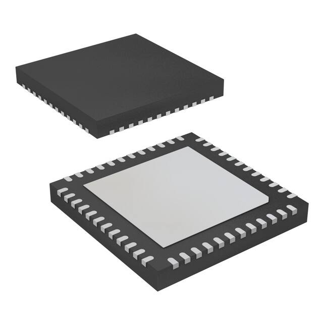


 工商网监
湘ICP备2023018690号
工商网监
湘ICP备2023018690号
