ADC78H89
www.ti.com
SNAS201D – APRIL 2003 – REVISED MARCH 2013
ADC78H89 7-Channel, 500 KSPS, 12-Bit A/D Converter
Check for Samples: ADC78H89
FEATURES
DESCRIPTION
•
•
•
•
•
The ADC78H89 is a low-power, seven-channel
CMOS 12-bit analog-to-digital converter with a
conversion throughput of 500 KSPS. The converter is
based on a successive-approximation register
architecture with an internal track-and-hold circuit. It
can be configured to accept up to seven input signals
on pins AIN1 through AIN7.
1
23
Seven Input Channels
Variable Power Management
Independent Analog and Digital Supplies
SPI™/QSPI™/MICROWIRE™/DSP Compatible
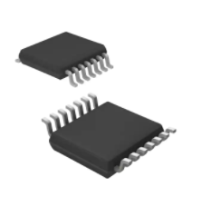
Packaged in 16-Lead TSSOP
APPLICATIONS
•
•
•
•
•
The output serial data is straight binary, and is
compatible with several standards, such as SPI™,
QSPI™, MICROWIRE™, and many common DSP
serial interfaces.
Automotive Navigation
Portable Systems
Medical Instruments
Mobile Communications
Instrumentation and Control Systems
The ADC78H89 may be operated with independent
analog and digital supplies. The analog supply (AVDD)
can range from +2.7V to +5.25V, and the digital
supply (DVDD) can range from +2.7V to AVDD. Normal
power consumption using a +3V or +5V supply is
1.5 mW and 8.3 mW, respectively. The power-down
feature reduces the power consumption to just
0.3 µW using a +3V supply, or 0.5 µW using a +5V
supply. The ADC78H89 is packaged in a 16-lead
TSSOP package. Operation over the industrial
temperature range of −40°C to +85°C is ensured.
KEY SPECIFICATIONS
•
•
•
•
Conversion Rate: 500 KSPS
DNL: ± 1 LSB (max)
INL: ± 1 LSB (max)
Power Consumption
– 3V Supply: 1.5 mW (typ)
– 5V Supply: 8.3 mW (typ)
Connection Diagram
CS
1
16
SCLK
NC
2
15
DOUT
AVDD
3
14
DIN
GND
4
13
DVDD
AIN1
5
12
GND
AIN2
6
11
AIN7
AIN3
7
10
AIN6
AIN4
8
9
AIN5
ADC78H89
Figure 1. 16-Lead TSSOP
See PW Package
1
2
3
Please be aware that an important notice concerning availability, standard warranty, and use in critical applications of
Texas Instruments semiconductor products and disclaimers thereto appears at the end of this data sheet.
TRI-STATE is a trademark of Texas Instruments.
All other trademarks are the property of their respective owners.
PRODUCTION DATA information is current as of publication date.
Products conform to specifications per the terms of the Texas
Instruments standard warranty. Production processing does not
necessarily include testing of all parameters.
Copyright © 2003–2013, Texas Instruments Incorporated
�ADC78H89
SNAS201D – APRIL 2003 – REVISED MARCH 2013
www.ti.com
These devices have limited built-in ESD protection. The leads should be shorted together or the device placed in conductive foam
during storage or handling to prevent electrostatic damage to the MOS gates.
Block Diagram
Pin Descriptions and Equivalent Circuits
Pin No.
Symbol
Equivalent Circuit
Description
ANALOG I/O
5 - 11
AIN1 to AIN7
2
NC
Analog inputs. These signals can range from 0V to AVDD.
This pin is not connected internally, and can be left floating, or tied to
ground.
DIGITAL I/O
16
SCLK
Digital clock input. The range of frequencies for this input is 50 kHz
to 8 MHz, with ensured performance at 8 MHz. This clock directly
controls the conversion and readout processes.
15
DOUT
Digital data output. The output samples are clocked out of this pin on
falling edges of the SCLK pin.
14
DIN
Digital data input. The ADC78H89's Control Register is loaded
through this pin on rising edges of the SCLK pin.
1
CS
Chip select. On the falling edge of CS, a conversion process begins.
Conversions continue as long as CS is held low.
3
AVDD
Positive analog supply pin. This pin should be connected to a quiet
+2.7V to +5.25V source and bypassed to GND with 0.1 µF ceramic
monolithic and 1 µF tantalum capacitors located within 1 cm of the
power pin.
13
DVDD
Positive digital supply pin. This pin should be connected to a +2.7V
to AVDD supply, and bypassed to GND with a 0.1 µF ceramic
monolithic capacitor located within 1 cm of the power pin.
GND
The ground return for both analog and digital supplies. These pins
are tied directly together internally, so must be connected to the
same potential. If any potential exists across these pins, large
currents will flow through the device.
POWER SUPPLY
4, 12
2
Submit Documentation Feedback
Copyright © 2003–2013, Texas Instruments Incorporated
Product Folder Links: ADC78H89
�ADC78H89
www.ti.com
SNAS201D – APRIL 2003 – REVISED MARCH 2013
ABSOLUTE MAXIMUM RATINGS
(1) (2)
Analog Supply Voltage AVDD
−0.3V to 6.5V
Digital Supply Voltage DVDD
−0.3V to AVDD + 0.3V, max 6.5V
Voltage on Any Pin to GND
−0.3V to AVDD +0.3V
(3)
±10 mA
Input Current at Any Pin
Package Input Current
(3)
±20 mA
(4)
Power Dissipation at TA = 25°C
See
ESD Susceptibility (5)
Human Body Model
Machine Model
2500V
250V
Soldering Temperature, Infrared,
10 seconds
(6)
260°C
Junction Temperature
+150°C
Storage Temperature
−65°C to +150°C
(1)
(2)
(3)
(4)
(5)
(6)
Absolute maximum ratings are limiting values which indicate limits beyond which damage to the device may occur. Operating Ratings
indicate conditions for which the device is functional, but do not ensure specific performance limits. For specifications and test
conditions, see the Electrical Characteristics. The specifications apply only for the test conditions listed. Some performance
characteristics may degrade when the device is not operated under the listed test conditions.
All voltages are measured with respect to GND = 0V, unless otherwise specified.
When the input voltage at any pin exceeds the power supplies (that is, VIN < AGND or VIN > VA or VD), the current at that pin should be
limited to 10 mA. The 50 mA maximum package input current rating limits the number of pins that can safely exceed the power supplies
with an input current of 10 mA to five.
The absolute maximum junction temperature (TJmax) for this device is 150°C. The maximum allowable power dissipation is dictated by
TJmax, the junction-to-ambient thermal resistance (θJA), and the ambient temperature (TA), and can be calculated using the formula
PDMAX = (TJmax − TA)/θJA. The values for maximum power dissipation listed above will be reached only when the ADC78H89 is
operated in a severe fault condition (e.g. when input or output pins are driven beyond the power supply voltages, or the power supply
polarity is reversed). Obviously, such conditions should always be avoided.
Human body model is 100 pF capacitor discharged through a 1.5 kΩ resistor. Machine model is 220 pF discharged through ZERO
ohms.
See http://www.ti.com/ for other methods of soldering surface mount devices.
OPERATING RATINGS
(1) (2)
−40°C ≤ TA ≤ +85°C
Operating Temperature Range
AVDD Supply Voltage
+2.7V to +5.25V
DVDD Supply Voltage
+2.7V to AVDD
Digital Input Pins Voltage Range
-0.3V to AVDD
Clock Frequency
50 kHz to 8 MHz
Analog Input Voltage
(1)
(2)
0V to AVDD
Absolute maximum ratings are limiting values which indicate limits beyond which damage to the device may occur. Operating Ratings
indicate conditions for which the device is functional, but do not ensure specific performance limits. For specifications and test
conditions, see the Electrical Characteristics. The specifications apply only for the test conditions listed. Some performance
characteristics may degrade when the device is not operated under the listed test conditions.
All voltages are measured with respect to GND = 0V, unless otherwise specified.
PACKAGE THERMAL RESISTANCE
Package
θJA
16-lead TSSOP on 4-layer, 2 oz. PCB
96°C / W
Submit Documentation Feedback
Copyright © 2003–2013, Texas Instruments Incorporated
Product Folder Links: ADC78H89
3
�ADC78H89
SNAS201D – APRIL 2003 – REVISED MARCH 2013
www.ti.com
ADC78H89 CONVERTER ELECTRICAL CHARACTERISTICS
(1)
The following specifications apply for AVDD = DVDD = +2.7V to 5.25V, fSCLK = 8 MHz, fSAMPLE = 500 KSPS unless otherwise
noted. Boldface limits apply for TA = TMIN to TMAX: all other limits TA = 25°C.
Symbol
Parameter
Conditions
Typical
Limits
Units
(2)
STATIC CONVERTER CHARACTERISTICS
Resolution with No Missing Codes
AVDD = +5.0V, DVDD = +3.3V
12
Bits
INL
Integral Non-Linearity
AVDD = +5.0V, DVDD = +3.3V
±1
LSB (max)
DNL
Differential Non-Linearity
AVDD = +5.0V, DVDD = +3.3V
±1
LSB (max)
OE
Offset Error
AVDD = +5.0V, DVDD = +3.3V
±2
LSB (max)
OEM
Offset Error Match
AVDD = +5.0V, DVDD = +3.3V
±2
LSB (max)
GE
Gain Error
AVDD = +5.0V, DVDD = +3.3V
±3
LSB (max)
GEM
Gain Error Match
AVDD = +5.0V, DVDD = +3.3V
±3
LSB (max)
DYNAMIC CONVERTER CHARACTERISTICS
SINAD
Signal-to-Noise Plus Distortion Ratio
AVDD = +5.0V, DVDD = +3.0V,
fIN = 40.2 kHz, −0.02 dBFS
72.6
dB
SNR
Signal-to-Noise Ratio
AVDD = +5.0V, DVDD = +3.0V,
fIN = 40.2 kHz, −0.02 dBFS
72.8
dB
THD
Total Harmonic Distortion
AVDD = +5.0V, DVDD = +3.0V,
fIN = 40.2 kHz, −0.02 dBFS
-86
dB
SFDR
Spurious-Free Dynamic Range
AVDD = +5.0V, DVDD = +3.0V,
fIN = 40.2 kHz, −0.02 dBFS
88
dB
ENOB
Effective Number of Bits
AVDD = +5.0V, DVDD = +3.0V,
fIN = 40.2 kHz, −0.02 dBFS
11.8
bits
Channel-to-Channel Crosstalk
AVDD = +5.0V, DVDD = +3.0V,
fIN = 40.2 kHz
-82
dB
Intermodulation Distortion, Second Order AVDD = +5.0V, DVDD = +3.0V,
Terms
fa = 40.161 kHz, fb = 41.015 kHz
-93
dB
Intermodulation Distortion, Third Order
Terms
AVDD = +5.0V, DVDD = +3.0V,
fa = 40.161 kHz, fb = 41.015 kHz
-90
dB
AVDD = +5V
11
MHz
AVDD = +3V
8
MHz
0 to
AVDD
V
IMD
FPBW
-3 dB Full Power Bandwidth
ANALOG INPUT CHARACTERISTICS
VIN
Input Range
IDCL
DC Leakage Current
CINA
Input Capacitance
±1
µA (max)
In Track Mode
33
pF
In Hold Mode
3
pF
DIGITAL INPUT CHARACTERISTICS
DVDD = +4.75Vto +5.25V
2.4
V (min)
DVDD = +2.7V to +3.6V
2.1
V (min)
VIH
Input High Voltage
VIL
Input Low Voltage
DVDD = +2.7V to +5.25V
IIN
Input Current
VIN = 0V or DVDD
CIND
Input Capacitance
0.8
V (max)
±0.01
1
µA (max)
2
4
pF (max)
DVDD −0.5
V (min)
0.4
V (max)
±1
µA (max)
4
pF (max)
DIGITAL OUTPUT CHARACTERISTICS
VOH
Output High Voltage
ISOURCE = 200 µA,
DVDD = +2.7V to +5.25V
VOL
Output Low Voltage
ISINK = 200 µA
IOZH, IOZL TRI-STATE Leakage Current
COUT
TRI-STATE Output Capacitance
2
Output Coding
(1)
(2)
4
Straight (Natural) Binary
Data sheet min/max specification limits are specified by design, test, or statistical analysis.
Tested limits are specified to AOQL (Average Outgoing Quality Level).
Submit Documentation Feedback
Copyright © 2003–2013, Texas Instruments Incorporated
Product Folder Links: ADC78H89
�ADC78H89
www.ti.com
SNAS201D – APRIL 2003 – REVISED MARCH 2013
ADC78H89 CONVERTER ELECTRICAL CHARACTERISTICS (1) (continued)
The following specifications apply for AVDD = DVDD = +2.7V to 5.25V, fSCLK = 8 MHz, fSAMPLE = 500 KSPS unless otherwise
noted. Boldface limits apply for TA = TMIN to TMAX: all other limits TA = 25°C.
Symbol
Parameter
Conditions
POWER SUPPLY CHARACTERISTICS (CL = 10 pF)
AVDD,
DVDD
Typical
Limits
Units
(2)
(3)
AVDD ≥ DVDD
Analog and Digital Supply Voltages
2.7
V (min)
5.25
V (max)
AVDD = DVDD = +4.75V to +5.25V,
fSAMPLE = 500 KSPS, fIN = 40 kHz
1.65
2.3
mA (max)
AVDD = DVDD = +2.7V to +3.6V,
fSAMPLE = 500 KSPS, fIN = 40 kHz
0.5
2.3
mA (max)
AVDD = DVDD = +4.75V to +5.25V,
fSAMPLE = 0 KSPS
0.1
µA
AVDD = DVDD = +2.7V to +3.6V,
fSAMPLE = 0 KSPS
0.1
µA
Power Consumption, Normal Mode
(Operational, CS low)
AVDD = DVDD = +4.75V to +5.25V
8.3
12
mW (max)
AVDD = DVDD = +2.7V to +3.6V
1.5
8.3
mW (max)
Power Consumption, Shutdown (CS
high)
AVDD = DVDD = +4.75V to +5.25V
0.5
µW
AVDD = DVDD = +2.7V to +3.6V
0.3
µW
Total Supply Current, Normal Mode
(Operational, CS low)
IDD
Total Supply Current, Shutdown (CS
high)
PD
AC ELECTRICAL CHARACTERISTICS
fSCLK
Maximum Clock Frequency
8
Minimum Clock Frequency
fS
Maximum Sample Rate
tCONV
Conversion Time
13
DC
Duty Cycle
50
tACQ
Track/Hold Acquisition Time
Full-Scale Step Input
Throughput Time
Conversion Time + Acquisition Time
fRATE
Throughput Rate
tAD
Aperture Delay
(3)
MHz (max)
50
kHz
500
KSPS (min)
13
SCLK cycles
40
% (min)
60
% (max)
3
SCLK cycles
16
SCLK cycles
500
KSPS (min)
4
ns
Except power supply pins.
ADC78H89 TIMING SPECIFICATIONS
The following specifications apply for AVDD = DVDD = +2.7V to 5.25V, fSCLK = 8 MHz, CL = 50 pF, Boldface limits apply for
TA = TMIN to TMAX: all other limits TA = 25°C.
Symbol
(1)
Parameter
Conditions
Typical
Limits
Units
10
ns (min)
10
ns (min)
t1a
SCLK High to CS Fall Setup Time
See
(1)
t1b
SCLK Low to CS Fall Hold Time
See
(1)
t2
Delay from CS Until DOUT TRI-STATE™ Disabled
30
ns (max)
t3
Data Access Time after SCLK Falling Edge
30
ns (max)
t4
Data Setup Time Prior to SCLK Rising Edge
10
ns (max)
t5
Data Valid SCLK Hold Time
10
ns (max)
t6
SCLK High Pulse Width
0.4 x tSCLK
ns (min)
t7
SCLK Low Pulse Width
0.4 x tSCLK
ns (min)
t8
CS Rising Edge to DOUT High-Impedance
20
ns (max)
Clock may be in any state (high or low) when CS is asserted, with the restrictions on setup and hold time given by t1a and t1b.
Submit Documentation Feedback
Copyright © 2003–2013, Texas Instruments Incorporated
Product Folder Links: ADC78H89
5
�ADC78H89
SNAS201D – APRIL 2003 – REVISED MARCH 2013
www.ti.com
Timing Diagrams
Figure 2. ADC78H89 Operational Timing Diagram
Figure 3. Timing Test Circuit
CS
tCONVERT
tACQ
t6
SCLK
1
2
3
4
Z3
Z2
Z1
7
8
16
t8
t3
Z0
DB11
DB10
DB9
DB8
DB1
DB0
t5
t4
DIN
6
t7
t2
DOUT
5
DONT DONTC ADD2
ADD1
ADD0 DONTC DONTC DONTC
Figure 4. ADC78H89 Serial Timing Diagram
Figure 5. SCLK and CS Timing Parameters
6
Submit Documentation Feedback
Copyright © 2003–2013, Texas Instruments Incorporated
Product Folder Links: ADC78H89
�ADC78H89
www.ti.com
SNAS201D – APRIL 2003 – REVISED MARCH 2013
Specification Definitions
ACQUISITION TIME is the time required to acquire the input voltage. That is, it is time required for the hold
capacitor to charge up to the input voltage.
APERTURE DELAY is the time between the fourth falling SCLK edge of a conversion and the time when the
input signal is acquired or held for conversion.
CONVERSION TIME is the time required, after the input voltage is acquired, for the ADC to convert the input
voltage to a digital word.
CROSSTALK is the coupling of energy from one channel into the other channel, or the amount of signal energy
from one analog input that appears at the measured analog input.
DIFFERENTIAL NON-LINEARITY (DNL) is the measure of the maximum deviation from the ideal step size of 1
LSB.
DUTY CYCLE is the ratio of the time that a repetitive digital waveform is high to the total time of one period. The
specification here refers to the SCLK.
EFFECTIVE NUMBER OF BITS (ENOB, or EFFECTIVE BITS) is another method of specifying Signal-to-Noise
and Distortion or SINAD. ENOB is defined as (SINAD - 1.76) / 6.02 and says that the converter is equivalent to a
perfect ADC of this (ENOB) number of bits.
FULL POWER BANDWIDTH is a measure of the frequency at which the reconstructed output fundamental
drops 3 dB below its low frequency value for a full scale input.
GAIN ERROR is the deviation of the last code transition (111...110) to (111...111) from the ideal (VREF - 1.5
LSB), after adjusting for offset error.
INTEGRAL NON-LINEARITY (INL) is a measure of the deviation of each individual code from a line drawn from
negative full scale (½ LSB below the first code transition) through positive full scale (½ LSB above the last code
transition). The deviation of any given code from this straight line is measured from the center of that code value.
INTERMODULATION DISTORTION (IMD) is the creation of additional spectral components as a result of two
sinusoidal frequencies being applied to the ADC input at the same time. It is defined as the ratio of the power in
the both second order (or all four third order) intermodulation products to the sum of the power in both of the
original frequencies. IMD is usually expressed in dBFS.
MISSING CODES are those output codes that will never appear at the ADC outputs. The ADC78H89 is ensured
not to have any missing codes.
OFFSET ERROR is the deviation of the first code transition (000...000) to (000...001) from the ideal (i.e. GND +
0.5 LSB).
SIGNAL TO NOISE RATIO (SNR) is the ratio, expressed in dB, of the rms value of the input signal to the rms
value of the sum of all other spectral components below one-half the sampling frequency, not including
harmonics or d.c.
SIGNAL TO NOISE PLUS DISTORTION (S/N+D or SINAD) Is the ratio, expressed in dB, of the rms value of the
input signal to the rms value of all of the other spectral components below half the clock frequency, including
harmonics but excluding d.c.
SPURIOUS FREE DYNAMIC RANGE (SFDR) is the difference, expressed in dB, between the rms values of the
input signal and the peak spurious signal, where a spurious signal is any signal present in the output spectrum
that is not present at the input.
TOTAL HARMONIC DISTORTION (THD) is the ratio, expressed in dB, expressed in dB or dBc, of the rms total
of the first five harmonic components at the output to the rms level of the input signal frequency as seen at the
output. THD is calculated as
THD = 20 ‡ log10
A f 22 +
+ A f 62
A f 12
(1)
where Af1 is the RMS power of the input frequency at the output and Af2 through Af6 are the RMS power in the
first 5 harmonic frequencies.
Submit Documentation Feedback
Copyright © 2003–2013, Texas Instruments Incorporated
Product Folder Links: ADC78H89
7
�ADC78H89
SNAS201D – APRIL 2003 – REVISED MARCH 2013
www.ti.com
THROUGHPUT TIME is the minimum time required between the start of two successive conversion. It is the
acquisition time plus the conversion time. In the case of the ADC78H89, this is 16 SCLK periods.
8
Submit Documentation Feedback
Copyright © 2003–2013, Texas Instruments Incorporated
Product Folder Links: ADC78H89
�ADC78H89
www.ti.com
SNAS201D – APRIL 2003 – REVISED MARCH 2013
TYPICAL PERFORMANCE CHARACTERISTICS
TA = +25°C, fSAMPLE = 500 KSPS, fSCLK = 8 MHz, fIN = 40.2 kHz unless otherwise stated.
DNL
DNL
Figure 6.
Figure 7.
INL
INL
Figure 8.
Figure 9.
DNL vs. Supply
INL vs. Supply
Figure 10.
Figure 11.
Submit Documentation Feedback
Copyright © 2003–2013, Texas Instruments Incorporated
Product Folder Links: ADC78H89
9
�ADC78H89
SNAS201D – APRIL 2003 – REVISED MARCH 2013
www.ti.com
TYPICAL PERFORMANCE CHARACTERISTICS (continued)
TA = +25°C, fSAMPLE = 500 KSPS, fSCLK = 8 MHz, fIN = 40.2 kHz unless otherwise stated.
10
SNR vs. Supply
THD vs. Supply
Figure 12.
Figure 13.
ENOB vs. Supply
SNR vs. Input Frequency
Figure 14.
Figure 15.
THD vs. Input Frequency
ENOB vs. Input Frequency
Figure 16.
Figure 17.
Submit Documentation Feedback
Copyright © 2003–2013, Texas Instruments Incorporated
Product Folder Links: ADC78H89
�ADC78H89
www.ti.com
SNAS201D – APRIL 2003 – REVISED MARCH 2013
TYPICAL PERFORMANCE CHARACTERISTICS (continued)
TA = +25°C, fSAMPLE = 500 KSPS, fSCLK = 8 MHz, fIN = 40.2 kHz unless otherwise stated.
Spectral Response
Spectral Response
Figure 18.
Figure 19.
Power Consumption vs. Throughput
Figure 20.
Submit Documentation Feedback
Copyright © 2003–2013, Texas Instruments Incorporated
Product Folder Links: ADC78H89
11
�ADC78H89
SNAS201D – APRIL 2003 – REVISED MARCH 2013
www.ti.com
APPLICATION INFORMATION
USING THE ADC78H89
An operational timing diagram and a serial interface timing diagram for the ADC78H89 are shown in the Timing
Diagrams section. CS is chip select, which initiates conversions and frames the serial data transfers. SCLK
(serial clock) controls both the conversion process and the timing of serial data. DOUT is the serial data output
pin, where a conversion result is sent as a serial data stream, MSB first. Data to be written to the ADC78H89's
Control Register is placed on DIN, the serial data in pin.
The conversion process and serial data timing are controlled by the SCLK. Each conversion requires 16 SCLK
cycles to complete. Conversions are begun by bringing CS low. Several conversions can be executed
sequentially in a single serial frame, which is defined as the time between falling and rising edges of CS. If CS is
held low continuously, the ADC78H89 will perform conversions continuously.
Each time CS goes low, a conversion process is initiated simultaneously with a load of the Control Register. The
new contents of the Control Register will affect the next conversion. There is thus a one sample delay between
selecting a new input channel and observing the corresponding output.
Basic operation of the ADC78H89 begins with CS going low and initiating a conversion process and data
transfer. At this time the DOUT pin comes out of the high impedance state. The converter enters track mode at
the first falling edge of SCLK after CS is brought low, and begins to acquire the input signal. Acquisition of the
input signal continues during the first three SCLK cycles after the falling edge of CS. This acquisition time is
denoted by tACQ. The converter goes from track to hold mode on the fourth falling edge of SCLK, and the analog
input signal is sampled at this time (see Figure 2).
The ADC78H89 supports idling SCLK either high or low between conversions, when CS is high. The SCLK may
also run continuously while CS is high. Regardless of whether the clock is idled, SCLK is internally gated off
when CS is brought high. If SCLK is in the low state when CS goes high, the subsequent fall of CS will generate
a falling edge of the internal version of SCLK, putting the ADC into the track mode. This is seen as the first falling
edge of SCLK. If SCLK is in the high state when CS goes high, the ADC enters the track mode on the first falling
edge of SCLK after the falling edge of CS (see Figure 2). In both cases, a total of sixteen falling edges are
required to complete the acquisition and conversion process.
Sixteen SCLK cycles are required to read a complete sample from the ADC78H89. Each bit of the sample
(including leading zeros) is valid on subsequent rising edges of SCLK. The ADC78H89 will produce four leading
zeros on DOUT, followed by twelve data bits, most significant first. The final data bit, DB0, will be clocked out on
the 16th SCLK falling edge, and will be valid on the following rising edge. Depending upon the application, the
first edge on SCLK after CS goes low may be either a falling edge or a rising edge. If the first SCLK edge after
CS goes low is a falling edge, all four leading zeros will be valid on the first four rising edges of SCLK. If the first
SCLK edge after CS goes low is a rising edge, the first leading zero may not be set up in time for a
microprocessor or DSP to read it correctly. The remaining data bits are still clocked out on the falling edges of
SCLK, so that they are valid on the rising edges of SCLK.
Control information must be written to the Control Register whenever a conversion is performed. Information is
written to the Control Register on the first eight rising edges of SCLK of each conversion. It is important that the
DIN line is set up with the correct information when reading data from the ADC78H89. The input channel to be
sampled in the next conversion process is determined by writing information to the Control Register in the current
conversion.
On the rising edges of SCLK after CS is brought low, data is loaded through the DIN pin to the Control Register,
MSB first. Since the data on the DIN pin is transferred while the conversion data is being read, 16 serial clocks
are required for each data transfer. The control register only loads the information on the first 8 rising SCLK
edges; DIN is ignored for the last 8 rising edges. Table 1 describes the bit functions, where MSB indicates the
first bit of information in the loaded data. At power-up, the control register defaults to all zeros in the bit locations.
Table 1. Control Register Bits
12
Bit 7 (MSB)
Bit 6
Bit 5
Bit 4
Bit 3
Bit 2
Bit 1
Bit 0
DONTC
DONTC
ADD2
ADD1
ADD0
DONTC
DONTC
DONTC
Submit Documentation Feedback
Copyright © 2003–2013, Texas Instruments Incorporated
Product Folder Links: ADC78H89
�ADC78H89
www.ti.com
SNAS201D – APRIL 2003 – REVISED MARCH 2013
Table 2. Control Register Bit Descriptions
Bit #:
Symbol:
Description
7, 6, 2, 1, 0
DONTC
Don't care. The value of this bit does not affect the device.
5
ADD2
4
ADD1
These three bits determine which input channel will be sampled and converted on the next falling edge of CS.
The mapping between codes and channels is shown in Table 3.
3
ADD0
Table 3. Input Channel Selection
ADD2
ADD1
ADD0
Input Channel
0
0
0
AIN1 (Default)
0
0
1
AIN2
0
1
0
AIN3
0
1
1
AIN4
1
0
0
AIN5
1
0
1
AIN6
1
1
0
AIN7
1
1
1
GND
ADC78H89 OPERATION
The ADC78H89 is a successive-approximation analog-to-digital converter designed around a chargeredistribution digital-to-analog converter. Simplified schematics of the ADC78H89 in both track and hold modes
are shown in Figure 21 and Figure 22, respectively. In Figure 21, the ADC78H89 is in track mode: switch SW1
connects the sampling capacitor to one of seven analog input channels through the multiplexer, and SW2
balances the comparator inputs. The ADC78H89 is in this state for the first three SCLK cycles after CS is
brought low.
The user does not need to worry about any kind of power-up delays or dummy conversions with the ADC78H89.
The part is able to acquire input to full resolution in the first conversion immediately following power-up. The first
conversion after power up will be that of the first channel.
Figure 22 shows the ADC78H89 in hold mode: switch SW1 connects the sampling capacitor to ground,
maintaining the sampled voltage, and switch SW2 unbalances the comparator. The control logic then instructs
the charge-redistribution DAC to add or subtract fixed amounts of charge from the sampling capacitor until the
comparator is balanced. When the comparator is balanced, the digital word supplied to the DAC is the digital
representation of the analog input voltage. The ADC78H89 is in this state for the last thirteen SCLK cycles after
CS is brought low.
Figure 21. ADC78H89 in Track Mode
Submit Documentation Feedback
Copyright © 2003–2013, Texas Instruments Incorporated
Product Folder Links: ADC78H89
13
�ADC78H89
SNAS201D – APRIL 2003 – REVISED MARCH 2013
www.ti.com
Figure 22. ADC78H89 in Hold Mode
ADC78H89 TRANSFER FUNCTION
The output format of the ADC89H89 is straight binary. Code transitions occur midway between successive
integer LSB values. The LSB width for the ADC78H89 is AVDD / 4096. The ideal transfer characteristic is shown
in Figure 23.
Figure 23. Ideal Transfer Characteristic
TYPICAL APPLICATION CIRCUIT
A typical application of the ADC78H89 is shown in Figure 24. The split analog and digital supplies are both
provided in this example by the Texas Instruments LP2950 low-dropout voltage regulator, available in a variety of
fixed and adjustable output voltages. The analog supply is bypassed with a capacitor network located close to
the ADC78H89. The digital supply is separated from the analog supply by an isolation resistor and conditioned
with additional bypass capacitors. The ADC78H89 uses the analog supply (AVDD) as its reference voltage, so it
is very important that AVDD be kept as clean as possible. Because of the ADC78H89's low power requirements, it
is also possible to use a precision reference as a power supply to maximize performance. The four-wire interface
is also shown connected to a microprocessor or DSP.
14
Submit Documentation Feedback
Copyright © 2003–2013, Texas Instruments Incorporated
Product Folder Links: ADC78H89
�ADC78H89
www.ti.com
SNAS201D – APRIL 2003 – REVISED MARCH 2013
Figure 24. Typical Application Circuit
ANALOG INPUTS
An equivalent circuit for one of the ADC78H89's input channels is shown in Figure 25. At the start of each
conversion, one of the ADC78H89's seven channels are selected. Diodes D1 and D2 provide ESD protection for
the analog inputs. At no time should an analog input be beyond (AVDD + 300 mV) or (GND - 300 mV), as these
ESD diodes will begin conducting, which could cause erratic operation.
The capacitor C1 in Figure 25 typically has a value of 3 pF, and is mainly the package pin capacitance. Resistor
R1 is the on resistance of the multiplexer and track / hold switch, and is typically 500 ohms. Capacitor C2 is the
ADC78H89 sampling capacitor, and is typically 30 pF. The ADC78H89 will deliver best performance when driven
by a low-impedance source to eliminate distortion caused by the charging of the sampling capacitor.
Figure 25. Equivalent Input Circuit
In applications where dynamic performance is critical, the ADC78H89 might need to be driven with a low outputimpedance amplifier. In addition, when using the ADC78H89 to sample AC signals, a band-pass or low-pass filter
will reduce harmonics and noise, improving dynamic performance.
DIGITAL INPUTS AND OUTPUTS
The ADC78H89's digital inputs (SCLK, CS, and DIN) are limited by and cannot exceed the analog supply voltage
AVDD. The digital input pins are not prone to latch-up; SCLK, CS, and DIN may be asserted before DVDD without
any risk.
POWER SUPPLY CONSIDERATIONS
The ADC78H89 has two supplies, although they could both have the same potential. There are two major power
supply concerns with this product. They are relative power supply levels, including power-on sequencing, and the
effect of digital supply noise on the analog supply.
Power Management
The ADC78H89 is a dual-supply device. These two supplies share ESD resources, and thus care must be
exercised to ensure that the power supplies are applied in the correct sequence. To avoid turning on the ESD
diodes, the digital supply (DVDD) cannot exceed the analog supply (AVDD) by more than 300 mV. The
ADC78H89's analog power supply must, therefore, be applied before (or concurrently with) the digital power
supply.
Submit Documentation Feedback
Copyright © 2003–2013, Texas Instruments Incorporated
Product Folder Links: ADC78H89
15
�ADC78H89
SNAS201D – APRIL 2003 – REVISED MARCH 2013
www.ti.com
The ADC78H89 is fully powered-up whenever CS is low, and fully powered-down whenever CS is high, with one
exception: the ADC78H89 automatically enters power-down mode between the 16th falling edge of a conversion
and the 1st falling edge of the subsequent conversion (see Figure 2).
The ADC78H89 can perform multiple conversions back to back; each conversion requires 16 SCLK cycles. The
ADC78H89 will perform conversions continuously as long as CS is held low.
The user may trade off throughput for power consumption by simply performing fewer conversions per unit time.
The Power Consumption vs. Sample Rate curve in the Typical Performance Curves section shows the typical
power consumption of the ADC78H89 versus throughput. To calculate the power consumption, simply multiply
the fraction of time spent in the normal mode by the normal mode power consumption (8.3 mW with AVDD =
DVDD = +3.6V, for example), and add the fraction of time spent in shutdown mode multiplied by the shutdown
mode power dissipation (0.3 mW with AVDD = DVDD = +3.6V).
Power Supply Noise Considerations
The charging of any output load capacitance requires current from the digital supply, DVDD. The current pulses
required from the supply to charge the output capacitance will cause voltage variations on the digital supply. If
these variations are large enough, they could cause degrade SNR and SINAD performance of the ADC.
Furthermore, if the analog and digital supplies are tied directly together, the noise on the digital supply will be
coupled directly into the analog supply, causing greater performance degradation than noise on the digital
supply. Furthermore, discharging the output capacitance when the digital output goes from a logic high to a logic
low will dump current into the die substrate, which is resistive. Load discharge currents will cause "ground
bounce" noise in the substrate that will degrade noise performance if that current is large enough. The larger is
the output capacitance, the more current flows through the die substrate and the greater is the noise coupled into
the analog channel, degrading noise performance.
The first solution is to decouple the analog and digital supplies from each other, or use separate supplies for
them, to keep digital noise out of the analog supply. To keep noise out of the digital supply, keep the output load
capacitance as small as practical. If the load capacitance is greater than 25 pF, use a 100 Ω series resistor at
the ADC output, located as close to the ADC output pin as practical. This will limit the charge and discharge
current of the output capacitance and improve noise performance.
16
Submit Documentation Feedback
Copyright © 2003–2013, Texas Instruments Incorporated
Product Folder Links: ADC78H89
�ADC78H89
www.ti.com
SNAS201D – APRIL 2003 – REVISED MARCH 2013
REVISION HISTORY
Changes from Revision C (March 2013) to Revision D
•
Page
Changed layout of National Data Sheet to TI format .......................................................................................................... 16
Submit Documentation Feedback
Copyright © 2003–2013, Texas Instruments Incorporated
Product Folder Links: ADC78H89
17
�PACKAGE OPTION ADDENDUM
www.ti.com
6-Feb-2020
PACKAGING INFORMATION
Orderable Device
Status
(1)
Package Type Package Pins Package
Drawing
Qty
Eco Plan
Lead/Ball Finish
MSL Peak Temp
(2)
(6)
(3)
Op Temp (°C)
Device Marking
(4/5)
ADC78H89CIMT/NOPB
ACTIVE
TSSOP
PW
16
92
Green (RoHS
& no Sb/Br)
SN
Level-1-260C-UNLIM
-40 to 85
78H89
CIMT
ADC78H89CIMTX/NOPB
ACTIVE
TSSOP
PW
16
2500
Green (RoHS
& no Sb/Br)
SN
Level-1-260C-UNLIM
-40 to 85
78H89
CIMT
(1)
The marketing status values are defined as follows:
ACTIVE: Product device recommended for new designs.
LIFEBUY: TI has announced that the device will be discontinued, and a lifetime-buy period is in effect.
NRND: Not recommended for new designs. Device is in production to support existing customers, but TI does not recommend using this part in a new design.
PREVIEW: Device has been announced but is not in production. Samples may or may not be available.
OBSOLETE: TI has discontinued the production of the device.
(2)
RoHS: TI defines "RoHS" to mean semiconductor products that are compliant with the current EU RoHS requirements for all 10 RoHS substances, including the requirement that RoHS substance
do not exceed 0.1% by weight in homogeneous materials. Where designed to be soldered at high temperatures, "RoHS" products are suitable for use in specified lead-free processes. TI may
reference these types of products as "Pb-Free".
RoHS Exempt: TI defines "RoHS Exempt" to mean products that contain lead but are compliant with EU RoHS pursuant to a specific EU RoHS exemption.
Green: TI defines "Green" to mean the content of Chlorine (Cl) and Bromine (Br) based flame retardants meet JS709B low halogen requirements of