User's Guide
SBAU297 – October 2017
ADS1x2C04 Evaluation Module
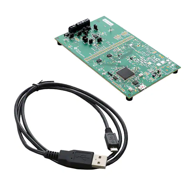
Figure 1. ADS1x2C04 Evaluation Module (ADS122C04EVM Shown)
The ADS1x2C04EVM is an evaluation module kit that provides hardware and software support for
evaluation of the devices in the ADS122C04 family. The ADS122C04 is a 24-bit delta-sigma analog-todigital converter (ADC). The kit utilizes the TM4C1294NCPDT processor to communicate with the ADC via
I2C and provide communication with a PC over USB interface. The kit also includes a software application
that runs on a PC allowing for register manipulation and data collection from the ADC. The
ADS1x2C04EVM kit includes the ADS1x2C04 device along with a USB micro cable, and downloadable
supporting software (SW).
This document includes a detailed description of the hardware (HW), software, bill of materials (BOM),
and schematic for the ADS1x2C04EVM.
Throughout this document the term EVM is synonymous with ADS1x2C04EVM, demonstration kit, and
evaluation module. The term ADS1x2C04EVM is a generic name that applies to any EVM in the
ADS122C04 device family. Specifically, the ADS122C04EVM uses the ADS122C04 as the main device on
the EVM. The term GUI is synonymous with Delta-Sigma ADC EvaluaTIon Software, core application, and
EVM software. The use of Tiva™ is synonymous with the TM4C1294NCPDT microcontroller.
Table 1. Related Documentation
Device
Literature Number
ADS122C04
SBAS751
SBAU297 – October 2017
Submit Documentation Feedback
ADS1x2C04 Evaluation Module
Copyright © 2017, Texas Instruments Incorporated
1
�www.ti.com
1
2
3
4
5
6
7
Contents
EVM Overview ............................................................................................................... 4
1.1
Description ........................................................................................................... 4
1.2
Requirements ....................................................................................................... 4
1.3
Software Reference ................................................................................................ 4
1.4
Supported Functionality ............................................................................................ 4
Quick Start .................................................................................................................... 5
2.1
Default Jumper and Switch Configuration ....................................................................... 5
2.2
Power Connection .................................................................................................. 6
2.3
Startup................................................................................................................ 6
Hardware Reference ........................................................................................................ 6
3.1
Jumper and Switch Configuration Reference ................................................................... 6
3.2
Header, Connector and Test Point Reference ................................................................ 10
Software Details ............................................................................................................ 12
4.1
Installing the Software ............................................................................................ 12
4.2
Connecting to the EVM Hardware .............................................................................. 13
4.3
Using the Software With the ADS1x2C04EVM ................................................................ 14
EVM Hardware Details .................................................................................................... 23
5.1
Analog Inputs ...................................................................................................... 23
5.2
Digital Inputs ....................................................................................................... 30
5.3
ADC Reference .................................................................................................... 31
5.4
Reset ................................................................................................................ 32
Power Supply Connections – EVM and ADC .......................................................................... 33
6.1
Powering the EVM ................................................................................................ 33
6.2
Powering the ADS1x2C04 ....................................................................................... 33
ADS1x2C04 Bill of Materials, PCB Layouts, and Schematics........................................................ 34
7.1
Bill of Materials .................................................................................................... 34
7.2
PCB Layouts ....................................................................................................... 39
7.3
Schematic .......................................................................................................... 42
List of Figures
1
ADS1x2C04 Evaluation Module (ADS122C04EVM Shown) ........................................................... 1
2
ADS1x2C04 EVM ............................................................................................................ 6
3
Input Terminal Blocks ...................................................................................................... 10
4
Delta-Sigma Evaluation Engine Installation Instructions .............................................................. 12
5
ADS1x2C04 Device Package Installation Instructions (ADS122C04 Shown)...................................... 13
6
ADS1x2C04 Device Tab (ADS122C04 Shown) ........................................................................ 14
7
ADS1x2C04 Input MUX Config 0 Register (ADS122C04 Shown) ................................................... 15
8
ADS1x2C04 Input MUX Selection (ADS122C04 Shown) ............................................................. 16
9
Data Inspector .............................................................................................................. 17
10
Time Domain................................................................................................................ 17
11
Histogram
12
13
14
15
16
17
18
19
20
21
2
...................................................................................................................
Data Displayed as HEX Values ..........................................................................................
Data Displayed as Decimal Values ......................................................................................
3-Wire RTD Predefined Script ............................................................................................
3-Wire RTD Script Detail ..................................................................................................
Simplified 3-Wire RTD Input Diagram ...................................................................................
Simplified 2-Wire RTD Input Diagram ...................................................................................
Simplified 4-Wire RTD Input Diagram ...................................................................................
Simplified Thermocouple Input Diagram (J6) ...........................................................................
Simplified Bridge Input Diagram..........................................................................................
Simplified Voltage and Current Input Diagram .........................................................................
ADS1x2C04 Evaluation Module
18
18
19
21
22
24
25
26
27
28
30
SBAU297 – October 2017
Submit Documentation Feedback
Copyright © 2017, Texas Instruments Incorporated
�www.ti.com
22
Simplified External REF Input ............................................................................................ 31
23
Top Silkscreen .............................................................................................................. 39
24
Top Layer (Positive)
39
25
Ground Layer (Negative)
40
26
27
28
29
30
31
32
33
34
.......................................................................................................
.................................................................................................
Power Layer (Negative) ..................................................................................................
Bottom Layer (Positive)....................................................................................................
Bottom Silkscreen .........................................................................................................
ADS1x2C04EVM ADC Schematic .......................................................................................
ADS1x2C04EVM Controller Schematic .................................................................................
ADS1x2C04EVM Controller Power Schematic .........................................................................
ADS1x2C04EVM Digital Header Schematic ............................................................................
ADS1x2C04EVM Power USB Schematic ...............................................................................
ADS1x2C04EVM Power External Schematic...........................................................................
40
41
41
42
43
44
45
46
47
Trademarks
Tiva is a trademark of Texas Instruments.
Microsoft, Windows are registered trademarks of Microsoft Corporation.
SBAU297 – October 2017
Submit Documentation Feedback
ADS1x2C04 Evaluation Module
Copyright © 2017, Texas Instruments Incorporated
3
�EVM Overview
1
EVM Overview
1.1
Description
www.ti.com
This user guide describes the operation and use of the ADS1x2C04 evaluation module. One example is
the ADS122C04EVM. The ADS122C04 is a 24-bit, 2-kSPS, 4-channel delta-sigma analog-to-digital
converter (ADC) for precision sensor measurement applications. The ADS1x2C04EVM platform is
intended for evaluating the ADS122C04 device family for performance and functionality.
1.2
Requirements
1.2.1
Software Requirements
PC with Microsoft® Windows® 7 or higher operating system.
1.2.2
Hardware Requirements
PC with available USB 2.0 or greater connection.
1.2.2.1
Power Supply
USB powered.
1.3
Software Reference
Refer to Delta-Sigma ADC EvaluaTIon Software User Manual for the core software documentation or
navigate to the File -> About option from within the GUI, then click on the Software user guide icon.
1.4
Supported Functionality
1.4.1
•
•
•
•
•
Supported Hardware Functionality
Unipolar (3.3 V or 5 V) AVDD and AVSS (GND) supply operation
3.3-V DVDD
Digital header for external processor or controller configuration
Configurable for direct sensor input
Onboard 2.5-V reference or user-supplied external ADC voltage reference
•
•
•
•
•
•
•
Supported Software Functionality
Start and sync control
Device software reset
Device powerdown
Device configuration register read and write
Conversion result readback
Missed conversion detection through data conversion result counter information
Data integrity check by CRC of data or by inverted conversion result
1.4.2
4
ADS1x2C04 Evaluation Module
SBAU297 – October 2017
Submit Documentation Feedback
Copyright © 2017, Texas Instruments Incorporated
�Quick Start
www.ti.com
2
Quick Start
This section provides a guide to quickly begin using the EVM.
2.1
Default Jumper and Switch Configuration
The EVM should come configured with the settings listed in Table 2 and illustrated in Figure 2.
Table 2. Default Settings
Jumper
Position
JP1
Not Installed
Use onboard processor
JP2
Not Installed
USB-derived supplies ON
JP3
Not Installed
DVDD from USB supply (1-2 connection via R83)
JP4
Not Installed
AVDD from USB supply (1-2 connection via R84)
JP5
Not Installed
N/A
JP6
(1)
Excitation source connected to IDAC using REFP
JP7
Not Installed
A0 address selection (default to GND through resistor R57)
JP8
Not Installed
A1 address selection (default to GND through resistor R60)
JP9
(1)
1-2
J6 pin 5 connected to excitation source
JP10
Not Installed
JP11 (1)
1-2
JP12
Not Installed
Weak pullup to AVDD not connected to AIN1
Not Installed
Weak pulldown to GND not connected to AIN2
JP13
(1)
1-2
Function
(1)
AIN0 not connected to input voltage divider
AVDD supply sourced from 5 V
JP14 (1)
2-3
JP15
Installed
DVDD supply connected
AVDD supply connected
JP16
Installed
JP17 (1)
1-2
JP18 (1)
Not Installed
Switch
Position
S5
Down
RTD bias pedestal connected
VREF is supplied by the 2.5-V onboard reference (U24)
COM connected to GND (2-3 connection via R90)
Function
External reference connected to JP6
Pin 1 is identified with a dot on the PCB silkscreen.
SBAU297 – October 2017
Submit Documentation Feedback
ADS1x2C04 Evaluation Module
Copyright © 2017, Texas Instruments Incorporated
5
�Quick Start
www.ti.com
Figure 2. ADS1x2C04 EVM
2.2
Power Connection
The EVM is powered through the USB interface with the PC. Connect the EVM to a USB connector on the
PC to power the board.
2.3
Startup
Use the following steps at startup:
1. Install the core application software on the PC.
2. Install the device software on the PC. (For example, ADS122C04 Device Package for the
ADS122C04EVM.)
3. Ensure all jumpers and switches are configured in the default configuration per Table 2 and Figure 2.
4. Connect the EVM to the PC using a USB cable.
5. If prompted, install any required drivers.
6. Start the GUI software on your PC.
NOTE: The device has powered correctly if D1 and D4 are both lit green.
3
Hardware Reference
3.1
Jumper and Switch Configuration Reference
Table 3 provides all jumper and switch configuration settings for the EVM.
6
ADS1x2C04 Evaluation Module
SBAU297 – October 2017
Submit Documentation Feedback
Copyright © 2017, Texas Instruments Incorporated
�Hardware Reference
www.ti.com
Table 3. Jumper and Switch Options
Jumper
JP1
JP2
JP3
JP4
JP5
JP6(1)
JP7
JP8
JP9(1)
JP10
JP11(1)
JP12
Position
Description
Operation of EVM with external digital signals
Installed (ON)
Hold Tiva processor (U1) in reset and disable level shifters to allow external digital
signals
Uninstalled (OFF)
Normal operation with onboard Tiva processor (default)
Power down USB power supplies
Installed (ON)
USB-derived power supplies disabled and powered down
Uninstalled (OFF)
USB-derived power supplies enabled and ON (default)
Digital supply source
1-2 shorted
Provided from USB power (default using R83 as the short)
2-3 shorted
External supply source
Open
No digital system power provided
Analog supply source
1-2 shorted
Provided from USB power (default using R84 as the short)
2-3 shorted
External supply source
Open
No analog system power provided
External 5-V power down
Installed (ON)
External supply regulator (U16) disabled and powered down
Uninstalled (OFF)
External supply regulator (U16) enabled and ON (default)
AIN0 input connection (U23)
1-2 shorted
Current excitation possible when S5 is in the down position to JP6 (default)
2-3 shorted
Voltage excitation through AVDD
Open
Not connected to an excitation source
2
I C A0 address selection (not installed)
1-2 shorted
DVDD
3-4 shorted
GND (default through R57)
5-6 shorted
SCL
7-8 shorted
SDA
Open
(input floating)
I2C A1 address selection (not installed)
1-2 shorted
DVDD
3-4 shorted
GND (default through R60)
5-6 shorted
SCL
7-8 shorted
SDA
Open
(input floating)
AIN0 input from J6 pin 5
1-2 shorted
Excitation source from JP6 connected to J6, pin 5 (default)
2-3 shorted
J6, pin 5 voltage divider input
Open
J6 disconnected from AIN0 (isolates J6 from input when RT1 is installed)
Input voltage divider connection to analog COM
Installed (ON)
Voltage divider connects to analog COM (COM connects to AGND via R90)
Uninstalled (OFF)
Voltage divider is not used and disconnected from analog COM (default)
ADC AVDD supply (U23)
1-2 shorted
AVDD supply powered from 5 V (default)
2-3 shorted
AVDD supply powered from DVDD supply at 3.3 V
Open
No supply powering AVDD
AIN1 input from J6 pin 4
Installed (ON)
AIN1 weak pullup useful for thermocouple sensor input biasing
Uninstalled (OFF)
No pullup to AIN1 (default)
SBAU297 – October 2017
Submit Documentation Feedback
ADS1x2C04 Evaluation Module
Copyright © 2017, Texas Instruments Incorporated
7
�Hardware Reference
www.ti.com
Table 3. Jumper and Switch Options (continued)
Jumper
JP13 (1)
JP14 (1)
JP15
1-2 shorted
AIN2 weak pulldown useful for thermocouple sensor input biasing
2-3 shorted
AIN2 connection to J6 pin 1 (and connected to analog COM)
Open
AIN2 connected to J6 pin 3 only (default)
AIN3 input from J6 pin 2
1-2 shorted
AIN3 connected to current shunt resistor R80
2-3 shorted
AIN3 connected to RTD pedestal biasing resistor R79 (default)
Open
AIN3 connected to J6 pin 2 only
Installed (ON)
DVDD supply powered from digital 3.3-V source (default)
Uninstalled (OFF)
No supply powering DVDD (connection is useful for direct current measurement)
ADC AVDD supply (U26)
JP17 (1)
(1)
Installed (ON)
AVDD supply pin powered from selection of JP11 (3.3 V or 5 V) (default)
Uninstalled (OFF)
No supply powering AVDD (connection is useful for direct current measurement)
ADC external reference input to VREF at S5
1-2 shorted
2.5-V onboard reference from U24 (default)
2-3 shorted
External reference input from J7 pin 1
Open
No VREF reference input to S5
Analog COM connection at J6 pin 1 (not installed)
1-2 shorted
COM connected to VREF
2-3 shorted
COM connected to AGND (default via R90)
Open
COM connected to J6 pin 1 only
Switch
Position
Description
S2 (2)
BSL mode for Device Firmware Update (DFU)
S4 (2)
S5 (3)
(1)
(2)
(3)
3.1.1
Description
ADC DVDD supply (U23)
JP16
JP18
Position
AIN2 input from J6 pin 3
Closed (on RESET)
Total Tiva FLASH erasure (on release Tiva enumerates as a DFU device)
Open
Normal operation
Reset onboard controller (U1 RST)
Closed
Tiva held in RESET
Open
Normal operation
External reference input
Up (VREF connection via
JP17)
JP17, 1-2 connects to 2.5-V onboard reference (U24) or JP17, 2-3 connects to the J7
input
Down (to JP6)
JP6, 1-2 connects the IDAC current source or JP6, 2-3 connects the AVDD voltage
source
Pin 1 is identified with a dot on the PCB silkscreen.
Switch is momentary and normally open. Switch is closed when depressed.
Switch is DPDT. Pin 1 is identified with a dot on the PCB silkscreen.
Device I2C Address Selection
The EVM defaults the address to the base address ('100 0000') of the ADS1x2C04 by setting the A0 and
A1 address pins to GND. This is accomplished by using resistors R57 and R60. By forcing the address
pins to a known and fixed address, the firmware and GUI remain synchronized. It is not recommended to
change the address from the default settings.
8
ADS1x2C04 Evaluation Module
SBAU297 – October 2017
Submit Documentation Feedback
Copyright © 2017, Texas Instruments Incorporated
�Hardware Reference
www.ti.com
If required, it is possible to change the address selection by removing one or both resistors R57 and R60.
These resistors pull the address pins to GND. There are also pullup resistor options to DVDD using
resistors R55 (for A0) and R58 (for A1). Using these four resistors, 4 different address combinations can
be selected. To prevent shorting of the DVDD supply, and damage to the EVM, pullup and pulldown
resistors to the same address pin should never be connected at the same time. R55 and R57 are the
pulldown and pullup resistors for A0 and only one of these resistors should be connected. R58 and R60
are the pullup and pulldown resistors for A1, and again only one of these resistors should be connected.
As an additional option, jumpers JP7 and JP8 can be installed for address selection. To prevent accidental
shorting of the supply, pins R57 and R60 must be removed (as well as R55 and R58, if previously
installed). For the jumper to make contact with the device address pins, R56 and R59 must also be
installed. See Figure 29 for connection details.
When changing the I2C address from the default settings, Tiva will no longer be able to communicate with
the ADS1x2C04. This loss of communication is why address changes from the default settings are not
recommended. It is possible to issue a command to change the address settings from the default by using
the ADDRESSSET command (see Section 4.3.2). The ADDRESSSET command will only reset the default
address to the new address if communication to the ADS1x2C04 is possible through an address ACK
when testing the communication.
SBAU297 – October 2017
Submit Documentation Feedback
ADS1x2C04 Evaluation Module
Copyright © 2017, Texas Instruments Incorporated
9
�Hardware Reference
3.2
www.ti.com
Header, Connector and Test Point Reference
This section provides connection information for all of the connectors and test points utilized on the EVM.
3.2.1
Analog Input Terminal Blocks
Analog input to the EVM can be connected at the terminal blocks located on the left side of the board (see
Figure 3) to provide an external analog signal input to the EVM for evaluation purposes. The functions for
these terminal blocks are listed in Table 4 and Table 5. Information and connection diagrams for direct
sensor input are detailed in Section 5.1. At no time should a voltage be applied that exceeds the absolute
maximum ratings for the input of the ADS1x2C04. The only exception is when measuring an external
voltage as discussed in Section 5.1.4.
4
5
IN3
IN2
3
IN1
2
IN0
1
COM
J6
1
REF+
2
REF-
J7
Figure 3. Input Terminal Blocks
Table 4. Analog Input Terminal Block, J6
Function
Signal Name
Pin
COM
1
Analog input to ADC (excitation return current)
IN3 (AIN3)
2
Analog input to ADC
IN2 (AIN2)
3
Analog input to ADC
IN1 (AIN1)
4
Analog input to ADC (voltage excitation or current source output for 2-, 3-, and 4-wire
RTD)
IN0 (AIN0)
5
Analog common
Table 5. Analog Input Terminal Block, J7
Signal Name
Pin
Analog external voltage reference + input to ADC (REFP via S5)
Function
REF+
1
Analog external voltage reference – input voltage to ADC (REFN via S5) (1)
REF–
2
(1)
10
REF- from J7 pin 2 connects to analog ground (AGND) through resistor R85. R85 can be removed for a non-ground referenced
differential input.
ADS1x2C04 Evaluation Module
SBAU297 – October 2017
Submit Documentation Feedback
Copyright © 2017, Texas Instruments Incorporated
�Hardware Reference
www.ti.com
3.2.2
Digital Interface Header
Table 6 lists the functions and pin numbers for all signals used on the digital interface.
Table 6. Digital Interface, J3
Function
ADC Side
Signal Name
Pin
Number (2)
Signal Name
External voltage input
GND
56
55
EXT_5V
Bank2 level-shifter voltage
DVDD
36
35
DIG_VOLT2
GPIO for ADC
ADC_RESET
32
31
GPIO_1
(3)
26
25
GPIO_4
ADC_GPIO1 (3)
24
23
GPIO_5
ADC_SCL
22
21
I2C0_SCL
ADC_SDA
20
19
I2C0_SDA
Bank1 level-shifter voltage
DVDD
18
17
DIG_VOLT1
Signaling and Communication
ADC_DRDY
10
9
SPI0_OTHERB
ADC_GPIO0
Signaling and Communication
(1)
(2)
(3)
3.2.3
Processor Side
Pin
Number (1)
Even-numbered pins not included are not connected.
Odd-numbered pins not included are connected to the Tiva microcontroller but the functionality is not
used for this EVM. See Figure 32 for connection details.
GPIO connection to Tiva for monitoring only and serves no other function. GPIO cannot be used for
address selection.
Test Points
The test points listed in Table 7 may be used to probe onboard voltage supplies and signals.
Table 7. Useful Test Points
Function
Signal Name
Test Point
Restrictions
USB-sourced supply
USB_VBUS
TP1
Probe only
USB-sourced supply
USB_VBUSP
TP2
Probe only
5.5-V output (U11)
USB_IREG
TP3
Probe only
1.8-V output (U13)
1.8V
TP4
Probe only
5.0-V output (U12)
AVDD_5
TP5
Probe only
GND
TP6 - TP9
AGND = DGND = GND
DVDD_3.3V
TP10
Probe only
AGND = DGND = GND
3.3-V output (U15)
Voltage divider input to AIN0
TP15
Probe only
I2C SCL to ADC (U23)
ADC_SCL
TP16
Probe only
I2C SDA to ADC (U23)
ADC_SDA
TP17
Probe only
AVDD at ADC (U23)
TP18
Probe only
DVDD at ADC (U23)
TP19
Probe only
AVSS at ADC (U23)
TP20
Remove R82 connection to
AGND if a different AVSS
source voltage is applied
TP21 - TP22
AGND = DGND = GND
AGND = DGND = GND
2.5-V output (U24)
GND
TP23
SBAU297 – October 2017
Submit Documentation Feedback
ADS1x2C04 Evaluation Module
Copyright © 2017, Texas Instruments Incorporated
11
�Software Details
www.ti.com
4
Software Details
4.1
Installing the Software
4.1.1
Delta-Sigma ADC EvaluaTIon Software
Download the Delta-Sigma ADC EvaluaTIon Software installer from the EVM tool page and save to a
known folder. Run the installer and follow the on-screen prompts. Note that future software versions may
show slightly different screens.
Figure 4. Delta-Sigma Evaluation Engine Installation Instructions
12
ADS1x2C04 Evaluation Module
SBAU297 – October 2017
Submit Documentation Feedback
Copyright © 2017, Texas Instruments Incorporated
�Software Details
www.ti.com
4.1.2
ADS1x2C04 Device Package
Download the appropriate ADS1x2C04 Device Package installer. For example, download the ADS122C04
Device Package from the EVM tool page and save to a known folder. Run the appropriate ADS1x2C04
Device Package installer and follow the on-screen prompts. Note that future software versions may show
slightly different screens. The ADS122C04 device package installation is shown in Figure 5.
Figure 5. ADS1x2C04 Device Package Installation Instructions (ADS122C04 Shown)
4.2
Connecting to the EVM Hardware
After the Delta-Sigma ADC EvaluaTIon Software and the ADS1x2C04 Device Package are installed,
ensure that all jumpers and switches are in their default positions per Table 2, and then connect the
hardware with the provided USB micro cable. Start the Delta-Sigma ADC EvaluaTIon Software. The GUI
automatically detects the connected hardware and displays the device register map under the Device tab
as shown in Figure 6.
SBAU297 – October 2017
Submit Documentation Feedback
ADS1x2C04 Evaluation Module
Copyright © 2017, Texas Instruments Incorporated
13
�Software Details
www.ti.com
Figure 6. ADS1x2C04 Device Tab (ADS122C04 Shown)
4.3
Using the Software With the ADS1x2C04EVM
This section covers the functionality of the ADS1x2C04 Device Package only. For more information about
the GUI operation and functionality, refer to Delta-Sigma ADC EvaluaTIon Software User Manual for the
core software documentation. A link to the documentation is also available by navigating to File -> Options
from within the GUI.
Upon startup, the GUI scans for the connected hardware. Once the ADS1x2C04EVM is plugged into the
USB, the Device tab refreshes to display the ADS1x2C04 Register Map as shown in Figure 6. The Device
tab also grants user control over register settings with a detailed description for the current values in each
register. Click the Refresh/Sync button to read back the value in all registers and update the register map.
Selecting a single register will provide a detailed description for the current values in the Register Decode
Information panel below the register map (see the lower portion of Figure 7).
As an example for register configuration, Figure 7 and Figure 8 show specific details for the input MUX in
the CONFIG0 register. In the figures are two columns showing the Current and Default values represented
in hex for the ADS1x2C04 registers. There is also a column of the binary representation of the current
register settings.
In the Register Control section are drop-down menu options for each available setting for the register.
Using the CONFIG0 register as an example, the upper 4 bits correspond to the input MUX selection. The
drop-down menu items are shown for the MUX selection in Figure 8 with the upper 4 bits highlighted. A
similar action occurs for each of the registers resulting in the binary column having the affected bits
highlighted by each selected menu drop down. In this way, the bit segments of the register can be
identified for the menu items affecting the changes.
14
ADS1x2C04 Evaluation Module
SBAU297 – October 2017
Submit Documentation Feedback
Copyright © 2017, Texas Instruments Incorporated
�Software Details
www.ti.com
Figure 7. ADS1x2C04 Input MUX Config 0 Register (ADS122C04 Shown)
SBAU297 – October 2017
Submit Documentation Feedback
ADS1x2C04 Evaluation Module
Copyright © 2017, Texas Instruments Incorporated
15
�Software Details
www.ti.com
Figure 8. ADS1x2C04 Input MUX Selection (ADS122C04 Shown)
4.3.1
Data Collection
Data is collected through the GUI using the Data Analysis client which is accessed by clicking the
corresponding Data Analysis icon in the upper left area in either the Device or Scripts tab. Details about
data collection and saving collected data to a file are given in Delta-Sigma ADC EvaluaTIon Software User
Manual. In the lower right portion of the Data Analysis window is a voltage reference setting (VRef) that
defaults to the value of the internal reference of the ADS1x2C04. The correct VRef value is important
when displaying the Time Domain plot. There is also an input selection for the number of samples to
collect. The default value is 2048 samples. When ready to collect data and display the results in the
window, press the Collect Data button. The desired number of samples will be collected and displayed.
The EVM will flash the D2 LED approximately once a second during the data collection as an indicator
that conversion data are being collected.
Three views of the data are possible. The first view, Figure 9, is the Data Inspector. This view shows the
result codes collected as either decimal or hex values. The result data can be saved to a file for later
review or as import into another application.
16
ADS1x2C04 Evaluation Module
SBAU297 – October 2017
Submit Documentation Feedback
Copyright © 2017, Texas Instruments Incorporated
�Software Details
www.ti.com
Figure 9. Data Inspector
The second view is shown in Figure 10 and is the Time Domain plot of the data. The data displays in the
window based on the selection from the drop-down menu. The options are Volts (Input Referred), Volts,
and Codes. At the bottom of the display are statistic calculations of the collected data.
Figure 10. Time Domain
Along with the statistics information is the third view; the Histogram plot (Figure 11). The Histogram shows
the distribution of the collected data based on the desired number of bins (# Bins) and the number of
codes per bin (# Codes/Bin).
SBAU297 – October 2017
Submit Documentation Feedback
ADS1x2C04 Evaluation Module
Copyright © 2017, Texas Instruments Incorporated
17
�Software Details
www.ti.com
Figure 11. Histogram
The previous discussion pertains specifically to the ADC result data. In addition to the ADC data there is
additional information that can be displayed depending on the settings in the CONFIG2 register. When the
conversion counter is enabled, the Data Analysis labels this information as DSTATUS. When the option
for sending inverted conversion results is selected, the inverted count is labeled USTATUS. When either
CRC or inverted conversion result is selected, the data integrity value is labeled as CRC. An example of
the additional data are shown in Figure 12 and Figure 13. The result from the additional data must be
manually determined from the Data Inspector view. The data for CRC or inverted conversion results will
be meaningless for the Time Domain and Histogram views. TI recommends unchecking the boxes for
DSTATUS0, USTATUS0, and CRC0 boxes when viewing the Time Domain or Histogram plots.
Figure 12. Data Displayed as HEX Values
18
ADS1x2C04 Evaluation Module
SBAU297 – October 2017
Submit Documentation Feedback
Copyright © 2017, Texas Instruments Incorporated
�Software Details
www.ti.com
Figure 13. Data Displayed as Decimal Values
All data sent to the Data Analysis are considered to be signed data. This means that when viewing the
data as decimal numbers, the Count will jump from 127 to –128 due to numerical signing. When viewing
the Inverted data, the bit value returned is the complement of the original data and can be easily observed
in the Hex Data Display mode of the Data Inspector tab as displayed in Figure 12. However, due to
signing of the decimal value, the inverted result appears as one less than the inverted decimal number of
the original value. For example, if the original non-inverted decimal value is 125, the inverse of this
number is –125. Subtract one count from the inverted value. The result is –126, which is the inverted
value displayed in the Data Analysis. This behavior can actually be useful when analyzing large numbers
as the original data and the inverted data will only be one count apart other than the sign itself. An
example showing the inverted decimal values is shown in Figure 13.
SBAU297 – October 2017
Submit Documentation Feedback
ADS1x2C04 Evaluation Module
Copyright © 2017, Texas Instruments Incorporated
19
�Software Details
4.3.2
www.ti.com
ADS1x2C04 Commands
The ADS1x2C04EVM commands are given in Table 8. These commands are available for use within the
Scripts tab. For more information about using scripts, refer to the Delta-Sigma ADC EvaluaTIon Software
User Manual (SBAU260). Script usage as it applies to the ADS1x2C04EVM is further explained in
Section 4.3.3.
Table 8. ADS1x2C04 EVM Software Commands
Command
Description
Format
POWERDOWN
Enter a low power state
POWERDOWN
RESET
Software reset - forces device into a POR state
RESET
START
Start or restart (synchronize) conversions
START
RREG
Read registers beginning at
RREG
WREG
Write register with
WREG
RDATA
Read conversion result
RDATA
EVM Address Commands
ADDRESSCHECK
ADDRESSSET
Checks the I2C address for device communication
2
Sets the I C address after successful communication with the
device
ADDRESSCHECK
ADDRESSSET
Standard EVM Commands
4.3.3
COLLECT
Collect data by collecting a of samples
COLLECT
COLLECTSTOP
End any data collection in progress
COLLECTSTOP
COMMANDLIST
Return the complete list of all available commands
COMMANDLIST
ID
Send EVM identification
ID
REGMAP
Return the current contents of the ADC register map
REGMAP
Using Scripts
There are a number of Predefined scripts found under the Scripts tab. Scripts are available for each of the
sensor input configurations listed in Section 5.1. These Predefined scripts are meant to be a type of
pseudo code describing the setup of registers and sequence of events for the various configurations.
Figure 14 demonstrates one of the Predefined scripts within the script window. Once loaded, the script will
highlight the top entry. The script can Run through the entire script all at once, or can run Step by step.
The same script can be run again by first clicking Reset to highlight the first step in the script. The
Predefined scripts contain a description of the purpose of the script, and each element of the script
describes the action contained in each step. A more detailed view of the script is shown in Figure 15.
Each script element acts as pseudo code for showing the register configuration and program flow that can
be used in an end-application.
The scripts can be edited and saved as User-defined scripts. Other scripting commands are given in
Table 9 in addition to the commands for the EVM in Table 8.
20
ADS1x2C04 Evaluation Module
SBAU297 – October 2017
Submit Documentation Feedback
Copyright © 2017, Texas Instruments Incorporated
�Software Details
www.ti.com
Figure 14. 3-Wire RTD Predefined Script
SBAU297 – October 2017
Submit Documentation Feedback
ADS1x2C04 Evaluation Module
Copyright © 2017, Texas Instruments Incorporated
21
�Software Details
www.ti.com
Figure 15. 3-Wire RTD Script Detail
Table 9. Special Scripting Commands
Command
22
Description
Format
DELAY
Delay of milliseconds
DELAY
PAUSE
Pause execution of running script
PAUSE
COLLECT
Collect samples of data
COLLECT
ANALYSIS
Open Data Analysis client to display data
ANALYSIS
ADS1x2C04 Evaluation Module
SBAU297 – October 2017
Submit Documentation Feedback
Copyright © 2017, Texas Instruments Incorporated
�EVM Hardware Details
www.ti.com
5
EVM Hardware Details
5.1
Analog Inputs
The analog inputs to the EVM can be connected at the terminal blocks located on the left side of the
board (J6 and J7). At no time should an input voltage be applied that will exceed the absolute maximum
input ratings of the ADS1x2C04 for the AVDD supply voltage being used. The only exception is when
measuring an external voltage as discussed in Section 5.1.4. Various combinations for direct sensor input
are provided for common sensor types used with the ADS1x2C04. However, sensor connections are not
limited to the devices mentioned and many additional sensor types and combinations can also be
connected to the ADS1x2C04.
In the following discussion, the various sensor connections are meant to show how those sensors can be
connected and used with the ADS1x2C04. J6 allows for an RTD, thermocouple, or bridge sensor as well
as voltage or current measurement. J7 is an external reference input only.
Five different sensor, or measurement types can be connected to J6. Table 10 demonstrates the various
connections for each sensor type, the excitation source, and ADC measurement channels used.
Thermocouple and RTDs are the primary sensor types. The simplified input diagrams contain some extra
components that are not populated on the EVM. These devices relate to input protection such as diodes
and fuses. The components are not installed on the EVM as the devices can add measurement error.
However, the input protection devices are shown in the diagrams as an example of how input protection
may be applied to prevent damage when excessive voltage is applied to the input.
Table 10. J6 Sensor Connector Options
Sensor
TB-1
TB-2
TB-4
B
3-wire RTD
B
B
4-wire RTD
B
B
A
–
+
–
+
Thermocouple (2)
Bridge
EXC -
Voltage
COM
Current
COM
(2)
5.1.1
TB-3
2-wire RTD
(1)
EXC (1)
Source
Reference
A
I
IDAC × R77
A
I
A
I
EXC +
V
J6 Connection
TB-5
+
+
Jumper and Switch
Settings
ADC Inputs
AINP
AINN
JP6, 1-2; JP9, 1-2; JP14, 23; S5 to JP6 (down)
AIN0
AIN3
IDAC × R77
JP6, 1-2; JP9, 1-2; JP14, 23; S5 to JP6 (down)
AIN2
AIN3
IDAC × R77
JP6, 1-2; JP9, 1-2; JP14, 23; S5 to JP6 (down)
AIN1
AIN2
2.048-V internal
JP12 installed; JP13 1-2
AIN1
AIN2
AVDD-AVSS
reference MUX
JP6, 2-3; JP9, 1-2
AIN1
AIN2
2.5-V onboard
JP9, 2-3; JP10 installed,
JP17, 1-2; S5 to VREF (up)
AIN0
AIN2
2.5-V onboard
JP14, 1-2, JP17, 1-2; S5 to
VREF (up)
AIN3
AIN2
EXC Source refers to the sensor excitation source.
Thermocouple cold-junction can be measured by installing temperature sensor RT1 and using the 2-wire RTD configuration. See
Table 12 for sensor part information. Bias for proper common-mode can be provided by installing JP12 and JP13, 1-2.
RTD Measurement Configurations
For RTD measurements, the EVM circuit is designed for PT100 sensors. The sensor circuit uses a highside ratiometric reference with a current source for excitation using REFP and a current of 250 µA. The
excitation current creates a voltage across R77 that is used for the external REF inputs when S5 is in the
down position pointing to JP6. The same reference current also excites the RTD for any RTD sensor type.
To maintain a proper common-mode voltage when using PGA gain, return current from the RTD passes
through R79. Resistor values for R77 and R79 can be changed as required, such as when using a
PT1000 RTD. A connection diagram for a 3-wire RTD is shown in Figure 16. The same J6 terminal block
is also used for 2-wire and 4-wire RTDs, but the input configuration is different for each RTD type. See
Figure 17 for 2-wire connections and Figure 18 for 4-wire connections.
SBAU297 – October 2017
Submit Documentation Feedback
ADS1x2C04 Evaluation Module
Copyright © 2017, Texas Instruments Incorporated
23
�EVM Hardware Details
www.ti.com
Using the high-side reference as a single current source allows for a ratiometric measurement for all RTD
sensor types. This is not the case for a low-side reference and a 3-wire RTD using two current sources.
The second current source cancels lead resistance from the measurement, but also adds the noise of the
current source to the low-side reference. For the 3-wire case, the RTD and low-side reference are not truly
ratiometric. This differs from the high-side reference which still allows the cancellation of the lead
resistance for 3-wire RTDs by measuring the voltage drop of just the lead resistance (AIN0 and AIN2) and
then subtracting the measured voltage drop from the RTD measured voltage.
The measurement result will be the ratio of the RTD resistance to the reference resistance. The voltage
drop across the RTD (VRTD) is equal to the value of one code (LSB) times the number of codes in the ADC
result. The full-scale range is based on the reference voltage which is equal to R77 times the excitation
current (IEXC).
CodeLSB = Full-Scale Range / Total Number of Codes = ±VREF / PGA / (224 – 1) = 2 × VREF / PGA / (224 – 1)
VRTD = CodeLSB × ResultCODES = (2 × R77 × IEXC / PGA ) / (224 – 1) × ResultCODES V
(1)
(2)
VRTD is also equal to the resistance of the RTD times the excitation current.
VRTD = RRTD × IEXC
(3)
Equating Equation 2 to Equation 3 and solving for the RTD resistance (RRTD), the IEXC term drops out of the
equation and the RTD resistance RRTD is found to be directly proportional to R77.
RRTD = (2 × R77 × ResultCODES / PGA ) / (224 – 1)
(4)
The value of ResultCODES also includes the lead resistance. The codes returned from the lead resistance
measurement, ResultLEADCODES can be subtracted from ResultCODES prior to the resistance calculation given
in Equation 4.
JP17
EXT
2.5 V
IIDAC1
REFP
(IDAC1)
S5
10nF
4.7k
JP6
J6
3-Wire RTD
RLEAD1
B
REFN
4.7k
AVDD
JP9
4.7k
AIN0
5
221k
43.2k
4
RLEAD2
Input
MUX
10nF
B
3
4.7k
RRTD
RLEAD3
A
IIDAC1
2
AIN2
(AINP)
10nF
4.7k
AIN3
(AINN)
JP13
1
JP14
Copyright © 2017, Texas Instruments Incorporated
10M
3.4k
Figure 16. Simplified 3-Wire RTD Input Diagram
24
ADS1x2C04 Evaluation Module
SBAU297 – October 2017
Submit Documentation Feedback
Copyright © 2017, Texas Instruments Incorporated
�EVM Hardware Details
www.ti.com
JP17
EXT
2.5 V
IIDAC1
REFP
(IDAC1)
S5
10nF
4.7k
JP6
J6
2-Wire RTD
RLEAD1
A
REFN
4.7k
AVDD
JP9
4.7k
AIN0
(AINP)
5
221k
43.2k
4
RRTD
Input
MUX
10nF
3
RLEAD2
B
IIDAC1
2
4.7k
AIN3
(AINN)
JP13
1
JP14
10M
Copyright © 2017, Texas Instruments Incorporated
3.4k
Figure 17. Simplified 2-Wire RTD Input Diagram
SBAU297 – October 2017
Submit Documentation Feedback
ADS1x2C04 Evaluation Module
Copyright © 2017, Texas Instruments Incorporated
25
�EVM Hardware Details
www.ti.com
JP17
EXT
2.5 V
IIDAC1
REFP
(IDAC1)
S5
10nF
4.7k
JP6
4.7k
AVDD
J6
4-Wire RTD
RLEAD1
RLEAD2
A
5
A
4
B
3
221k
JP9
43.2k
AIN0
4.7k
Input
MUX
10nF
4.7k
RLEAD4
AIN1
(AINP)
RRTD
RLEAD3
REFN
B
IIDAC1
2
AIN2
(AINN)
AIN3
JP13
1
JP14
10M
Copyright © 2017, Texas Instruments Incorporated
3.4k
Figure 18. Simplified 4-Wire RTD Input Diagram
5.1.2
Thermocouple Measurement Configuration
When connecting a thermocouple to J6, the junction of the thermocouple and the terminal block create a
second thermocouple. The temperature effect of the undesired thermocouple needs to be removed from
the total temperature calculation. Typically, this calculation is described as cold-junction compensation.
The cold-junction temperature is measured by attaching an SMD RTD chip at RT1 (see Table 12 for
device information) and calculating the cold-junction temperature from the RT1 resistance. Figure 19 is a
connection diagram showing excitation of RT1 and the thermocouple input measurement channels.
26
ADS1x2C04 Evaluation Module
SBAU297 – October 2017
Submit Documentation Feedback
Copyright © 2017, Texas Instruments Incorporated
�EVM Hardware Details
www.ti.com
JP17
EXT
2.5 V
IIDAC1
REFP
(IDAC1)
S5
10nF
4.7k
JP6
4.7k
AVDD
REFN
AVDD
J6
JP9
10M
4.7k
5
JP12
+
4.7k
4
AIN0
AIN1
(AINP)
RT1
-
Cold
Junction
10nF
3
Thermocouple
4.7k
IIDAC1
2
10nF
Input
MUX
AIN2
(AINN)
AIN3
JP13
4.7k
1
JP14
Copyright © 2017, Texas Instruments Incorporated
10M
3.4k
Figure 19. Simplified Thermocouple Input Diagram (J6)
The RTD resistance of RT1 is calculated using Equation 4. Another method to calculate the resistance is
to first measure the voltage drop across RT1 (VRT1). VRT1 can be directly measured by the ADC and the
resistance value of RT1 (RRT1) can be calculated by dividing the measured voltage for VRT1 by the
excitation current IIDAC1.
RRT1 = VRT1 / IIDAC1 Ω
(5)
If the PT100 chip RTD is used for RT1, standard PT100 lookup tables can be used to determine the coldjunction temperature. The cold-junction temperature is used to determine the cold-junction voltage (VCJ) by
using a reverse lookup table for the thermocouple type being used.
The temperature for the desired connected thermocouple at J6 is the addition of the voltages of the ADC
measured thermocouple (VTC) and the cold-junction voltage (VCJ).
VACTUAL = VTC + VCJ V
(6)
The actual thermocouple temperature can be determined from the desired thermocouple-type lookup
tables using VACTUAL. All thermocouple calculations can be accomplished using the polynomial equations
for the thermocouple type being used instead of the lookup table.
5.1.3
Bridge Configuration
Bridge sensors, such as a load-cell, can be connected so that the excitation of the bridge is also used as
the ADC reference. This arrangement allows for a ratiometric measurement limiting the affects of noise
and drift in the conversion result. The bridge connection is shown in Figure 20.
SBAU297 – October 2017
Submit Documentation Feedback
ADS1x2C04 Evaluation Module
Copyright © 2017, Texas Instruments Incorporated
27
�EVM Hardware Details
www.ti.com
JP17
EXT
2.5 V
VREF
S5
JP6
AVDD
FOR REFERENCE USE
INTERNAL MUX
CONNECTION TO (AVDDAVSS)
J6
Bridge
E+
JP9
5
4.7k
S+
4
AIN1
(AINP)
221k
Input
MUX
10nF
S-
3
4.7k
43.2k
AIN2
(AINN)
2
E-
1
Copyright © 2017, Texas Instruments Incorporated
VREF
JP18
10M
Figure 20. Simplified Bridge Input Diagram
When jumper JP6 is connected to the AVDD supply by connecting pins 2 and 3, AVDD becomes the
source for excitation at J6 pin 5. The excitation return current to AGND is accomplished by connection to
J6 pin 1. To keep the measurement ratiometric, the AVDD supply should be used as the reference for the
ADC. This can be accomplished in the VREF reference MUX selection of the CONFIG1 register and
selecting Analog Supply (AVDD - AVSS) used as the reference option.
As the measurement circuit is ratiometric, the output of the bridge will be proportional to the excitation.
One type of bridge circuit is a strain gauge load-cell which is used in weight scales. A load-cell will have a
sensitivity of a specific output voltage at full-rated capacity for each volt of excitation and is expressed as
mV / V for full-scale output. The most common sensitivities range from 1 to 3 mV / V at the rated capacity
of the load-cell. The desired result might be in resistance, weight, or pressure. However, the ADC output
code result is related to a fraction of the reference voltage and because of this, bridge measurements are
often confusing. A conversion to the desired result is required as the ADC does not measure any of the
desired quantities directly.
As an example, the load-cell case will be used with a sensitivity of 2 mV / V and a full-scale capacity of
10 kg. The excitation and reference voltage is 5 V. The full-scale output voltage will be equal to the
excitation voltage multiplied by the sensitivity.
VOUTPUT = VEXC × VSENSITIVITY = 5 V × 2 mV / V = 10 mV
(7)
The full-scale range of the ADC is two times the reference voltage divided by the applied gain. As the
output is very small, the maximum PGA gain can be applied.
VFS = ±(VREF / PGA ) = 2 × VEXC / PGA = 2 × 5 V / 128 = 10 / 128 = 78.125 mV = ±39.0625 mV
(8)
For this example, only about one-eighth of the total available full-scale range will be utilized. The impact of
noise on the measurement must be carefully considered. Conversion noise will be a factor of the PGA and
data rate settings. The conversion noise will directly impact the flicker-free scale resolution. A flicker-free
or noise-free resolution occurs at the point where noise no longer affects the repeatability of the
measurement. Repeatability can be calculated in a couple of different ways. One approach is to use the
capacity of the load-cell times the noise (peak to peak) divided by the full-scale output at the rated
capacity for the excitation being used. This approach gives a quick indication of the best case noise-free
resolution of the measurement.
28
ADS1x2C04 Evaluation Module
SBAU297 – October 2017
Submit Documentation Feedback
Copyright © 2017, Texas Instruments Incorporated
�EVM Hardware Details
www.ti.com
Repeatability = (Capacity × VNOISEp-to-p) / VOUTPUT
(9)
Continuing the example using a PGA gain of 128, and data rate of 90 SPS, there may be typical noise of
850 nV, peak to peak. The repeatability can be calculated for the 10-kg capacity load-cell used.
Repeatability = (10 kg × 850 nV) / 10 mV = 850 mg
(10)
Repeatability is also the representation of the value of a single noise-free code (count). As proof, a similar
analysis approach using noise-free counts will result in the same repeatability. The ADC result has a
voltage relationship that directly relates to the reference voltage and applied gain. A single count (code) is
a function of the full-scale range of the ADC divided by the total available codes. As an example, the 24bit ADS122C04 is used for the following calculations.
VCODE = VFS / (2(24) – 1) = 78.125 mV / 16777215 = 4.66 nV
(11)
The number of codes representing conversion noise is the noise voltage divided by the voltage value of
one code.
CodeNOISE = VNOISEp-to-p / VCODE = 850 nV / 4.66 nV = 182.5 codes
(12)
The number of noise codes can be easily converted to number of bits which equates to 7.512 bits of
noise. The total number of noise-free bits equals the total number of ADC bits (24-bit resolution for the
ADS122C04) less the noise bits. For the example, the noise-free bits total 16.487 bits. The number of
noise-free counts for the capacity of the load-cell is equal to the total available counts for noise-free
resolution times the ratio of the maximum output of the load-cell to the full-scale range.
CountsNOISE-FREE = 2(16.487) × VOUTPUT / VFS = 91912 × 10 mV / 78.125 mV = 11765 codes
(13)
Using the noise-free counts the repeatability will be equal to the capacity divided by the number of counts.
Repeatability = Capacity / CountsNOISE-FREE = 10 kg / 11765 = 850 mg
(14)
As shown, the result of Equation 10 equates to Equation 14 and is proportional to the noise. The
repeatability calculation is a best-case scenario based solely on the typical converter noise with shorted
input. Any system noise, such as EMI / RFI, will degrade the repeatability further.
5.1.4
Voltage and Current Measurement Configurations
Voltage measurements greater than AVDD and current measurements up to 24 mA can be made using
J6. The possible input combinations are shown in Figure 21. Table 11 details the allowable input range for
various configurations and analog supply voltages. The EVM uses a voltage divider (R61 and R62) so that
up to 30 V can be applied when analog COM is connected to AGND (default EVM condition), installing
JP10 and using 5-V AVDD as the reference voltage. Select the AVDD reference from the reference MUX
option in the CONFIG1 register by selecting Analog supply (AVDD - AVSS) used as the reference option.
The bipolar voltage and current measurements require modification to the EVM. When analog COM is
connected to VREF (JP18), the input range changes to ±15 V to ensure the input remains within AVDD to
AVSS. The measured voltage from the ADC must be converted to the proper input voltage value based on
the scaling of the values of the resistor divider.
VIN = VR62 × (R61 + R62) / R62 = VR62 × (221 + 43.2) / 43.2 = VR62 × (264.2 / 43.2) V
(15)
When voltage measurements are taken, JP9 must be connected to the voltage divider input by installing
the jumper between pins 2 and 3. Also, JP10 must be installed to complete the current path to COM. JP13
must also have the jumper installed between pins 2 and 3 for connecting the analog COM to AIN2 as the
AIN0 and AIN2 input combination is used for the measurement.
To make bipolar measurements, remove resistor R90 to disconnect COM from AGND. In addition, COM
must now connect to VREF by adding a short between pins 1 and 2 of JP18. Make sure VREF is
connected to the 2.5-V reference by installing the jumper at JP17 to 1 and 2. VREF can also be used as
the reference source by setting S5 to the up position (VREF) and selecting the CONFIG1 register setting
for the reference MUX to External reference using the REFP and REFN inputs.
Current measurement is a calculated measurement using the low-side shunt resistor R80 (100 Ω). The
voltage drop across this resistor is measured by the ADC and current is calculated from the voltage result
divided by the value of R80. Jumper JP14 must have the jumper installed between pins 1 and 2 to
complete the current path to analog COM. JP13 must also have the jumper installed between pins 2 and 3
for connecting the analog COM to AIN2 as the AIN3 and AIN2 input combination is used for the
measurement.
IIN = VIN / R80 = VIN / 100 A
(16)
SBAU297 – October 2017
Submit Documentation Feedback
ADS1x2C04 Evaluation Module
Copyright © 2017, Texas Instruments Incorporated
29
�EVM Hardware Details
www.ti.com
Table 11. Voltage and Current Measurement Options
Sensor
J6 Connection
TB-1
0–30 V (REF = 5 V)
+
0–20 V (REF = AVDD)
±15 V (REF = 2.5 V)
AVDD (V)
TB-2
COM (JP18)
ADC Inputs
TB-5
AINP
AINN
-
5
AGND
AIN0
AIN2
+
-
5 or 3.3
AGND
AIN0
AIN2
±
Common
5
VREF
AIN0
AIN2
5 or 3.3
AGND
AIN3
AIN2
0–24 mA (REF = 2.5 V)
+
-
±24 mA (REF = 2.5 V)
±
Common
5
VREF
AIN3
AIN2
±7 mA (REF = 2.5 V)
±
Common
5 or 3.3
VREF
AIN3
AIN2
JP17
EXT
2.5 V
VREF
S5
Remove jumper for voltage measurement
JP6
AVDD
J6
JP9
4.7k
AIN0
5
12V
221k
4
Voltage/Current
Input
MUX
10nF
43.2k
3
+
±
4.7k
AIN2
(AINP)
10nF
2
4.7k
COM
1
AIN3
JP10
JP13
Copyright © 2017, Texas Instruments Incorporated
4-20mA current measurement
using internal reference
VREF
JP14
JP18
10M
3.4k
100
COM
Figure 21. Simplified Voltage and Current Input Diagram
5.2
Digital Inputs
Access the digital signals of the device using J3. The J3 header allows for the connection to a logic
analyzer or when the EVM is used in a stand-alone configuration for connections to an external
microprocessor or microcontroller.
If controlling the ADS1x2C04 with an external processor, power down the onboard TM4C1294NCPDT by
placing a jumper on JP1. This can be accomplished by soldering a wire between the JP1 terminals or by
installing a 2-pin, 0.1-in spaced header that has the pins shorted with a shorting block (see Table 3).
30
ADS1x2C04 Evaluation Module
SBAU297 – October 2017
Submit Documentation Feedback
Copyright © 2017, Texas Instruments Incorporated
�EVM Hardware Details
www.ti.com
5.3
ADC Reference
The reference of the ADC can be provided by using the internal reference of the ADS1x2C04, or by using
the reference MUX selection in the CONFIG1 register to an external source. Reference MUX selections to
external sources can be AVDD minus AVSS, or by the voltage source connected to the REFP and REFN
inputs. Various external references to REFP and REFN are possible such as connecting an external
reference source to J7, by using the onboard 2.5-V reference (U24), or by using the IDAC established
reference through R77 on the EVM. External reference inputs are differential input pairs.
The IDAC reference using R77 is selected by switching S5 to the down position to JP6. This input pair is
dedicated for use with the high-side reference for ratiometric RTD measurements, and is excited by using
the ADC IDAC current sourced from REFP. The IDAC current source must make a complete circuit path
to AVSS (analog ground) for current to flow through resistor R77, when used to establish the reference
voltage.
Using the AVDD minus AVSS MUX selection is primarily used for making ratiometric bridge
measurements or measuring large input voltages when using the voltage divider input circuit.
An external voltage can be routed to the REFP and REFN inputs through S5. When connecting an
external voltage, S5 must be in the up position to VREF. The voltage applied to VREF can come from the
externally-supplied voltage at J7 or can be supplied from the 2.5-V onboard reference (U24) on the EVM.
JP17 with the jumper installed at pins 1 and 2 select the onboard reference, while JP17 pins 2 and 3
select the reference connected to J7. The simplified reference input diagram is shown in Figure 22.
The REFP and REFN inputs are a differential input pair. Except for the IDAC-created reference through
R77, all other externally supplied reference voltages are analog ground referenced due to the R85
shorting resistor. R85 can be removed when applying voltages to J7, but there must be an analog ground
reference for REFN when using the onboard reference.
EXT VOLTAGE
J7
JP17
1
EXT
2
IIDAC1
+
±
2.5 V (U24)
REFP
(IDAC1)
S5
10nF
JP6
J6
5
4.7k
4.7k
REFN
JP9
AIN0
AIN1
4
Input
MUX
3
AIN2
2
AIN3
1
Copyright © 2017, Texas Instruments Incorporated
Figure 22. Simplified External REF Input
SBAU297 – October 2017
Submit Documentation Feedback
ADS1x2C04 Evaluation Module
Copyright © 2017, Texas Instruments Incorporated
31
�EVM Hardware Details
5.4
www.ti.com
Reset
Hardware reset the ADC by pressing S4. This is a whole-system reset which resets the microcontroller
and will re-enumerate the Tiva, when released. If only a reset of the ADC is required, then use the Reset
command.
32
ADS1x2C04 Evaluation Module
SBAU297 – October 2017
Submit Documentation Feedback
Copyright © 2017, Texas Instruments Incorporated
�Power Supply Connections – EVM and ADC
www.ti.com
6
Power Supply Connections – EVM and ADC
6.1
Powering the EVM
The EVM is only powered by the USB connection at J1.
6.2
Powering the ADS1x2C04
The ADS1x2C04 analog supply is provided at the AVDD and AVSS connections. The digital section of the
ADS1x2C04 requires a DVDD supply for the ADC core digital and digital interface.
6.2.1
Analog Supply Configuration
The EVM is designed to be operated by using a unipolar supply. This means that AVSS is tied to analog
ground and bipolar supply operation is unavailable on the EVM without modification and an externally
supplied source. For AVDD, two possible voltage sources are available at jumper JP11. Achieving 3.3 V is
possible when JP11 pins 2 and 3 are shorted and 5 V is possible by shorting JP11 pins 1 and 2 (default).
Jumper JP16 can be used for direct current measurement of the AVDD current into the ADC by removing
the jumper and connecting a DC current meter between the pins.
It is possible to change the analog supply configuration to a different voltage than what is supplied on the
EVM. Using a different unipolar AVDD supply voltage, such as 2.5 V, JP16 can be used to supply the
voltage by removing the jumper and attaching the externally supplied voltage to pin 2 of JP16. Make sure
that the proper return path for the external supply is connected to one of the GND test points on the EVM.
Using a bipolar supply is accomplished by connecting the positive voltage supply to JP16 pin 2, as stated
previously. The negative voltage supply can be connected to TP20 after removing the R82 shorting
resistor to GND. The bipolar supply common can be connected to one of the GND test points.
6.2.2
Digital Supply
The digital supply has only one voltage source option of 3.3 V for DVDD. Jumper JP15 can be used for
direct current measurement of the DVDD current into the ADC by removing the jumper and connecting a
DC current meter between the pins.
SBAU297 – October 2017
Submit Documentation Feedback
ADS1x2C04 Evaluation Module
Copyright © 2017, Texas Instruments Incorporated
33
�ADS1x2C04 Bill of Materials, PCB Layouts, and Schematics
www.ti.com
7
ADS1x2C04 Bill of Materials, PCB Layouts, and Schematics
7.1
Bill of Materials
NOTE: All components should be compliant with the European Union Restriction on Use of Hazardous Substances (RoHS) directive. Some part
numbers may be either leaded or RoHS. Verify that purchased components are RoHS-compliant. (For more information about TI's
position on RoHS compliance, see http://www.ti.com.)
Table 12. ADS1x2C04 EVM Bill of Materials
Designator
Qty
Value
Description
Package Reference
Manufacturer
!PCB1
1
PA034
Any
C1, C21
2
2.2uF
CAP, CERM, 2.2 µF, 35 V, ± 10%, X5R, 0603
0603
GRM188R6YA225KA12D
Murata
C2, C3, C4, C5, C6, C9,
C11, C17, C18, C19, C20,
C23, C24, C25, C26, C27,
C28, C31 C36, C43, C70,
C71
22
0.1uF
CAP, CERM, 0.1 µF, 25 V, ± 5%, X7R, 0603
0603
06033C104JAT2A
AVX
C12, C13
2
6.8pF
CAP, CERM, 6.8 pF, 50 V, ± 4%, C0G/NP0, 0603
0603
06035A6R8CAT2A
AVX
C14, C15
2
12pF
CAP, CERM, 12 pF, 50 V, ± 5%, C0G/NP0, 0603
0603
C0603C120J5GACTU
Kemet
C22, C39, C40, C42, C45,
C85, C86
7
1uF
CAP, CERM, 1 µF, 25 V, ± 10%, X7R, 0603
0603
GRM188R71E105KA12D
Murata
C33
1
22uF
CAP, CERM, 22 µF, 16 V, ± 10%, X7R, 1210
1210
GRM32ER71C226KE18L
Murata
C32, C34
2
10uF
CAP, CERM, 10 µF, 25 V, ± 10%, X7R, 1206_190
1206_190
C1206C106K3RACTU
Kemet
C35
1
100pF
CAP, CERM, 100 pF, 25 V, ± 10%, X7R, 0603
0603
06033C101KAT2A
AVX
C37
1
47uF
CAP, CERM, 47 µF, 16 V, ± 15%, X5R, 1206
1206
C3216X5R1C476M160AB
TDK
C38, C74, C75, C76, C77
5
0.01uF
CAP, CERM, 0.01 µF, 50 V, ± 5%, C0G/NP0, 0603
0603
C1608NP01H103J080AA
TDK
C41, C44
2
1000pF
CAP, CERM, 1000 pF, 100 V, ± 5%, X7R, 0603
0603
06031C102JAT2A
AVX
C73. C78, C83
3
0.1uF
CAP, CERM, 0.1 µF, 16 V, +/- 5%, X7R, 0603
0603
0603YC104JAT2A
AVX
C79, C80, C81, C82
4
1000pF
CAP, CERM, 1000 pF, 50 V, +/- 5%, C0G/NP0, 0603
0603
06031C102JAT2A
AVX
C84
1
10uF
CAP, CERM, 10 µF, 25 V, ± 20%, X5R, 0603
0603
GRM188R61E106MA73D
Murata
D1, D2, D4
3
Green
LED, Green, SMD
LED_0603
LTST-C191TGKT
Lite-On
D3
1
Red
LED, Red, SMD
LED_0603
LTST-C191KRKT
Lite-On
D9
1
5.6V
Diode, Zener, 5.6 V, 5 W, SMB
SMB
SMBJ5339B-TP
Micro Commercial
Components
H1, H2, H3, H4
4
Bumpon, Cylindrical, 0.312 X 0.200, Black
Black Bumpon
SJ61A1
3M
J1
1
Connector, Receptacle, Micro-USB Type B, R/A, Bottom
Mount SMT
7.5x2.45x5mm
0473460001
Molex
J6
1
Terminal Block, 3.5mm Pitch, 5x1, TH
17.5x8.2x6.5mm
ED555/5DS
On-Shore Technology
J7
1
Terminal Block, 3.5mm Pitch, 2x1, TH
7.0x8.2x6.5mm
ED555/2DS
On-Shore Technology
JP10, JP12, JP15, JP16
4
Header, 2mm, 2x1, Tin, TH
Header, 2mm, 2x1
TMM-102-01-T-S
Samtec
JP6, JP9, JP11, JP13,
JP14, JP17
6
Header, 2mm, 3x1, Tin, TH
Header, 2mm, 3x1
TMM-103-01-T-S
Samtec
L1
1
Inductor, Wirewound, Ferrite, 1 µH, 2.05 A, 0.045 ohm, SMD
1210
LQH32PN1R0NN0
Murata
34
Printed Circuit Board
Part Number
1uH
ADS1x2C04 Evaluation Module
Alternate Part
Number
Alternate
Manufacturer
SBAU297 – October 2017
Submit Documentation Feedback
Copyright © 2017, Texas Instruments Incorporated
�ADS1x2C04 Bill of Materials, PCB Layouts, and Schematics
www.ti.com
Table 12. ADS1x2C04 EVM Bill of Materials (continued)
Designator
Qty
Value
Description
Package Reference
Part Number
Manufacturer
R1, R4, R7, R12
4
10.0k
RES, 10.0 k, 1%, 0.1 W, 0603
0603
CRCW060310K0FKEA
Vishay-Dale
R2, R25, R26, R27, R39,
R65, R66
7
1.00k
RES, 1.00 k, 1%, 0.1 W, 0603
0603
CRCW06031K00FKEA
Vishay-Dale
R3
1
8.06k
RES, 8.06 k, 1%, 0.1 W, 0603
0603
CRCW06038K06FKEA
Vishay-Dale
R8, R11
2
100
RES, 100, 1%, 0.1 W, 0603
0603
CRCW0603100RFKEA
Vishay-Dale
R13
1
1.00Meg
RES, 1.00 M, 1%, 0.1 W, 0603
0603
CRCW06031M00FKEA
Vishay-Dale
R14
1
4.87k
RES, 4.87 k, 1%, 0.1 W, 0603
0603
CRCW06034K87FKEA
Vishay-Dale
R15
1
2.00k
RES, 2.00 k, 1%, 0.1 W, 0603
0603
CRCW06032K00FKEA
Vishay-Dale
R16, R23, R24, R33, R36,
R57, R60, R64, R67, R81,
R82, R83, R84, R85, R90
15
0
RES, 0, 5%, 0.1 W, 0603
0603
CRCW06030000Z0EA
Vishay-Dale
R17
1
51
RES, 51, 5%, 0.1 W, 0603
0603
CRCW060351R0JNEA
Vishay-Dale
R20, R21, R29
3
100k
RES, 100 k, 1%, 0.1 W, 0603
0603
CRCW0603100KFKEA
Vishay-Dale
R28
1
0.1
RES, 0.1, 1%, 0.1 W, 0603
0603
ERJ-L03KF10CV
Panasonic
R30
1
20.0k
RES, 20.0 k, 1%, 0.1 W, 0603
0603
RC0603FR-0720KL
Yageo America
R31
1
768k
RES, 768 k, 1%, 0.1 W, 0603
0603
RC0603FR-07768KL
Yageo America
R32
1
215k
RES, 215 k, 1%, 0.1 W, 0603
0603
RC0603FR-07215KL
Yageo America
R61
1
221k
RES, 221 k, 0.1%, 0.1 W, 0603
0603
RG1608P-2213-B-T5
Susumu Co Ltd
R62
1
43.2k
RES, 43.2 k, 0.1%, 0.1 W, 0603
0603
RG1608P-4322-B-T5
Susumu Co Ltd
R63, R74
2
10.0Meg
RES, 10.0 M, 1%, 0.1 W, 0603
0603
CRCW060310M0FKEA
Vishay-Dale
R68, R70 R72, R75, R87,
R88
6
4.70k
RES, 4.70 k, 1%, 0.5 W, AEC-Q200 Grade 0, 0805
0805
ERJ-P06F4701V
Panasonic
R73, R76
2
47
RES, 47, 5%, 0.1 W, 0603
0603
CRCW060347R0JNEA
Vishay-Dale
R77, R78
2
4.70k
RES, 4.70 k, 0.1%, 0.4 W, AEC-Q200 Grade 0, 1206
1206
RTAN1206BKE4K70
Stackpole Electronics
Inc
R79
1
3.40k
RES, 3.40 k, 1%, 0.5 W, AEC-Q200 Grade 0, 0805
0805
CRCW08053K40FKEAHP
Vishay-Dale
R80
1
100
RES, 100, 0.1%, 1 W, AEC-Q200 Grade 0, 1206
1206
HRG3216P-1000-B-T1
Susumu Co Ltd
R86
1
1.10
RES, 1.10, 1%, 0.1 W, 0603
0603
CRCW06031R10FKEA
Vishay-Dale
R89
1
150
RES, 150, 1%, 0.1 W, 0603
0603
CRCW0603150RFKEA
Vishay-Dale
R91, R92, R93, R94
4
0
RES, 0, 5%, 0.25 W, 1206
1206
RC1206JR-070RL
Yageo America
S2, S4
2
Switch, Tactile, SPST-NO, 0.05A, 12V, SMT
Switch, 4.4x2x2.9 mm
TL1015AF160QG
E-Switch
S5
1
SLIDE SWITCH DPDT .1A, SMT
SWITCH, 5.4x2.5x3.9mm
CAS-220TA
Copal Electronics
SH-JP6, SH-JP9, SH-JP10,
SH-J11, SH-JP12, SH-JP13,
SH-JP14, SH-JP15, SHJP16, SH-JP17
10
1x2
Shunt, 2mm, Gold plated, Black
2mm Shunt, Closed Top
2SN-BK-G
Samtec
TP6, TP8, TP9, TP21, TP22
5
Double
Terminal, Turret, TH, Double
Keystone1573-2
1573-2
Keystone
U1
1
Tiva C Series Microcontroller, PDT0128A
PDT0128A
TM4C1294NCPDTI3R
Texas Instruments
U2
1
Highly Integrated Full Featured Hi-Speed USB 2.0 ULPI
Transceiver, QFN-32
5x5 QFN-32
USB3320C-EZK
Microchip
U3
1
High-Speed USB 2.0 (480 Mbps) 1:2 Multiplexer /
Demultiplexer Switch with Single Enable, 6 ohm RON, 2.5 to
3.3V, -40 to 85 deg C, 10-Pin UQFN (RSE), Green (RoHS &
no Sb/Br)
RSE0010A
TS3USB221ERSER
Texas Instruments
SBAU297 – October 2017
Submit Documentation Feedback
Alternate Part
Number
Alternate
Manufacturer
TM4C1294NCPDTI3
Texas Instruments
Equivalent
Texas Instruments
ADS1x2C04 Evaluation Module
Copyright © 2017, Texas Instruments Incorporated
35
�ADS1x2C04 Bill of Materials, PCB Layouts, and Schematics
www.ti.com
Table 12. ADS1x2C04 EVM Bill of Materials (continued)
Designator
Qty
Value
Description
Package Reference
Part Number
Manufacturer
Alternate Part
Number
U4
1
USB ESD Solution with Power Clamp, 4 Channels, -40 to +85
deg C, 6-pin SON (DRY), Green (RoHS & no Sb/Br)
DRY0006A
TPD4S012DRYR
Texas Instruments
U6, U7
2
8-BIT BIDIRECTIONAL VOLTAGE-LEVEL TRANSLATOR
FOR OPEN-DRAIN AND PUSH-PULL APPLICATIONS,
RGY0020A
RGY0020A
TXS0108ERGYR
Texas Instruments
Texas Instruments
U9
1
Dual Inverter Buffer/Driver With Open-Drain Outputs,
DCK0006A
DCK0006A
SN74LVC2G06DCKR
Texas Instruments
Texas Instruments
U10
1
Single Inverter Buffer/Driver With Open-Drain Output,
DCK0005A
DCK0005A
SN74LVC1G06DCKR
Texas Instruments
SN74LVC1G06DCKT
Texas Instruments
U11
1
TINY 1.5-A BOOST CONVERTER WITH ADJUSTABLE
INPUT CURRENT LIMIT, DSG0008A
DSG0008A
TPS61252DSGR
Texas Instruments
TPS61252DSGT
Texas Instruments
U12
1
36-V, 1-A, 4.17-uVRMS, RF LDO Voltage Regulator,
RGW0020A
RGW0020A
TPS7A4700RGWR
Texas Instruments
TPS7A4700RGWT
Texas Instruments
U13
1
Single Output High PSRR LDO, 150 mA, Fixed 1.8 V Output,
2.5 to 6.5 V Input, with Low IQ, 5-pin SC70 (DCK), -40 to 85
deg C, Green (RoHS & no Sb/Br)
DCK0005A
TPS71718DCKR
Texas Instruments
Equivalent
Texas Instruments
U14
1
3-Pin Voltage Supervisors with Active-Low, Open-Drain
Reset, DBZ0003A
DBZ0003A
TLV803MDBZR
Texas Instruments
TLV803MDBZT
Texas Instruments
U15
1
1-A Low-Dropout Regulator With Reverse Current Protection,
DRV0006A
DRV0006A
TPS73733DRVR
Texas Instruments
TPS73733DRVT
Texas Instruments
U23
1
Low-Power, Low-Noise, Highly-Integrated, 4-Channel, 24-Bit
(16-bit), Delta-Sigma Analog-to-Digital Converter (ADC) with
Programmable Gain Amplifier (PGA) and Voltage Reference,
PW0016A
PW0016A
ADS122C04IPWR
Texas Instruments
ADS122C04IPW
Texas Instruments
U24
1
Low Noise, Very Low Drift, Precision Voltage Reference, -40
to 125 deg C, 8-pin MSOP(DGK), Green (RoHS & no Sb/Br)
DGK0008A
REF5025AIDGKR
Texas Instruments
Equivalent
Texas Instruments
Y1
1
CRYSTAL, 32.768KHZ, 7PF, SMD
1.5x1.4x6.7mm
SSPT7F-7PF20-R
Seiko Instruments
Y2
1
Crystal, 25 MHz, 18 pF, SMD
ABM3
ABM3-25.000MHZ-D2Y-T
Abracon Corporation
C7
0
10uF
CAP, CERM, 10 µF, 25 V, ± 20%, X5R, 0603
0603
GRM188R61E106MA73D
Murata
C8, C10, C16, C29, C30,
C47, C56, C57, C61, C67
0
0.1uF
CAP, CERM, 0.1 µF, 25 V, ± 5%, X7R, 0603
0603
06033C104JAT2A
AVX
C46, C48, C50, C52, C53,
C55, C63, C64, C66
0
10uF
CAP, CERM, 10 µF, 35 V, ± 10%, X7R, 1206
1206
GMK316AB7106KL
Taiyo Yuden
C49, C54, C58, C65, C69
0
0.01uF
CAP, CERM, 0.01 µF, 25 V, ± 10%, X7R, 0603
0603
GRM188R71E103KA01D
Murata
C51
0
1uF
CAP, CERM, 1 µF, 25 V, ± 10%, X7R, 0603
0603
GRM188R71E105KA12D
Murata
C59
0
1100pF
CAP, CERM, 1100 pF, 50 V, ± 5%, C0G/NP0, 0603
0603
GRM1885C1H112JA01D
Murata
C60
0
0.22uF
CAP, CERM, 0.22 µF, 25 V, ± 10%, X5R, 0603
0603
06033D224KAT2A
AVX
C62
0
10pF
CAP, CERM, 10 pF, 50 V, ± 5%, C0G/NP0, 0603
0603
06035A100JAT2A
AVX
C68
0
4700pF
CAP, CERM, 4700 pF, 100 V, ± 10%, X7R, 0603
0603
06031C472KAT2A
AVX
C72
0
0.01uF
CAP, CERM, 0.01 µF, 25 V, ± 5%, C0G/NP0, 0603
0603
C0603H103J3GACTU
Kemet
D5
0
12V
Diode, TVS, Uni, 12 V, 600 W, SMB
SMB
SMBJ12A-13-F
Diodes Inc.
D6
0
Green
LED, Green, SMD
LED_0603
LTST-C191TGKT
Lite-On
D7
0
20V
Diode, Schottky, 20 V, 1 A, SOD-123F
SOD-123F
PMEG2010AEH,115
NXP Semiconductor
D8
0
20V
Diode, Schottky, 20 V, 1.1 A, DO-219AB
DO-219AB
SL02-GS08
Vishay-Semiconductor
D10, D11
0
5.6V
Diode, Zener, 5.6 V, 5 W, SMB
SMB
SMBJ5339B-TP
Micro Commercial
Components
36
ADS1x2C04 Evaluation Module
Equivalent
Alternate
Manufacturer
Texas Instruments
SBAU297 – October 2017
Submit Documentation Feedback
Copyright © 2017, Texas Instruments Incorporated
�ADS1x2C04 Bill of Materials, PCB Layouts, and Schematics
www.ti.com
Table 12. ADS1x2C04 EVM Bill of Materials (continued)
Designator
Qty
Value
Description
Package Reference
Part Number
Manufacturer
F1
0
Fuse, 2 A, 125 V, SMD
SMD, 2-Leads, Body
9.73x5.03mm
0154002.DRT
Littelfuse
J2
0
Header, 100mil, 7x1, Gold, TH
7x1 Header
TSW-107-07-G-S
Samtec
J3
0
Header, 2.54 mm, 28x2, Gold, TH
Header, 2.54 mm, 28x2, TH
TSW-128-07-S-D
Samtec
J4
0
Terminal Block, 6A, 3.5mm Pitch, 2-Pos, TH
7.0x8.2x6.5mm
ED555/2DS
On-Shore Technology
J5
0
Connector, DC Jack 2.1X5.5 mm, TH
POWER JACK,
14.4x11x9mm
PJ-102A
CUI Inc.
JP1, JP2, JP5
0
Header, 100mil, 2x1, Gold, TH
2x1 Header
TSW-102-07-G-S
Samtec
JP3, JP4
0
Header, 100mil, 3x1, Gold, SMT
Samtec_TSM-103-01-X-SV
TSM-103-01-L-SV
Samtec
JP7, JP8
0
Header, 100mil, 3x1, Gold, SMT
Header, 2mm, 4x2, TH
TMM-104-01-T-D
Samtec
JP18
0
Header, 2mm, 4x2, Tin, TH
Header, 2mm, 3x1
TMM-103-01-T-S
Samtec
L2
0
3.3uH
Inductor, Shielded Drum Core, Ferrite, 3.3 µH, 1.5 A, 0.033
ohm, SMD
CDPH4D19F
CDPH4D19FNP-3R3MC
Sumida
L3
0
10uH
Inductor, Shielded Drum Core, Ferrite, 10 µH, 1.2 A, 0.124
ohm, SMD
CDRH5D18
CDRH5D18NP-100NC
Sumida
R5, R9, R18, R19, R40, R54
0
10.0k
RES, 10.0 k, 1%, 0.1 W, 0603
0603
CRCW060310K0FKEA
Vishay-Dale
R6, R10
0
100
RES, 100, 1%, 0.1 W, 0603
0603
CRCW0603100RFKEA
Vishay-Dale
R22, R52
0
100k
RES, 100 k, 1%, 0.1 W, 0603
0603
CRCW0603100KFKEA
Vishay-Dale
R34, R35, R37, R38, R55,
R56, R58, R59, R69, R71
0
0
RES, 0, 5%, 0.1 W, 0603
0603
CRCW06030000Z0EA
Vishay-Dale
R41
0
9.31k
RES, 9.31 k, 1%, 0.1 W, 0603
0603
CRCW06039K31FKEA
Vishay-Dale
R42
0
3.01k
RES, 3.01 k, 1%, 0.1 W, 0603
0603
CRCW06033K01FKEA
Vishay-Dale
R43
0
1k
RES, 1.00 k, 1%, 0.1 W, 0603
0603
CRCW06031K00FKEA
Vishay-Dale
R44
0
51.1k
RES, 51.1 k, 1%, 0.1 W, 0603
0603
CRCW060351K1FKEA
Vishay-Dale
R45
0
158k
RES, 158 k, 1%, 0.1 W, 0603
0603
CRCW0603158KFKEA
Vishay-Dale
R46
0
15.0k
RES, 15.0 k, 1%, 0.1 W, 0603
0603
CRCW060315K0FKEA
Vishay-Dale
R47
0
453k
RES, 453 k, 1%, 0.1 W, 0603
0603
CRCW0603453KFKEA
Vishay-Dale
R48
0
49.9k
RES, 49.9 k, 1%, 0.1 W, 0603
0603
CRCW060349K9FKEA
Vishay-Dale
R49
0
10.0
RES, 10.0, 1%, 0.1 W, 0603
0603
CRCW060310R0FKEA
Vishay-Dale
R50
0
121k
RES, 121 k, 1%, 0.1 W, 0603
0603
CRCW0603121KFKEA
Vishay-Dale
R51
0
1.30Meg
RES, 1.30 M, 1%, 0.1 W, 0603
0603
CRCW06031M30FKEA
Vishay-Dale
R53
0
93.1k
RES, 93.1 k, 1%, 0.1 W, 0603
0603
CRCW060393K1FKEA
Vishay-Dale
RT1
0
100 ohm
Temperature Sensor, 100 ohm, 1%, 1206
1206
PTS120601B100RP100
Vishay/Beyschlag
S1, S3
0
Switch, Tactile, SPST-NO, 0.05A, 12V, SMT
Switch, 4.4x2x2.9 mm
TL1015AF160QG
E-Switch
SH-JP1, SH-JP2, SH-JP3,
SH-JP4, SH-JP5
0
1x2
Shunt, 100mil, Gold plated, Black
Shunt
969102-0000-DA
3M
SH-JP7, SH-JP8, SH-JP18
0
1x2
Shunt, 2mm, Gold plated, Black
2mm Shunt, Closed Top
2SN-BK-G
Samtec
TP7
0
Double
Terminal, Turret, TH, Double
Keystone1573-2
1573-2
Keystone
TP20
0
Test Point, Miniature, Black, TH
Black Miniature Testpoint
5001
Keystone
TP23
0
Test Point, Miniature, Blue, TH
Blue Miniature Testpoint
5117
Keystone
U5
0
256K I2C™ CMOS Serial EEPROM, TSSOP-8
TSSOP-8
24AA256-I/ST
Microchip
Blue
SBAU297 – October 2017
Submit Documentation Feedback
Alternate Part
Number
SNT-100-BK-G
Alternate
Manufacturer
Samtec
ADS1x2C04 Evaluation Module
Copyright © 2017, Texas Instruments Incorporated
37
�ADS1x2C04 Bill of Materials, PCB Layouts, and Schematics
www.ti.com
Table 12. ADS1x2C04 EVM Bill of Materials (continued)
Designator
Qty
Value
Description
Package Reference
Part Number
Manufacturer
Alternate Part
Number
Alternate
Manufacturer
U8
0
8-BIT BIDIRECTIONAL VOLTAGE-LEVEL TRANSLATOR
FOR OPEN-DRAIN AND PUSH-PULL APPLICATIONS,
RGY0020A
RGY0020A
TXS0108ERGYR
Texas Instruments
U16
0
1.5-A LOW-NOISE FAST-TRANSIENT-RESPONSE LOWDROPOUT REGULATOR, DCQ0006A
DCQ0006A
TL1963ADCQR
Texas Instruments
U17
0
3-PIN VOLTAGE SUPERVISORS, DBV0003A
DBV0003A
TPS3809I50QDBVRQ1
Texas Instruments
U18
0
Single Inverter Buffer/Driver With Open-Drain Output,
DCK0005A
DCK0005A
SN74LVC1G06DCKR
Texas Instruments
SN74LVC1G06DCKT
Texas Instruments
U19
0
Step-Up DC-DC Converter with Forced PWM Mode, 2.3 to 6
V, -40 to 105 deg C, 8-pin SOP (PW8), Green (RoHS & no
Sb/Br)
PW0008A
TPS61085TPWR
Texas Instruments
Equivalent
Texas Instruments
U20
0
Single Output High PSRR LDO, 150 mA, Adjustable 1.2 to 33
V Output, 3 to 36 V Input, with Ultra-Low Noise, 8-pin MSOP
(DGN), -40 to 125 deg C, Green (RoHS & no Sb/Br)
DGN0008D
TPS7A4901DGNR
Texas Instruments
Equivalent
Texas Instruments
U21
0
DC-DC INVERTER, DRC0010J
DRC0010J
TPS63700DRCR
Texas Instruments
TPS63700DRCT
Texas Instruments
U22
0
Single Output High PSRR LDO, 200 mA, Adjustable -1.18 to
-33 V Output, -3 to -36 V Input, with Ultra-Low Noise, 8-pin
MSOP (DGN), -40 to 125 deg C, Green (RoHS & no Sb/Br)
DGN0008D
TPS7A3001DGNR
Texas Instruments
Equivalent
Texas Instruments
Notes:
38
Texas Instruments
TL1963ADCQT
Texas Instruments
Texas Instruments
Unless otherwise noted in the Alternate Part Number or Alternate Manufacturer columns, all parts may be substituted with equivalents.
ADS1x2C04 Evaluation Module
SBAU297 – October 2017
Submit Documentation Feedback
Copyright © 2017, Texas Instruments Incorporated
�ADS1x2C04 Bill of Materials, PCB Layouts, and Schematics
www.ti.com
7.2
PCB Layouts
Figure 23 and Figure 28 illustrate the PCB layouts.
Figure 23. Top Silkscreen
Figure 24. Top Layer (Positive)
SBAU297 – October 2017
Submit Documentation Feedback
ADS1x2C04 Evaluation Module
Copyright © 2017, Texas Instruments Incorporated
39
�ADS1x2C04 Bill of Materials, PCB Layouts, and Schematics
www.ti.com
Figure 25. Ground Layer (Negative)
Figure 26. Power Layer (Negative)
40
ADS1x2C04 Evaluation Module
SBAU297 – October 2017
Submit Documentation Feedback
Copyright © 2017, Texas Instruments Incorporated
�www.ti.com
ADS1x2C04 Bill of Materials, PCB Layouts, and Schematics
Figure 27. Bottom Layer (Positive)
Figure 28. Bottom Silkscreen
SBAU297 – October 2017
Submit Documentation Feedback
ADS1x2C04 Evaluation Module
Copyright © 2017, Texas Instruments Incorporated
41
�ADS1x2C04 Bill of Materials, PCB Layouts, and Schematics
7.3
www.ti.com
Schematic
Figure 29 through Figure 34 illustrate the EVM schematics.
1
2
3
4
5
6
DVDD
R55
DNP
0
AVDD
A
R56
DNP
0
JP6
R92
3
1
DVDD
0
DNP
1
2
3
AVDD
1
3
5
7
R57
0
TP15
2
JP9
D9
DVDD
A0
JP10
R61
R62
221k
43.2k
GND
DVDD
JP11
AVDD_5V
3
1
AGND
R63
10.0M
JP7
R59
DNP
0
A1
1
3
5
7
R60
0
AVDD
2
JP8
JP16
GND
DNP
JP12
TP18
J6
DNP
TP19
R68
2
JP13
4.70k
R70
3
R74
10.0M
4.70k
AGND
C75
0.01µF
4.70k
R78
4.70k
4.70k
1.00k
DVDD
R66
1.00k
ADS1x2x04_DIGITAL
R67
ADC_SDA
ADC_SCL
0
12
AVDD
13
DVDD
11
10
7
6
AIN0
AIN1
AIN2
AIN3
9
REFP
C78
8
0.1µF
SDA
SCL
15
16
A1
A0
DRDY
2
1
14
RESET
AVSS
REFN
DGND
R69
DNP
0
R71
DNP
0
3
5 DNP
TP20
4
R73
47
R76
47
ADC_TX
ADS1x2x04_DIGITAL
ADC_RX
B
ADC_GPIO0
ADC_GPIO1
ADC_DRDY
ADC_RESET
R82
0
AGND
ADS122C04IPWR
R90
2
2
DGND
R77
R93
0
0
C76
0.01µF
R65
0
AGND
C77
0.01µF
R75
DNPRT1
t°
COM
0.1µF
0.1µF
C83
C74
0.01µF
R72
R91
0
DNP
U23
DNPC72
0.01µF
R64
TP17
C73
DNP
4.70k
1
B
2
4
6
8
DNP
TP16
JP15
5
4
3
2
1
A
GND
R58
DNP
0
COM
2
4
6
8
DNP
JP14
C79
C80
1000pF
C81
1000pF
C82
1000pF
1000pF
DGND
VREF
DNP
3
1
3
JP18
DNP
1
R80
D10
R79
3.40k
DNP
100
D11
COM
AGND
AGND
3
6
2
5
1
4
R85
0
AGND
S5
AGND
C
AGND
J7
EXT REF
AGND
R87
4.70k
AGND
REFREF+
C
R88
4.70k
R94
VREF
0
TP23
2
3
1
JP17
150
AVDD
U24A
DNP
R89
6
5
R86
1.10
4
C85
1µF
VOUT
TRIM/NR
GND
VIN
TEMP
2
C86
1µF
3
REF5025AIDGKR
C84
10µF
DVDD
AGND
TP21
AGND
R81
DVDD_3.3V
0
TP22
D
D
GND
Texas Instruments and/or its licensors do not warrant the accuracy or completeness of this specification or any information contained therein. Texas Instruments and/or its licensors do not
warrant that this design will meet the specifications, will be suitable for your application or fit for any particular purpose, or will operate in an implementation. Texas Instruments and/or its
licensors do not warrant that the design is production worthy. You should completely validate and test your design implementation to confirm the system functionality for your application.
1
2
3
4
Orderable: ADS122C04EVM
TID #:
N/A
Number: PA034
Rev: A
SVN Rev: Version control disabled
Drawn By: Robert Benjamin
Engineer: Robert Benjamin
5
AGND
Designed for: Public Release
Project Title: ADS1x2x04EVM
Sheet Title: ADS1x2x04 Input
Assembly Variant: 003
File: PA034A_ADC.SchDoc
Contact: http://www.ti.com/support
DGND
Mod. Date: 7/12/2017
Sheet: 1 of 7
Size: B
http://www.ti.com
© Texas Instruments 2017
6
Figure 29. ADS1x2C04EVM ADC Schematic
42
ADS1x2C04 Evaluation Module
SBAU297 – October 2017
Submit Documentation Feedback
Copyright © 2017, Texas Instruments Incorporated
�ADS1x2C04 Bill of Materials, PCB Layouts, and Schematics
www.ti.com
1
2
3
4
5
6
(Connection to 'Digital_Header' page)
VBAT
VDDIO
VDD18
DVDD_3.3V
DVDD_3.3V
1.8V
C1
2.2µF
A
C2
0.1µF
BANK1_DIGITAL_BUS
BANK1_DIGITAL
C3
0.1µF
BANK2_DIGITAL_BUS
BANK2_DIGITAL
C4
0.1µF
U1B
BANK3_DIGITAL_BUS
BANK3_DIGITAL
GND
GND
ULPI_DATA_BUS.USBD0
ULPI_DATA_BUS.USBD1
ULPI_DATA_BUS.USBD2
ULPI_DATA_BUS.USBD3
ULPI_DATA_BUS.USBD4
ULPI_DATA_BUS.USBD5
USB_FS_DP
USB_FS_DM
GND
81
82
83
84
85
86
94
93
DVDD_3.3V
BANK3_DIGITAL_BUS.BANK_ENABLE
BANK2_DIGITAL_BUS.BANK_ENABLE
BANK1_DIGITAL_BUS.BANK_ENABLE
DVDD_3.3V 1.8V
R1
10.0k
U2
28
30
VDD18
VDD18
20
VDD33
32
VDDIO
21
VBAT
22
19
18
23
VBUS
DM
DP
ID
17
CPEN
9
10
11
USB_MUX_SEL
J1
USB_VBUS
VBUS
D-
2
D+
3
ID
4
GND
5
1.00k
U3
7
8
DD+
U4
6
2
1
3
4
8
7
6
B
R2
1
VBUS
DD+
ID
GND
9
6
2D2D+
4 USB_FS_DM
3 USB_FS_DP
S
OE
10
NC
1D1D+
2
1
VCC
5
SPK_L
SPK_R
26
25
REFCLK
XO
5
GND
TS3USB221ERSER
TPD4S012DRYR
15
16
GND
DVDD_3.3V
12
NC
ULPI_DATA
DATA[0]
DATA[1]
DATA[2]
DATA[3]
DATA[4]
DATA[5]
DATA[6]
DATA[7]
3
4
5
6
7
9
10
13
STP
NXT
DIR
CLKOUT
RESET
29
2
31
1
27
RBIAS
24
REFSEL[0]
REFSEL[1]
REFSEL[2]
PAD
USBD0
USBD1
USBD2
USBD3
USBD4
USBD5
USBD6
USBD7
ULPI_DATA_BUS
USBSTP
USBNXT
USBDIR
USBCLK
USBRST
ULPI_CONTROL_BUS
ULPI_DATA
ULPI_CONTROL
8
11
14
PN0
PN1
PN2
PN3
PN4
PN5
5
6
11
27
102
BANK3_DIGITAL_BUS.SSI_CLK
BANK3_DIGITAL_BUS.SSI_FS
BANK3_DIGITAL_BUS.SSI_DAT0
BANK3_DIGITAL_BUS.SSI_DAT1
PP0
PP1
PP2
PP3
PP4
PP5
118
119
103
104
105
106
BANK3_DIGITAL_BUS.SSI_DAT2
BANK3_DIGITAL_BUS.SSI_DAT3
ULPI_CONTROL_BUS.USBNXT
ULPI_CONTROL_BUS.USBDIR
ULPI_DATA_BUS.USBD7
ULPI_DATA_BUS.USBD6
B
R3
R4
8.06k 10.0k
U1A
UORX
UOTX
BANK1_DIGITAL_BUS.SSI_CLK
BANK1_DIGITAL_BUS.SSI_FS
BANK1_DIGITAL_BUS.SSI_DAT0
BANK1_DIGITAL_BUS.SSI_DAT1
BANK1_DIGITAL_BUS.UART_RX
BANK1_DIGITAL_BUS.UART_TX
33
GND
GND
C6
DNPC7
10µF
0.1µF
ULPI_CONTROL_BUS.USBSTP
ULPI_CONTROL_BUS.USBCLK
J2
GND
JTAG header
DVDD_3.3V
7
6
5
4
DNP
3
2
1
JTAG_RESET
R5
DNP
10.0k
SSI2XDAT1
SSI2XDAT0
SSI2XFSS
SSI2XCLK
USB_MUX_SEL
USB_BSL_SEL
SSI2XDAT3
SSI2XDAT2
DVDD_3.3V
R6
DNP
100
DNPC8
0.1µF
R7
10.0k
33
34
35
36
37
38
40
41
95
96
91
92
121
120
100
99
98
97
25
24
23
22
C
DNP S1
107
108
109
110
111
112
PQ0
PQ1
PQ2
PQ3
PQ4
TM4C1294NCPDTI3R
GND
Spare push-button
PM0
PM1
PM2
PM3
PM4
PM5
PM6
PM7
DVDD_3.3V
C5
0.1µF
GND
78
77
76
75
74
73
72
71
ULPI_CONTROL
GND
USB_VBUS
BANK3_DIGITAL_BUS.I2C_SDA
BANK3_DIGITAL_BUS.I2C_SCL
A
PL0
PL1
PL2
PL3
PL4
PL5
PL6
PL7
1
2
3
4
125
126
127
128
PA0
PA1
PA2
PA3
PA4
PA5
PA6
PA7
PK0
PK1
PK2
PK3
PK4
PK5
PK6
PK7
PB0
PB1
PB2
PB3
PB4
PB5
PJ0
PJ1
PH0
PH1
PH2
PH3
PC0/TCK/SWCLK
PC1/TMS/SWDIO
PC2/TDI
PC3/TDO/SWO
PC4
PC5
PC6
PC7
PG0
PG1
PF0
PF1
PF2
PF3
PF4
PD0
PD1
PD2
PD3
PD4
PD5
PD6
PD7
PE0
PE1
PE2
PE3
PE4
PE5
18
19
20
21
63
62
61
60
ULPI_CONTROL_BUS.USBRST
BANK2_DIGITAL_BUS.I2C_SCL
BANK2_DIGITAL_BUS.I2C_SDA
116
117
29
30
31
32
BANK1_DIGITAL_BUS.SSI_OTHER1
BANK1_DIGITAL_BUS.SSI_OTHER2
49
50
I2C1SCL
I2C1SDA
42
43
44
45
46
BANK3_DIGITAL_BUS.SSI_DAT1
BANK3_DIGITAL_BUS.SSI_DAT0
BANK3_DIGITAL_BUS.SSI_FS
BANK3_DIGITAL_BUS.SSI_CLK
BANK3_DIGITAL_BUS.SSI_DAT2
15
14
13
12
123
124
BANK2_DIGITAL_BUS.GPIO0
BANK2_DIGITAL_BUS.GPIO1
BANK2_DIGITAL_BUS.GPIO2
BANK2_DIGITAL_BUS.GPIO3
BANK2_DIGITAL_BUS.GPIO4
BANK2_DIGITAL_BUS.GPIO5
C
R8
TM4C1294NCPDTI3R
100
DVDD_3.3V
BANK_SPARE
BSL
GND
C9
0.1µF
S2
R9
DNP
10.0k
BANK_SPARE
R10
DNP
100
Spare push-button
DNP S3
GND
BANK_ENABLE
SSI_CLK
SSI_FS
SSI_DAT0
SSI_DAT1
SSI_DAT2
SSI_DAT3
I2C_SCL
I2C_SDA
DNPC10
0.1µF
D
D
GND
Texas Instruments and/or its licensors do not warrant the accuracy or completeness of this specification or any information contained therein. Texas Instruments and/or its licensors do not
warrant that this design will meet the specifications, will be suitable for your application or fit for any particular purpose, or will operate in an implementation. Texas Instruments and/or its
licensors do not warrant that the design is production worthy. You should completely validate and test your design implementation to confirm the system functionality for your application.
1
2
3
4
Orderable: ADS122C04EVM
TID #:
N/A
Number: PA034
Rev: A
SVN Rev: Version control disabled
Drawn By: Greg Hupp
Engineer: Robert Benjamin
5
Designed for: Public Release
Project Title: ADS1x2x04EVM
Sheet Title: Processor Main
Assembly Variant: 003
File: PA034A_TM4C_Main.SchDoc
Contact: http://www.ti.com/support
Mod. Date: 2/21/2017
Sheet: 2 of 7
Size: B
http://www.ti.com
© Texas Instruments 2017
6
Figure 30. ADS1x2C04EVM Controller Schematic
SBAU297 – October 2017
Submit Documentation Feedback
ADS1x2C04 Evaluation Module
Copyright © 2017, Texas Instruments Incorporated
43
�ADS1x2C04 Bill of Materials, PCB Layouts, and Schematics
1
www.ti.com
2
3
4
5
6
TIVA Misc
DVDD_3.3V
A
A
R12
10.0k
U1C
R13
1.00M
R11
JTAG_RESET
64
WAKE
70
RST
53
EN0RXIN
54
EN0RXIP
HIB
65
RBIAS
59
R14
100
4.87k
C11
0.1µF
S4
56
GND
57
DNP
66
XOSC1
67
Y1
4
1
EN0TXON
GND
EN0TXOP
OSC0
88
OSC1
89
C14
12pF
Y2
25 MHz
R15
C12
6.8pF
GND
C13
6.8pF
GND
GND
2.00k
This jumper is used to hold TIVA in reset
and disable level shifters when using
external microprocessor/microcontroller
B
3
2
32.768KHZ
TM4C1294NCPDTI3R
External Controller EN
JP1
GND
XOSC0
C15
12pF
B
GND
GND
BANK3_DIGITAL
DVDD_3.3V
TIVA Power
DNPC16
0.1µF
DVDD_3.3V
U1D
C17
0.1µF
C18
0.1µF
C19
0.1µF
7
16
26
28
39
47
51
52
69
79
90
101
113
122
C20
0.1µF
GND
C
R16
C22
1µF
C23
0.1µF
8
VDDA
87
115
VDDC
VDDC
0
9
R17
C21
2.2µF
VDD
VDD
VDD
VDD
VDD
VDD
VDD
VDD
VDD
VDD
VDD
VDD
VDD
VDD
68
BANK_ENABLE
SSI_CLK
SSI_FS
SSI_DAT0
SSI_DAT1
SSI_DAT2
SSI_DAT3
I2C_SCL
I2C_SDA
R18
R19
DNP DNP
10.0k
10.0k
GND
U5
GND
GND
GND
GND
GND
GND
GNDA
17
48
55
58
80
114
1
2
3
4
10
A0
VCC
A1
WP
DNP
A2
SCL
VSS
SDA
8
BANK3_DIGITAL
7
6
GND
5
C
GND
GND
VREFA+
VBAT
51
C24
0.1µF
TM4C1294NCPDTI3R
GND
GND
D
D
Texas Instruments and/or its licensors do not warrant the accuracy or completeness of this specification or any information contained therein. Texas Instruments and/or its licensors do not
warrant that this design will meet the specifications, will be suitable for your application or fit for any particular purpose, or will operate in an implementation. Texas Instruments and/or its
licensors do not warrant that the design is production worthy. You should completely validate and test your design implementation to confirm the system functionality for your application.
1
2
3
Orderable: ADS122C04EVM
TID #:
N/A
Number: PA034
Rev: A
SVN Rev: Version control disabled
Drawn By: Greg Hupp
Engineer: Robert Benjamin
4
5
Designed for: Public Release
Mod. Date: 2/21/2017
Project Title: ADS1x2x04EVM
Sheet Title: Processor Power
Assembly Variant: 003
Sheet: 3 of 7
File: PA034A_TM4C_PowerMisc.SchDoc
Size: B
Contact: http://www.ti.com/support
http://www.ti.com
© Texas Instruments 2017
6
Figure 31. ADS1x2C04EVM Controller Power Schematic
44
ADS1x2C04 Evaluation Module
SBAU297 – October 2017
Submit Documentation Feedback
Copyright © 2017, Texas Instruments Incorporated
�ADS1x2C04 Bill of Materials, PCB Layouts, and Schematics
www.ti.com
1
2
3
4
5
6
DVDD_3.3V
C25
0.1µF
DIG_VOLT1
TXS0108ERGYR
2
VCCA
VCCB
19
C26
0.1µF
GND
10
BANK_ENABLE
A
1
3
4
5
6
7
8
9
SSI_DAT1
SSI_DAT0
SSI_FS
SSI_CLK
SSI_OTHER2
SSI_OTHER1
UART_TX
UART_RX
BANK1_DIGITAL
OE
A
GND
A1
A2
A3
A4
A5
A6
A7
A8
B1
B2
B3
B4
B5
B6
B7
B8
BANK1_DIGITAL
GND
PAD
R20
100k
R23
20
18
17
16
15
14
13
12
0
NT1
NT2
NT3
11
21
GND
SPI0_MISO
SPI0_MOSI
SPI0_FS
SPI0_SCLK
SPI0_OTHERB
SPI0_OTHERA
UART_TX
UART_RX
DIG_VOLT1
I2C0_SDA
I2C0_SCL
GPIO_5
GPIO_4
GPIO_3
GPIO_2
GPIO_1
GPIO_0
DIG_VOLT2
I2C1_SDA
I2C1_SCL
SPI1_DATA3
SPI1_DATA2
SPI1_MISO
SPI1_MOSI
SPI1_FS
SPI1_SCLK
DIG_VOLT3
GND
DVDD_3.3V
C27
0.1µF
DIG_VOLT2
TXS0108ERGYR
2
VCCA
VCCB
19
B1
B2
B3
B4
B5
B6
B7
B8
20
18
17
16
15
14
13
12
GND
PAD
11
21
C28
0.1µF
GND
BANK_ENABLE
B
I2C_SDA
I2C_SCL
GPIO5
GPIO4
GPIO3
GPIO2
GPIO1
GPIO0
BANK2_DIGITAL
10
OE
1
3
4
5
6
7
8
9
A1
A2
A3
A4
A5
A6
A7
A8
GND
BANK2_DIGITAL
R21
100k
Input digital voltage