�����
�
SBAS312B − JANUARY 2005 − REVISED AUGUST 2007
��� ����� �
��
���������
����������� ����������
FEATURES
D 16-Bit Resolution
D 14-Bit Linearity
D ±2.5V Input Range at 2.5V
D Internal Reference Voltage: 2%
D Gain Error: 0.5%
D Two Independent Delta-Sigma Modulators
D Two Input Reference Buffers
D On-Chip 20MHz Oscillator
D Selectable Internal or External Clock
D Operating Temperature Range:
D
−40°C to +85°C
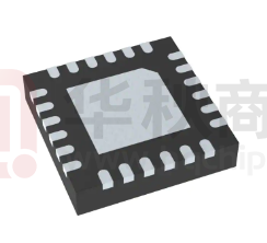
QFN-24 (4x4) Package
APPLICATIONS
D Motor Control
D Current Measurement
D Industrial Process Control
D Instrumentation
D Resolver
DESCRIPTION
The ADS1205 is a two-channel, high-performance,
delta-sigma (∆Σ) modulator with more than 98dB dynamic
range, operating from a single +5V supply. The differential
inputs are ideal for direct connection to transducers in an
industrial environment. With the appropriate digital filter
and modulator rate, the device can be used to achieve
16-bit analog-to-digital (A/D) conversion with no missing
codes. Effective resolution of 14 bits can be obtained with
a digital filter bandwidth of 40kHz at a modulator rate of
10MHz. The ADS1205 is designed for use in
high-resolution measurement applications including
current measurements, smart transmitters, industrial
process control, and resolvers. It is available in a QFN-24
(4x4) package.
AV DD
CH A+
CH A−
BV DD
OUT A
2nd−Order
∆Σ Modulator
Output
Interface
Circuit
CLKOUT
REFIN A
CH B+
CH B−
OUT B
2nd−Order
∆Σ Modulator
Divider
REFIN B
Clock
Select
Out
REFOUT
CLKIN
CLKSEL
EN
Reference
Voltage
2.5V
RC
Oscillator
20MHz
AGND
BGND
Please be aware that an important notice concerning availability, standard warranty, and use in critical applications of Texas Instruments
semiconductor products and disclaimers thereto appears at the end of this data sheet.
All trademarks are the property of their respective owners.
Copyright 2005−2007, Texas Instruments Incorporated
����!"�#�$ ���� ��%�������� �� &������ �� �% '�(��&����� ����) �����&��
&��%��� �� �'�&�%�&������ '�� �*� ����� �% ��+�� #���������� �������� �������,)
�����&���� '��&������ ���� ��� ��&�������, ��&���� ������� �% ��� '���������)
www.ti.com
������
�
www.ti.com
SBAS312B − JANUARY 2005 − REVISED AUGUST 2007
This integrated circuit can be damaged by ESD. Texas Instruments recommends that all integrated circuits be handled with appropriate
precautions. Failure to observe proper handling and installation procedures can cause damage.
ESD damage can range from subtle performance degradation to complete device failure. Precision integrated circuits may be more susceptible to
damage because very small parametric changes could cause the device not to meet its published specifications.
Package/Ordering Information
For the most current package and ordering information, see the Package Option Addendum at the end of this document,
or see the TI web site at www.ti.com.
ABSOLUTE MAXIMUM RATINGS
over operating free-air temperature range unless otherwise noted(1)
ADS1205
UNIT
Supply voltage, AGND to AVDD
−0.3 to 6
V
Supply voltage, BGND to BVDD
−0.3 to 6
V
AGND − 0.3 to AVDD + 0.3
AGND − 0.3 to AVDD + 0.3
V
Reference input voltage with respect to AGND
Digital input voltage with respect to BGND
BGND − 0.3 to BVDD + 0.3
V
±0.3
V
Analog input voltage with respect to AGND
Ground voltage difference, AGND to BGND
V
Voltage differences, BVDD to AGND
−0.3 to 6
V
Input current to any pin except supply
±10
mA
Power dissipation
See Dissipation Rating table
Operating virtual junction temperature range, TJ
−40 to +150
°C
Operating free-air temperature range, TA
−40 to +85
°C
Storage temperature range, TSTG
−65 to +150
°C
(1) Stresses beyond those listed under Absolute Maximum Ratings may cause permanent damage to the device. These are stress ratings only, and
functional operation of the device at these or any other conditions beyond those indicated under Recommended Operating Conditions is not
implied. Exposure to absolute-maximum-rated conditions for extended periods may affect device reliability.
DISSIPATION RATINGS
PACKAGE
TA ≤ 25°C
POWER RATING
DERATING FACTOR
ABOVE TA = 25°C(1)
21.929mW/°C
TA = 70°C
POWER RATING
TA = 85°C
POWER RATING
QFN-24 (4x4)
2193mW
1206mW
877.2mW
(1) This is the inverse of the traditional junction-to-ambient thermal resistance (Rq JA). Thermal resistances are not production tested and are for
informational purposes only.
RECOMMENDED OPERATING CONDITIONS
PARAMETER
Supply voltage, AGND to AVDD
Supply voltage, BGND to BVDD
MIN
NOM
MAX
UNIT
4.5
5
5.5
V
3.6
V
Low-Voltage Levels
2.7
5V Logic Levels
4.5
5
5.5
V
0.5
2.5
2.6
V
Reference input voltage
Operating common-mode signal
−IN
Analog inputs
+IN − (−IN)
2.5
External clock(1)
16
Operating junction temperature range, TJ
(1) With reduced accuracy, clock can go from 1MHz up to 33MHz; see Typical Characteristics.
−40
2
V
±0.8 × REFIN
20
V
24
MHz
105
°C
������
�
www.ti.com
SBAS312B − JANUARY 2005 − REVISED AUGUST 2007
ELECTRICAL CHARACTERISTICS
Over recommended operating free-air temperature range at −40°C to +85°C, AVDD = 5V, BVDD = 3V, CH x+ = 0.5V to 4.5V, CH x− = 2.5V,
REFIN = REFOUT = internal +2.5V, CLKIN = 20MHz, and 16-bit Sinc3 filter with decimation by 256, unless otherwise noted.
PARAMETER
Resolution
TEST CONDITIONS
MIN
ADS1205I
TYP(1)
MAX
16
UNITS
Bits
DC Accuracy
INL
Integral linearity error(2)
−1.4
±3
−0.002
±0.005
6
Integral linearity match
DNL
VOS
TCVOS
GERR
0.009
Differential nonlinearity(3)
Input offset error(4)
LSB
% FSR
±1
LSB
−1.2
±3
mV
Input offset error match
0.1
2
mV
Input offset error drift
Gain error(4)
1.1
8
µV/°C
−0.01
±0.5
% FSR
0.09
0.5
Referenced to VREF
Gain error match
TCGERR
PSRR
LSB
% FSR
Gain error drift
% FSR
1.3
ppm/°C
78
dB
Power-supply rejection ratio
4.75V < AVDD < 5.25V
Full-scale differential range
(CH x+) − (CH x−); CH x− = 2.5V
±2.5
V
Specified differential range
(CH x+) − (CH x−); CH x− = 2.5V
±2
V
Analog Input
FSR
Maximum operating input range(3)
0
Input capacitance
Common-mode
Input leakage current
CLK turned off
3
100
Differential input capacitance
Common-mode rejection ratio
BW
Bandwidth
V
pF
±1
Differential input resistance
CMRR
AVDD
nA
kΩ
2.5
pF
At DC
108
dB
VIN = ±1.25VPP at 40kHz
FS sine wave, −3dB
117
dB
50
MHz
Sampling Dynamics
Internal clock frequency
CLKSEL = 1
8
9.8
12
MHz
External clock frequency(5)
CLKSEL = 0
1
20
24
MHz
THD
Total harmonic distortion
−96.6
−88
dB
SFDR
Spurious-free dynamic range
VIN = ±2VPP at 5kHz
VIN = ±2VPP at 5kHz
SNR
Signal-to-noise ratio
SINAD
Signal-to-noise + distortion
VIN = ±2VPP at 5kHz
VIN = ±2VPP at 5kHz
Channel-to-channel isolation(3)
VIN = ±2VPP at 50kHz
CLKIN
AC Accuracy
ENOB
Effective number of bits
92
98
dB
86
88.9
dB
85
88.2
dB
14
100
dB
14.5
Bits
(1) All typical values are at TA = +25°C.
(2) Integral nonlinearity is defined as the maximum deviation of the line through the end points of the specified input range of the transfer curve
for CH x+ = −2V to +2V at 2.5V, expressed either as the number of LSBs or as a percent of measured input range (4V).
(3) Ensured by design.
(4) Maximum values, including temperature drift, are ensured over the full specified temperature range.
(5) With reduced accuracy, the clock frequency can go from 1MHz to 33MHz.
(6) Applicable for 5.0V nominal supply: BVDD (min) = 4.5V and BVDD (max) = 5.5V.
(7) Applicable for 3.0V nominal supply: BVDD (min) = 2.7V and BVDD (max) = 3.6V.
3
������
�
www.ti.com
SBAS312B − JANUARY 2005 − REVISED AUGUST 2007
ELECTRICAL CHARACTERISTICS (continued)
Over recommended operating free-air temperature range at −40°C to +85°C, AVDD = 5V, BVDD = 3V, CH x+ = 0.5V to 4.5V, CH x− = 2.5V,
REFIN = REFOUT = internal +2.5V, CLKIN = 20MHz, and 16-bit Sinc3 filter with decimation by 256, unless otherwise noted.
PARAMETER
Voltage Reference Output
VREFOUT
Reference voltage output
dVREFOUT/dT Output voltage temperature drift
Output voltage noise
TEST CONDITIONS
−40°C to +85°C
MIN
2.450
ADS1205I
TYP(1)
MAX
2.5
2.550
UNITS
V
±20
ppm/°C
f = 0.1Hz to 10Hz, CL = 10µF
10
µVrms
f =10Hz to 10kHz, CL = 10µF
12
µVrms
dB
PSRR
Power-supply rejection ratio
60
IOUT
ISC
Output current
10
µA
Short-circuit current
0.5
mA
100
µs
Turn-on settling time
to 0.1% at CL = 0
Voltage Reference Input
VIN
Reference voltage input
0.5
Reference input resistance
2.5
2.6
100
Reference input capacitance
5
pF
1
µA
BVDD+0.3
0.3×BVDD
V
±50
nA
Reference input current
Digital Inputs(6)
Logic family
VIH
VIL
High-level input voltage
IIN
CI
Input current
V
MΩ
CMOS with Schmitt Trigger
0.7×BVDD
−0.3
Low-level input voltage
VI = BVDD or GND
Input capacitance
5
V
pF
Digital Outputs(6)
Logic family
VOH
VOL
High-level output voltage
CO
CL
Output capacitance
Low-level output voltage
CMOS
BVDD = 4.5V, IOH = −100µA
BVDD = 4.5V, IOL = +100µA
4.44
V
0.5
5
Load capacitance
Data format
V
pF
30
pF
Bit Stream
(1) All typical values are at TA = +25°C.
(2) Integral nonlinearity is defined as the maximum deviation of the line through the end points of the specified input range of the transfer curve
for CH x+ = −2V to +2V at 2.5V, expressed either as the number of LSBs or as a percent of measured input range (4V).
(3) Ensured by design.
(4) Maximum values, including temperature drift, are ensured over the full specified temperature range.
(5) With reduced accuracy, the clock frequency can go from 1MHz to 33MHz.
(6) Applicable for 5.0V nominal supply: BVDD (min) = 4.5V and BVDD (max) = 5.5V.
(7) Applicable for 3.0V nominal supply: BVDD (min) = 2.7V and BVDD (max) = 3.6V.
4
������
�
www.ti.com
SBAS312B − JANUARY 2005 − REVISED AUGUST 2007
ELECTRICAL CHARACTERISTICS (continued)
Over recommended operating free-air temperature range at −40°C to +85°C, AVDD = 5V, BVDD = 3V, CH x+ = 0.5V to 4.5V, CH x− = 2.5V,
REFIN = REFOUT = internal +2.5V, CLKIN = 20MHz, and 16-bit Sinc3 filter with decimation by 256, unless otherwise noted.
PARAMETER
Digital Inputs(7)
MIN
TEST CONDITIONS
Logic family
ADS1205I
TYP(1)
MAX
UNITS
LVCMOS
VIH
VIL
High-level input voltage
Low-level input voltage
BVDD = 3.6V
BVDD = 2.7V
IIN
CI
Input current
VI = BVDD or GND
2
−0.3
Input capacitance
BVDD+0.3
0.8
V
±50
nA
5
V
pF
Digital Outputs(7)
Logic family
LVCMOS
VOH
VOL
High-level output voltage
CO
CL
Output capacitance
BVDD = 2.7V, IOH = −100µA
BVDD = 2.7V, IOL = +100µA
Low-level output voltage
BVDD−0.2
V
0.2
5
Load capacitance
Data format
V
pF
30
pF
Bit Stream
Power Supply
AVDD
BVDD
AIDD
BIDD
Analog supply voltage
Buffer I/O supply voltage
Analog operating supply current
Buffer I/O operating supply current
Power dissipation
4.5
5.5
V
Low-voltage levels
2.7
3.6
V
5V logic levels
4.5
5.5
V
CLKSEL = 1
11.8
16
mA
CLKSEL = 0
11.4
15.5
mA
2
mA
BVDD = 3V, CLKOUT = 10MHz
BVDD = 5V, CLKOUT = 10MHz
2
mA
CLKSEL = 0
57
77.5
mW
CLKSEL = 1
59
80
mW
(1) All typical values are at TA = +25°C.
(2) Integral nonlinearity is defined as the maximum deviation of the line through the end points of the specified input range of the transfer curve
for CH x+ = −2V to +2V at 2.5V, expressed either as the number of LSBs or as a percent of measured input range (4V).
(3) Ensured by design.
(4) Maximum values, including temperature drift, are ensured over the full specified temperature range.
(5) With reduced accuracy, the clock frequency can go from 1MHz to 33MHz.
(6) Applicable for 5.0V nominal supply: BVDD (min) = 4.5V and BVDD (max) = 5.5V.
(7) Applicable for 3.0V nominal supply: BVDD (min) = 2.7V and BVDD (max) = 3.6V.
EQUIVALENT INPUT CIRCUIT
BVDD
AVDD
R ON
650Ω
C(SAMPLE)
1pF
AIN
DIN
Diode Turn−On Voltage: 0.35V
AGND
Equivalent Analog Input Circuit
BGND
Equivalent Digital Input Circuit
5
������
�
www.ti.com
SBAS312B − JANUARY 2005 − REVISED AUGUST 2007
PIN ASSIGNMENT
19 NC(2)
20 CH A+
21 CH A−
22 CH B−
23 CH B+
24 NC(2)
RGE PACKAGE
QFN−24
(TOP VIEW)
REFIN B
1
18
REFIN A
AGND
2
17
AGND
AVDD
3
16
AVDD
AVDD
4
15
AVDD
AGND
5
14
REFOUT
CLKSEL
6
13
AGND
7
8
9
10
11
12
CLKIN
BVDD
BGND
CLKOUT
OUT B
OUT A
ADS1205(1)
(1) The thermal pad is internally connected to the substrate. This pad can be connected to the analog ground or left floating. Keep the thermal pad
separate from the digital ground, if possible.
(2) NC = No Connection.
Terminal Functions
TERMINAL
NAME
REFIN B
NO.
I/O
1
I
DESCRIPTION
Reference voltage input of channel B: pin for external reference voltage
AGND
2, 5, 13, 17
Analog ground
AVDD
3, 4, 15, 16
Analog power supply; nominal 5V
CLKSEL
6
I
Clock select between internal clock (CLKSEL = 1) or external clock (CLKSEL = 0)
CLKIN
7
I
External clock input
BVDD
8
Digital interface power supply; from 2.7V to 5.5V
BGND
9
Interface ground
CLKOUT
10
O
System clock output
OUT B
11
O
Bit stream from channel B modulator
OUT A
12
O
Bit stream from channel A modulator
REFOUT
14
O
Reference voltage output: output pin of the internal reference source; nominal 2.5V
REFIN A
18
I
Reference voltage input of channel A: pin for external reference voltage
NC
19, 24
No connection; this pin is left unconnected
CH A+
20
I
Analog input of channel A: noninverting input
CH A−
21
I
Analog input of channel A: inverting input
CH B−
22
I
Analog input of channel B: inverting input
CH B+
23
I
Analog input of channel B: noninverting input
6
������
�
www.ti.com
SBAS312B − JANUARY 2005 − REVISED AUGUST 2007
PARAMETER MEASUREMENT INFORMATION
tC1
CLKIN
t W1
tC2
tD1
tD2
CLKOUT
tD3
tW2
tD4
OUT x
Figure 1. ADS1205 Timing Diagram
TIMING REQUIREMENTS(1)
over recommended operating free-air temperature range at −40°C to +85°C, AVDD = 5V, and BVDD = 2.7 to 5V, unless otherwise noted.
MIN
41.6(2)
MAX
UNIT
1000
ns
CLKIN high time: (CLKSEL = 0)
10
83
tC1 − 10
125
ns
CLKOUT period using internal oscillator (CLKSEL = 1)
2 × tC1
(tC2/2) − 5
0
(tC2/2) + 5
10
ns
0
10
ns
(tC2/4) − 8
tW1 − 3
(tC2/4) + 8
tW1 + 7
ns
PARAMETER
tC1
tW1
CLKIN period: (CLKSEL = 0)
tC2
CLKOUT period using external clock (CLKSEL = 0)
tW2
tD1
CLKOUT high time
tD2
tD3
CLKOUT falling edge delay after CLKIN rising edge: (CLKOUT = 0)
CLKOUT rising edge delay after CLKIN rising edge: (CLKOUT = 0)
Data valid delay after rising edge of CLKOUT (CLKSEL = 1)
ns
ns
ns
tD4
Data valid delay after rising edge of CLKOUT (CLKSEL = 0)
ns
(1) All input signals are specified with tR = tF = 5ns (10% to 90% of BVDD) and timed from a voltage level of (VIL + VIH)/2. See Figure 1.
(2) With reduced accuracy, the minimum clock period can go down to 30ns.
7
������
�
www.ti.com
SBAS312B − JANUARY 2005 − REVISED AUGUST 2007
TYPICAL CHARACTERISTICS
AVDD = 5V, BVDD = 3V, CH x+ = 0.5V to 4.5V, CH x− = 2.5V, REFIN = REFOUT = internal +2.5V, CLKIN = 20MHz, and 16-bit Sinc3 filter with
decimation by 256, unless otherwise noted.
0.00259
1.7
0.00259
1.2
0.00183
1.2
0.00183
0.70
0.00107
0.70
0.00107
0.20
0.00031
+25_C
−0.00046
+85_C
−0.8
−1.3
−1.8
−2.5 −2.0 −1.5 −1.0 −0.5 0
0.5 1.0
Differential Input Voltage (V)
2.0
0.00031
−0.3
−0.00122
−0.8
−0.00198
−1.3
−40_C
1.5
0.20
+25_C
−0.00046
−0.00122
−0.00198
−1.8
−2.5 −2.0 −1.5 −1.0 −0.5 0
0.5 1.0
Differential Input Voltage (V)
−0.00275
2.5
Figure 2
−40_C
1.5
2.0
−0.00275
2.5
Figure 3
INTEGRAL LINEARITY MATCH OF CHANNELS
vs INPUT SIGNAL
INTEGRAL LINEARITY vs TEMPERATURE
0
0.00046
−0.2
−0.00031
0.2
0.00031
−0.4
−0.00061
0.1
0.00015
−0.6
−0.00092
−0.8
−0.00122
0.3
CLKIN = 20MHz
0
CLKIN = 32MHz
0
INL (%)
INL (LSB)
0.00061
0.4
INL (LSB)
+85_C
−0.1
−0.00015
−0.2
−0.00031
−1.2
−0.3
−0.00046
−1.4
−0.4
−2.5 −2.0 −1.5 −1.0 −0.5 0
0.5 1.0
Differential Input Voltage (V)
1.5
2.0
−0.00061
2.5
−1.0
0
−0.00153
CLKIN = 32MHz
−0.00183
−0.00214
CLKIN = 20MHz
−1.6
−40
−20
0
Figure 4
20
40
Temperature (_ C)
60
80
−0.00244
100
Figure 5
OFFSET vs TEMPERATURE
OFFSET MATCH vs TEMPERATURE
−1.0
0.15
0.14
0.13
Offset Match (mV)
Offset (mV)
−1.05
−1.10
−1.15
CLKIN = 32MHz
−1.20
CLKIN = 20MHz
0.09
0.08
0.06
CLKIN = 20MHz
−20
0
20
40
Temperature (_C)
Figure 6
8
0.11
0.10
0.07
−1.25
−1.30
−40
CLKIN = 32MHz
0.12
60
80
100
0.05
−40
−20
0
20
40
Temperature (_ C)
Figure 7
60
80
100
INL (%)
−0.3
INL (LSB)
1.7
INL (%)
INTEGRAL NONLINEARITY vs INPUT SIGNAL
(CLKIN = 32MHz)
INL (%)
INL (LSB)
INTEGRAL NONLINEARITY vs INPUT SIGNAL
(CLKIN = 20MHz)
������
�
www.ti.com
SBAS312B − JANUARY 2005 − REVISED AUGUST 2007
TYPICAL CHARACTERISTICS (continued)
AVDD = 5V, BVDD = 3V, CH x+ = 0.5V to 4.5V, CH x− = 2.5V, REFIN = REFOUT = internal +2.5V, CLKIN = 20MHz, and 16-bit Sinc3 filter with
decimation by 256, unless otherwise noted.
OFFSET vs POWER SUPPLY
REFERENCE VOLTAGE vs TEMPERATURE
−0.8
2.510
2.508
2.506
2.504
CLKIN = 32MHz
VREF (V)
Offset (mV)
−1.0
−1.2
CLKIN = 20MHz
2.502
2.500
2.498
2.496
−1.4
2.494
2.492
−1.6
4.50
2.490
4.75
5.00
5.25
5.50
−40
−20
0
Power Supply (V)
Figure 8
0.20
0.120
0.15
0.115
0.10
0.110
0.05
CLKIN = 20MHz
−0.05
CLKIN = 32MHz
−0.10
0.100
0.080
40
60
80
100
CLKIN = 32MHz
0.075
−40
100
−20
0
Temperature (_ C)
20
40
60
Temperature (_C)
Figure 10
Figure 11
SIGNAL−TO−NOISE RATIO
vs TEMPERATURE
89.0
80
CLKIN = 20MHz
0.090
−0.20
20
100
0.095
0.085
0
80
0.105
−0.15
−20
60
GAIN MATCH vs TEMPERATURE
0.125
Gain Match (%)
Gain (%)
GAIN vs TEMPERATURE
−0.25
−40
40
Figure 9
0.25
0
20
Temperature (_ C)
SIGNAL−TO−NOISE + DISTORTION
vs TEMPERATURE
89.2
CLKIN = 20MHz
88.9
89.0
88.8
88.8
88.6
SINAD (dB)
SNR (dB)
88.7
CLKIN = 32MHz
88.5
88.4
88.3
88.4
CLKIN = 20MHz
88.2
88.0
88.2
88.1
88.6
CLKIN = 32MHz
4VPP
5kHz
4VPP
5kHz
87.8
88.0
87.6
−40
−20
0
20
40
Temperature (_C)
Figure 12
60
80
100
−40
−20
0
20
40
Temperature (_C)
60
80
100
Figure 13
9
������
�
www.ti.com
SBAS312B − JANUARY 2005 − REVISED AUGUST 2007
TYPICAL CHARACTERISTICS (continued)
AVDD = 5V, BVDD = 3V, CH x+ = 0.5V to 4.5V, CH x− = 2.5V, REFIN = REFOUT = internal +2.5V, CLKIN = 20MHz, and 16-bit Sinc3 filter with
decimation by 256, unless otherwise noted.
SPURIOUS FREE DYNAMIC RANGE AND
TOTAL HARMONIC DISTORTION vs TEMPERATURE
(CLKIN = 20MHz)
SPURIOUS FREE DYNAMIC RANGE AND
TOTAL HARMONIC DISTORTION vs TEMPERATURE
(CLKIN = 32MHz)
101
−101
101
99
−99
99
SFDR
−97
97
THD
95
−95
−93
−91
91
89
−89
89
−87
87
−20
0
20
40
Temperature (_C)
60
80
−97
−95
−91
−85
100
−99
THD
93
91
85
−40
−101
95
−93
4VPP
5kHz
−103
SFDR
97
93
87
−105
THD (dB)
103
SFDR (dB)
105
−103
THD (dB)
−105
103
SFDR (dB)
105
−89
4VPP
5kHz
85
−40
−20
Figure 14
−87
0
20
40
Temperature (_C)
60
80
−85
100
Figure 15
SIGNAL−TO−NOISE AND DISTORTION AND
SIGNAL−TO−NOISE RATIO vs INPUT FREQUENCY
(CLKIN = 20MHz)
SIGNAL−TO−NOISE AND DISTORTION AND
SIGNAL−TO−NOISE RATIO vs INPUT FREQUENCY
(CLKIN = 32MHz)
100
100
98
SINAD and SNR (dB)
94
92
SNR
90
88
SINAD
86
84
82
90
SNR
SINAD
85
OSR = 256
Sinc3 Filter
80
100
OSR = 256
Sinc3 Filter
1k
Input Frequency (kHz)
80
100
100k
100k
Figure 17
SPURIOUS FREE DYNAMIC RANGE AND
TOTAL HARMONIC DISTORTION vs INPUT FREQUENCY
(CLKIN = 20MHz)
SPURIOUS FREE DYNAMIC RANGE AND
TOTAL HARMONIC DISTORTION vs INPUT FREQUENCY
(CLKIN = 32MHz)
−120
120
−120
110
−110
110
−110
SFDR
−100
100
SFDR (dB)
120
SFDR
100
−90
OSR = 256
Sinc3 Filter
80
100
1k
10k
Input Frequency (Hz)
Figure 18
−80
100k
−100
THD
THD
90
10
1k
10k
Input Frequency (kHz)
Figure 16
THD (dB)
SFDR (dB)
95
−90
90
OSR = 256
Sinc3 Filter
80
100
1k
10k
Input Frequency (Hz)
Figure 19
−80
100k
THD (dB)
SINAD and SNR (dB)
96
������
�
www.ti.com
SBAS312B − JANUARY 2005 − REVISED AUGUST 2007
TYPICAL CHARACTERISTICS (continued)
AVDD = 5V, BVDD = 3V, CH x+ = 0.5V to 4.5V, CH x− = 2.5V, REFIN = REFOUT = internal +2.5V, CLKIN = 20MHz, and 16-bit Sinc3 filter with
decimation by 256, unless otherwise noted.
FREQUENCY SPECTRUM
(4096 point FFT fIN = 5kHz, 4VPP )
0
0
−20
−20
−40
−40
Magnitude (dB)
Magnitude (dB)
FREQUENCY SPECTRUM
(4096 point FFT fIN = 1kHz, 4VPP )
−60
−80
−100
−60
−80
−100
−120
−120
−140
−140
−160
−160
0
2
4
6
8
10
12
14
16
0
18 19
2
4
6
Frequency (kHz)
Figure 20
Sinc2 Filter
98
16
86
15
14
Current (mA)
74
SNR (dB)
12
14
16
18 19
CLKSEL = 0, CLKIN = 32MHz
13
10
62
8
50
6
38
4
26
9
14
8
12
11
CLKSEL = 0, CLKIN = 20MHz
10
CLKSEL = 1
2
10
100
1k
−40
Decimation Ratio (OSR)
0
20
40
60
80
100
Figure 23
COMMON−MODE REJECTION RATIO
vs FREQUENCY
POWER−SUPPLY REJECTION RATIO
vs FREQUENCY
100
120
90
PSRR (dB)
130
110
100
90
100
−20
Temperature (_C)
Figure 22
CMRR (dB)
ENOB (Bits)
12
POWER−SUPPLY CURRENT
vs TEMPERATURE
Sinc3 Filter
14
10
Figure 21
EFFECTIVE NUMBER OF BITS
vs DECIMATION RATIO
16
8
Frequency (kHz)
80
70
1k
10k
100k
Input Frequency (kHz)
Figure 24
1M
60
100
1k
Frequency of Power Supply (kHz)
10k
Figure 25
11
������
�
www.ti.com
SBAS312B − JANUARY 2005 − REVISED AUGUST 2007
TYPICAL CHARACTERISTICS (continued)
AVDD = 5V, BVDD = 3V, CH x+ = 0.5V to 4.5V, CH x− = 2.5V, REFIN = REFOUT = internal +2.5V, CLKIN = 20MHz, and 16-bit Sinc3 filter with
decimation by 256, unless otherwise noted.
10.8
10.1
10.6
10.0
10.4
9.9
10.2
10.0
9.8
9.6
9.8
9.7
9.6
9.5
9.4
9.4
9.2
9.3
9.0
−40
−20
9.2
0
20
40
Temperature (_ C)
Figure 26
12
CLOCK FREQUENCY vs POWER SUPPLY
10.2
CLKOUT (MHz)
CLKOUT (MHz)
CLOCK FREQUENCY vs TEMPERATURE
11.0
60
80
100
4.5
4.75
5
Power Supply (V)
Figure 27
5.25
5.5
������
�
www.ti.com
SBAS312B − JANUARY 2005 − REVISED AUGUST 2007
GENERAL DESCRIPTION
The ADS1205 is a two-channel, 2nd-order, CMOS device
with two delta-sigma modulators, designed for medium- to
high-resolution A/D signal conversions from DC to 39kHz
(filter response −3dB) if an oversampling ratio (OSR) of 64
is chosen. The output of the converter (OUTX) provides a
stream of digital ones and zeros. The time average of this
serial output is proportional to the analog input voltage.
The modulator shifts the quantization noise to high
frequencies. A low-pass digital filter should be used at the
output of the delta-sigma modulator. The filter serves two
functions. First, it filters out high-frequency noise. Second,
the filter converts the 1-bit data stream at a high sampling
rate into a higher-bit data word at a lower rate (decimation).
An application-specific integrated circuit (ASIC) or
field-programmable gate array (FPGA) could be used to
implement the digital filter. Figure 28 and Figure 29 show
typical application circuits with the ADS1205 connected to
an FPGA or ASIC.
The overall performance (that is, speed and accuracy)
depends on the selection of an appropriate OSR and filter
type. A higher OSR produces greater output accuracy
while operating at a lower refresh rate. Alternatively, a
lower OSR produces lower output accuracy, but operates
at a higher refresh rate. This system allows flexibility with
the digital filter design and is capable of A/D conversion
results that have a dynamic range exceeding 98dB with an
OSR = 256.
2 kΩ
AVDD
+5V
BVDD
5kΩ
±5V
27Ω
0.1µF
CH A+
OPA 2350
0.1nF
5kΩ
CH A−
2nd−Order
∆Σ Modulator
2kΩ
OUT A
OUT B
Output
Interface
Circuit
FPGA
or
ASIC
REFIN A
CLKOUT
2kΩ
CH B+
CH B−
+5V
2nd−Order
∆Σ Modulator
BVDD
0.1µF
BGND
5kΩ
±5V
27Ω
0.1µF
REFIN B
OPA 2350
Divider
0.1nF
5kΩ
+3V
2kΩ
+3V
Clock
Select
CLKIN
CLKSEL
+5V
AVDD
Out
REFOUT
Reference
Voltage
2.5V
+5V
EN
RC
Oscillator
20MHz
AVDD
AVDD
AVDD
AGND AGND AGND AGND
+5V
+5V
0.1µF
0.1µF
0.1µF
0.1µF
0.1µF
+5V
OP A 336
0.1µF
Figure 28. Single-Ended Connection Diagram for the ADS1205 Delta-Sigma Modulator
13
������
�
www.ti.com
SBAS312B − JANUARY 2005 − REVISED AUGUST 2007
AVDD
+5V
BVD D
27Ω
R1
CH A+
OP A 435 4
IN+
CH A−
0.1nF
2nd−Order
∆Σ Modulator
R2
OUT A
OUT B
Output
Interface
Circuit
FPGA
or
ASIC
REFIN A
CLKOUT
+5V
CH B+
27Ω
R1
OP A 435 4
CH B−
2nd−Order
∆Σ Modulator
+3V
BVD D
0.1µF
BGND
IN−
REFIN B
R2
Divider
+5V
+3V
27Ω
R1
Clock
Select
OP A 435 4
IN+
CLKIN
CLKSEL
0.1nF
+5V
R2
AVD D
Out
+5V
27Ω
R1
OP A 435 4
IN−
REFOUT
R2
Reference
Voltage
2.5V
+5V
EN
RC
Oscillator
20MHz
AVD D
AVD D
AVD D
AGND AGND AGND AGND
+5V
+5V
0.1µF
0.1µF
0.1µF
0.1µF
+5V
OP A33 6
0.1µF
Figure 29. Differential Connection Diagram for the ADS1205 Delta-Sigma Modulator
14
0.1µF
������
�
www.ti.com
SBAS312B − JANUARY 2005 − REVISED AUGUST 2007
THEORY OF OPERATION
The differential analog input of the ADS1205 is
implemented with a switched-capacitor circuit. This circuit
implements a 2nd-order modulator stage, which digitizes
the analog input signal into a 1-bit output stream. The clock
source can be internal as well as external. Different
frequencies for this clock allow for a variety of solutions
and signal bandwidths. Every analog input signal is
continuously sampled by the modulator and compared to
a reference voltage that is applied to the REFINx pin. A
digital stream, which accurately represents the analog
input voltage over time, appears at the output of the
corresponding converter.
ANALOG INPUT STAGE
Analog Input
The topology of the analog inputs of ADS1205 is based on
a fully differential switched-capacitor architecture. This
input stage provides the mechanism to achieve low
system noise, high common-mode rejection (108dB), and
excellent power-supply rejection.
The input impedance of the analog input is dependent on
the modulator clock frequency (fCLK), which is also the
sampling frequency of the modulator. Figure 30 shows the
basic input structure of one channel of the ADS1205. The
relationship between the input impedance of the ADS1205
and the modulator clock frequency is:
Z IN +
100kW
f MODń10MHz
(1)
The input impedance becomes a consideration in designs
where the source impedance of the input signal is high.
This high impedance may cause degradation in gain,
linearity, and THD. The importance of this effect depends
on the desired system performance. There are two
restrictions on the analog input signals, CH x+ and CH x−.
If the input voltage exceeds the range (GND – 0.3V) to
(VDD + 0.3V), the input current must be limited to 10mA
because the input protection diodes on the front end of the
converter will begin to turn on. In addition, the linearity and
the noise performance of the device are ensured only
when the differential analog voltage resides within ±2V
(with VREF as a midpoint); however, the FSR input voltage
is ±2.5V.
Modulator
The ADS1205 can be operated in two modes. When
CKLSEL = 1, the two modulators operate using the internal
clock, which is fixed at 20MHz. When CKLSEL = 0, the
modulators operate using an external clock. In both modes,
the clock is divided by two internally and functions as the
modulator clock. The frequency of the external clock can vary
from 1MHz to 33MHz to adjust for the clock requirements of
the application.
The modulator topology is fundamentally a 2nd-order,
switched-capacitor, delta-sigma modulator, such as the one
conceptualized in Figure 31. The analog input voltage and
the output of the 1-bit digital-to-analog converter (DAC) are
differentiated, providing analog voltages at X2 and X3. The
voltages at X2 and X3 are presented to their individual
integrators. The output of these integrators progresses in a
negative or positive direction. When the value of the signal
at X4 equals the comparator reference voltage, the output of
the comparator switches from negative to positive, or positive
to negative, depending on its original state. When the output
value of the comparator switches from high to low or vice
versa, the 1-bit DAC responds on the next clock pulse by
changing its analog output voltage at X6, causing the
integrators to progress in the opposite direction. The
feedback of the modulator to the front end of the integrators
forces the value of the integrator output to track the average
of the input.
650Ω
AIN+
1.2pF
0.4pF
VCM
Switching Frequency = CLK
0.4pF
AIN−
High
Impedance
> 1GΩ
650Ω
1.2pF
High
Impedance
> 1GΩ
Figure 30. Input Impedance of the ADS1205
15
������
�
www.ti.com
SBAS312B − JANUARY 2005 − REVISED AUGUST 2007
fCLK
X2
X(t)
Integrator 1
X3
Integrator 2
X4
DATA
fS
VREF
Comparator
X6
D/A Converter
Figure 31. Block Diagram of the 2nd-Order Modulator
DIGITAL OUTPUT
A differential input signal of 0V will ideally produce a
stream of ones and zeros that are high 50% of the time and
low 50% of the time. A differential input of +2V produces
a stream of ones and zeros that are high 80% of the time.
A differential input of –2V produces a stream of ones and
zeros that are high 20% of the time. The input voltage
versus the output modulator signal is shown in Figure 32.
DIGITAL INTERFACE
INTRODUCTION
The analog signal connected to the input of the
delta-sigma modulator is converted using the clock signal
applied to the modulator. The result of the conversion, or
modulation, is generated and sent to the OUTx pin from the
delta-sigma modulator. In most applications where a direct
connection is realized between the delta-sigma modulator
and an ASIC or FPGA (each with an implemented filter),
the two standard signals per modulator (CLKOUT and
OUTx) are provided from the modulator. The output clock
signal is equal for both modulators. If CLKSEL = 1, CLKIN
must always be set either high or low.
MODES OF OPERATION
The system clock of the ADS1205 is 20MHz by default.
The system clock can be provided either from the internal
20MHz RC oscillator or from an external clock source. For
this purpose, the CLKIN pin is provided; it is controlled by
the mode setting, CLKSEL.
The system clock is divided by two for the modulator clock.
Therefore, the default clock frequency of the modulator is
10MHz. With a possible external clock range of 1MHz to
33MHz, the modulator operates between 500kHz and
16.5MHz.
Modulator Output
+FS (Analog Input)
−FS (Analog Input)
Analog Input
Figure 32. Analog Input vs Modulator Output of the ADS1205
16
������
�
www.ti.com
SBAS312B − JANUARY 2005 − REVISED AUGUST 2007
FILTER USAGE
0
A very simple filter, built with minimal effort and
hardware, is the Sinc3 filter:
ǒ
Ǔ
−OSR
H(z) + 1 * z −1
1*z
OSR = 32
f DATA = 10MHz/32 = 312.5kHz
−3dB: 81.9kHz
−10
−20
Gain (dB)
The modulator generates only a bitstream, which does
not output a digital word like an A/D converter. In order
to output a digital word equivalent to the analog input
voltage, the bitstream must be processed by a digital
filter.
−30
−40
−50
−60
3
−70
(2)
This filter provides the best output performance at the
lowest hardware size (for example, a count of digital
gates). For oversampling ratios in the range of 16 to
256, this is a good choice. All the characterizations in
the data sheet are also done using a Sinc3 filter with an
oversampling ratio of OSR = 256 and an output word
length of 16 bits.
−80
0
This performance can be improved, for example, by a
cascaded filter structure. The first decimation stage can
be a Sinc3 filter with a low OSR and the second stage
a high-order filter.
For more information, see application note SBAA094,
Combining the ADS1202 with an FPGA Digital Filter for
Current Measurement in Motor Control Applications,
available for download at www.ti.com.
400
600
800 1000
Frequency (kHz)
1200
1400
1600
Figure 33. Frequency Response of Sinc3 Filter
30k
In a Sinc3 filter response (shown in Figure 33 and
OSR = 32
FSR = 32768
ENOB = 9.9 Bits
Settling Time =
3 × 1/f DATA = 9.6µs
25k
Output Code
Figure 34), the location of the first notch occurs at the
frequency of output data rate fDATA = fCLK/OSR. The
–3dB point is located at half the Nyquist frequency or
fDATA/4. For some applications, it may be necessary to
use another filter type for better frequency response.
200
20k
15k
10k
5k
0
0
5
10
15
20
25
30
Number of Output Clocks
35
40
Figure 34. Pulse Response of Sinc3 Filter
(fMOD = 10MHz)
17
������
�
www.ti.com
SBAS312B − JANUARY 2005 − REVISED AUGUST 2007
The effective number of bits (ENOB) can be used to
compare the performance of ADCs and delta-sigma
modulators. Figure 35 shows the ENOB of the
ADS1205 with different filter types. In this data sheet,
the ENOB is calculated from the SNR:
SNR = 1.76dB + 6.02dB × ENOB
(3)
filter types other than Sinc3 might be a better choice. A
simple example is a Sinc2 filter. The Sincfast is a
modified Sinc2 filter:
ǒ
Ǔ
2
−OSR
H(z) + 1 * z −1 ǒ1 ) z −2
1*z
Ǔ
OSR
(4)
Figure 36 compares the settling time of different filter
types operating with a 10MHz modulator clock.
16
Sinc3
14
10
10
8
8
7
6
Sinc
Sincfast
Sinc3
9
Sinc2
ENOB (Bits)
ENOB (Bits)
12
4
2
Sincfast
Sinc2
6
5
Sinc
4
3
0
2
1
10
100
1000
OSR
1
0
Figure 35. Measured ENOB vs OSR
In motor control applications, a very fast response time
for overcurrent detection is required. There is a
constraint between 1µs and 5µs with 3 bits to 7 bits
resolution. The time for full settling is dependent on the
filter order. Therefore, the full settling of the Sinc3 filter
needs three data clocks and the Sinc2 filter needs two
data clocks. The data clock is equal to the modulator
clock divided by the OSR. For overcurrent protection,
18
0
2
4
6
8
10
Settling Time (µs)
Figure 36. Measured ENOB vs Settling Time
For more information, see application note SBAA094,
Combining the ADS1202 with an FPGA Digital Filter for
Current Measurement in Motor Control Applications,
available for download at www.ti.com.
������
�
www.ti.com
SBAS312B − JANUARY 2005 − REVISED AUGUST 2007
LAYOUT CONSIDERATIONS
POWER SUPPLIES
An applied external digital filter rejects high-frequency
noise. PSRR and CMRR improve at higher frequencies
because the digital filter suppresses high-frequency noise.
However, the suppression of the filter is not infinite, so
high-frequency noise still influences the conversion result.
For multiple converters, connect the two ground planes as
close as possible to one central location for all of the
converters. In some cases, experimentation may be
required to find the best point to connect the two planes
together.
DECOUPLING
Inputs to the ADS1205, such as CH x+, CH x−, and CLKIN,
should not be present before the power supply is on.
Violating this condition could cause latch-up. If these
signals are present before the supply is on, series resistors
should be used to limit the input current to a maximum of
10mA. Experimentation may be the best way to determine
the appropriate connection between the ADS1205 and
different power supplies.
Good decoupling practices must be used for the ADS1205
and for all components in the design. All decoupling
capacitors, specifically the 0.1µF ceramic capacitors,
must be placed as close as possible to the pin being
decoupled. A 1µF and 10µF capacitor, in parallel with the
0.1µF ceramic capacitor, can be used to decouple AVDD
to AGND as well as BVDD to BGND. At least one 0.1µF
ceramic capacitor must be used to decouple every AVDD
to AGND and BVDD to BGND, as well as for the digital
supply on each digital component.
GROUNDING
The digital supply sets the I/O voltage for the interface and
can be set within a range of 2.7V to 5.5V.
Analog and digital sections of the design must be carefully
and cleanly partitioned. Each section should have its own
ground plane with no overlap between them. Do not join
the ground planes; instead, connect the two with a
moderate signal trace underneath the converter. However,
for different applications with DSPs and switching power
supplies, this process might be different.
In cases where both the analog and digital I/O supplies
share the same supply source, an RC filter of 10Ω and
0.1µF can be used to help reduce the noise in the analog
supply.
19
�Revision History
DATE
REV
PAGE
8/06
B
6
SECTION
Pin Assignment
DESCRIPTION
Added Note 1 to QFN package.
NOTE: Page numbers for previous revisions may differ from page numbers in the current version.
�PACKAGE OPTION ADDENDUM
www.ti.com
10-Aug-2007
PACKAGING INFORMATION
Orderable Device
Status (1)
Package
Type
Package
Drawing
Pins Package Eco Plan (2)
Qty
ADS1205IRGER
ACTIVE
QFN
RGE
24
3000 Green (RoHS &
no Sb/Br)
CU NIPDAU
Level-2-260C-1 YEAR
ADS1205IRGERG4
ACTIVE
QFN
RGE
24
3000 Green (RoHS &
no Sb/Br)
CU NIPDAU
Level-2-260C-1 YEAR
ADS1205IRGET
ACTIVE
QFN
RGE
24
250
Green (RoHS &
no Sb/Br)
CU NIPDAU
Level-2-260C-1 YEAR
ADS1205IRGETG4
ACTIVE
QFN
RGE
24
250
Green (RoHS &
no Sb/Br)
CU NIPDAU
Level-2-260C-1 YEAR
Lead/Ball Finish
MSL Peak Temp (3)
(1)
The marketing status values are defined as follows:
ACTIVE: Product device recommended for new designs.
LIFEBUY: TI has announced that the device will be discontinued, and a lifetime-buy period is in effect.
NRND: Not recommended for new designs. Device is in production to support existing customers, but TI does not recommend using this part in
a new design.
PREVIEW: Device has been announced but is not in production. Samples may or may not be available.
OBSOLETE: TI has discontinued the production of the device.
(2)
Eco Plan - The planned eco-friendly classification: Pb-Free (RoHS), Pb-Free (RoHS Exempt), or Green (RoHS & no Sb/Br) - please check
http://www.ti.com/productcontent for the latest availability information and additional product content details.
TBD: The Pb-Free/Green conversion plan has not been defined.
Pb-Free (RoHS): TI's terms "Lead-Free" or "Pb-Free" mean semiconductor products that are compatible with the current RoHS requirements
for all 6 substances, including the requirement that lead not exceed 0.1% by weight in homogeneous materials. Where designed to be soldered
at high temperatures, TI Pb-Free products are suitable for use in specified lead-free processes.
Pb-Free (RoHS Exempt): This component has a RoHS exemption for either 1) lead-based flip-chip solder bumps used between the die and
package, or 2) lead-based die adhesive used between the die and leadframe. The component is otherwise considered Pb-Free (RoHS
compatible) as defined above.
Green (RoHS & no Sb/Br): TI defines "Green" to mean Pb-Free (RoHS compatible), and free of Bromine (Br) and Antimony (Sb) based flame
retardants (Br or Sb do not exceed 0.1% by weight in homogeneous material)
(3)
MSL, Peak Temp. -- The Moisture Sensitivity Level rating according to the JEDEC industry standard classifications, and peak solder
temperature.
Important Information and Disclaimer:The information provided on this page represents TI's knowledge and belief as of the date that it is
provided. TI bases its knowledge and belief on information provided by third parties, and makes no representation or warranty as to the
accuracy of such information. Efforts are underway to better integrate information from third parties. TI has taken and continues to take
reasonable steps to provide representative and accurate information but may not have conducted destructive testing or chemical analysis on
incoming materials and chemicals. TI and TI suppliers consider certain information to be proprietary, and thus CAS numbers and other limited
information may not be available for release.
In no event shall TI's liability arising out of such information exceed the total purchase price of the TI part(s) at issue in this document sold by TI
to Customer on an annual basis.
Addendum-Page 1
�PACKAGE MATERIALS INFORMATION
www.ti.com
10-Aug-2007
TAPE AND REEL INFORMATION
Pack Materials-Page 1
�PACKAGE MATERIALS INFORMATION
www.ti.com
Device
10-Aug-2007
Package Pins
Site
Reel
Diameter
(mm)
Reel
Width
(mm)
A0 (mm)
B0 (mm)
K0 (mm)
P1
(mm)
W
Pin1
(mm) Quadrant
ADS1205IRGER
RGE
24
TAI
330
12
4.3
4.3
1.5
8
12
Q2
ADS1205IRGET
RGE
24
TAI
330
12
4.3
4.3
1.5
8
12
Q2
TAPE AND REEL BOX INFORMATION
Device
Package
Pins
Site
Length (mm)
Width (mm)
Height (mm)
ADS1205IRGER
RGE
24
TAI
407.0
336.6
97.0
ADS1205IRGET
RGE
24
TAI
407.0
336.6
97.0
Pack Materials-Page 2
��This package incorporates an exposed thermal pad that is designed to be attached directly to an external heatsink. The
thermal pad must be soldered directly to the printed circuit board (PCB). After soldering, the PCB can be used as a
heatsink. In addition, through the use of thermal vias, the thermal pad can be attached directly to the appropriate copper
plane shown in the electrical schematic for the device, or alternatively, can be attached to a special heatsink structure
designed into the PCB. This design optimizes the heat transfer from the integrated circuit (IC).
��PACKAGE MATERIALS INFORMATION
www.ti.com
1-Sep-2021
TAPE AND REEL INFORMATION
*All dimensions are nominal
Device
ADS1205IRGER
Package Package Pins
Type Drawing
VQFN
RGE
24
SPQ
Reel
Reel
A0
Diameter Width (mm)
(mm) W1 (mm)
3000
330.0
12.4
Pack Materials-Page 1
4.3
B0
(mm)
K0
(mm)
P1
(mm)
4.3
1.5
8.0
W
Pin1
(mm) Quadrant
12.0
Q2
�PACKAGE MATERIALS INFORMATION
www.ti.com
1-Sep-2021
*All dimensions are nominal
Device
Package Type
Package Drawing
Pins
SPQ
Length (mm)
Width (mm)
Height (mm)
ADS1205IRGER
VQFN
RGE
24
3000
350.0
350.0
43.0
Pack Materials-Page 2
�IMPORTANT NOTICE AND DISCLAIMER
TI PROVIDES TECHNICAL AND RELIABILITY DATA (INCLUDING DATASHEETS), DESIGN RESOURCES (INCLUDING REFERENCE
DESIGNS), APPLICATION OR OTHER DESIGN ADVICE, WEB TOOLS, SAFETY INFORMATION, AND OTHER RESOURCES “AS IS”
AND WITH ALL FAULTS, AND DISCLAIMS ALL WARRANTIES, EXPRESS AND IMPLIED, INCLUDING WITHOUT LIMITATION ANY
IMPLIED WARRANTIES OF MERCHANTABILITY, FITNESS FOR A PARTICULAR PURPOSE OR NON-INFRINGEMENT OF THIRD
PARTY INTELLECTUAL PROPERTY RIGHTS.
These resources are intended for skilled developers designing with TI products. You are solely responsible for (1) selecting the appropriate
TI products for your application, (2) designing, validating and testing your application, and (3) ensuring your application meets applicable
standards, and any other safety, security, or other requirements. These resources are subject to change without notice. TI grants you
permission to use these resources only for development of an application that uses the TI products described in the resource. Other
reproduction and display of these resources is prohibited. No license is granted to any other TI intellectual property right or to any third party
intellectual property right. TI disclaims responsibility for, and you will fully indemnify TI and its representatives against, any claims, damages,
costs, losses, and liabilities arising out of your use of these resources.
TI’s products are provided subject to TI’s Terms of Sale (https:www.ti.com/legal/termsofsale.html) or other applicable terms available either
on ti.com or provided in conjunction with such TI products. TI’s provision of these resources does not expand or otherwise alter TI’s
applicable warranties or warranty disclaimers for TI products.IMPORTANT NOTICE
Mailing Address: Texas Instruments, Post Office Box 655303, Dallas, Texas 75265
Copyright © 2021, Texas Instruments Incorporated
�