User's Guide
SBAU090E – November 2003 – Revised November 2018
ADS1256EVM and ADS1256EVM-PDK
This user's guide describes the characteristics, operation, and use of the ADS1256EVM, both by itself and
as part of the ADS1256EVM-PDK. This EVM is an evaluation fixture for the ADS1256 24-bit delta-sigma
(ΔΣ) analog-to-digital converter (ADC). It also serves as an evaluation platform for the ADS1255, which is
a proper subset of the ADS1256. It allows evaluation of all aspects of the ADS1256 device. A complete
circuit description, schematic diagram, and bill of materials are included.
The following related documents are available through the Texas Instruments web site at www.ti.com.
Device
Literature Number
ADS1256
SBAS288
REF5025
SBOS410
OPA350
SBOS099
SBAU090E – November 2003 – Revised November 2018
Submit Documentation Feedback
ADS1256EVM and ADS1256EVM-PDK
Copyright © 2003–2018, Texas Instruments Incorporated
1
�www.ti.com
1
2
3
4
5
6
7
8
9
10
Contents
EVM Overview ............................................................................................................... 3
Analog Interface.............................................................................................................. 6
Digital Interface .............................................................................................................. 7
Power Supplies .............................................................................................................. 8
Voltage Reference ......................................................................................................... 10
Clock Source ................................................................................................................ 11
EVM Operation ............................................................................................................. 12
ADS1256EVM-PDK Kit Operation ....................................................................................... 15
Evaluating Performance with the ADCPro Software ................................................................... 30
Schematics and Layout .................................................................................................... 38
List of Figures
1
ADS1256EVM ................................................................................................................ 5
2
GPIO Pins
3
Jumper Block ................................................................................................................. 9
4
Switch S3 .................................................................................................................... 10
5
Switch S4 .................................................................................................................... 11
6
Switches S1 and S2
7
8
9
10
11
12
13
14
15
16
17
18
19
20
21
22
23
24
25
26
27
28
29
30
31
32
33
34
35
36
2
....................................................................................................................
.......................................................................................................
ADS1256EVM Default Jumper and Switch Locations .................................................................
ADS1256EVM-PDK Setup Wizard .......................................................................................
ADS1256EVM-PDK License Agreement ................................................................................
ADS1256EVM-PDK Installation in Progress ............................................................................
ADS1256EVM-PDK Installation Complete ..............................................................................
MMB0 Initial Configuration ................................................................................................
Connecting the ADS1256EVM to the MMB0 ...........................................................................
MMB0 Powered From AC Adapter.......................................................................................
MMB0 Configured for Lab Power Supply ...............................................................................
NI-VISA Driver Installation Wizard, Screen 1 ...........................................................................
NI-VISA Driver Installation Wizard, Screen 2 ...........................................................................
NI-VISA Driver Installation Wizard, Screen 3 ...........................................................................
NI-VISA Driver Installation Wizard, Screen 4 ...........................................................................
NI-VISA Driver Verification Using Device Manager....................................................................
ADCPro Software Start-up Display Window ............................................................................
ADS1256EVM-PDK Plug-In Display Window ..........................................................................
Install New Driver Wizard Screen 1......................................................................................
Install New Driver Wizard Screen 2......................................................................................
Install New Driver Wizard Screen 3......................................................................................
Install New Driver Wizard Screen 4......................................................................................
Install New Driver Wizard Screen 5......................................................................................
USBStyx Driver Verification Using Device Manager...................................................................
ADS1256EVM-PDK Plug-In Averages, PGA Gain, and Effective Data Rate Controls ...........................
MUX Tab ....................................................................................................................
Clocks Tab ..................................................................................................................
GPIO Tab ...................................................................................................................
Power & Ref Tab ...........................................................................................................
Cal Tab ......................................................................................................................
EVM Software About Tab .................................................................................................
Software Progress Indicator ..............................................................................................
ADS1256EVM and ADS1256EVM-PDK
8
12
14
16
16
17
17
18
19
20
21
22
23
23
24
25
25
26
27
27
28
28
29
29
30
31
32
33
34
35
36
37
SBAU090E – November 2003 – Revised November 2018
Submit Documentation Feedback
Copyright © 2003–2018, Texas Instruments Incorporated
�EVM Overview
www.ti.com
37
ADS1256EVM PCB: Top-Side Image ................................................................................... 39
38
ADS1256EVM PCB: Layer 1 ............................................................................................. 39
39
ADS1256EVM PCB: Layer 2 ............................................................................................. 39
40
ADS1256EVM PCB: Bottom-Side Image ............................................................................... 39
41
Schematic ................................................................................................................... 40
List of Tables
1
J1: Analog Interface Pinout ................................................................................................. 6
2
J2: Serial Interface Pins..................................................................................................... 7
3
J5: GPIO Header Pins ...................................................................................................... 8
4
J5 Configuration: Power-Supply Input
5
J4, J9, and J10 Configuration: Power Options ......................................................................... 10
6
Reference Input Select Switch
7
8
9
10
11
12
....................................................................................
...........................................................................................
System Clock Select Switch ..............................................................................................
AIN0-1 Input Select Switch (S1)..........................................................................................
AIN2-3 Input Select Switch (S2)..........................................................................................
Default Jumper Positions..................................................................................................
Default Switch Positions ...................................................................................................
ADS1256EVM Bill of Materials ..........................................................................................
8
11
11
12
13
14
15
38
Trademarks
ADCPro is a trademark of Texas Instruments.
Microsoft, Windows are registered trademarks of Microsoft Corporation.
I2C is a trademark of NXP Semiconductors.
NI-VISA is a trademark of National Instruments.
All other trademarks are the property of their respective owners.
1
EVM Overview
The ADS1256EVM is an evaluation fixture for the ADS1256 24-bit delta-sigma ADC.
1.1
Features
ADS1256EVM Features:
• Contains all support circuitry needed for the ADS1256
• Voltage reference options: off-board reference, or buffered REF5025 with high or low common-mode
voltage
• Compatible with the TI Modular EVM System
ADS1256EVM-PDK Features:
• Easy-to-use evaluation software for Microsoft® Windows®
• Data collection to ASCII text files
• Built-in analysis tools including scope, FFT, and histogram displays
• Complete control of board settings
• Easily expandable with new analysis plug-in tools from Texas Instruments
For use with a computer, the ADS1256EVM-PDK is available. This kit combines the ADS1256EVM board
with the DSP-based MMB0 motherboard, and includes ADCPro™ software for evaluation.
The MMB0 motherboard allows the ADS1256EVM to be connected to the computer via an available USB
port. This manual shows how to use the MMB0 as part of the ADS1256EVM-PDK, but does not provide
technical details on the MMB0 itself.
SBAU090E – November 2003 – Revised November 2018
Submit Documentation Feedback
ADS1256EVM and ADS1256EVM-PDK
Copyright © 2003–2018, Texas Instruments Incorporated
3
�EVM Overview
www.ti.com
ADCPro is a program for collecting, recording, and analyzing data from ADC evaluation boards. It is based
on a number of plug-in programs, so it can be expanded easily with new test and data collection plug-ins.
The ADS1256EVM-PDK is controlled by a plug-in that runs in ADCPro. For more information about
ADCPro, see the ADCPro™ Analog-to-Digital Converter Evalutation Software User's Guide (literature
number SBAU128), available for download from the TI website.
This manual covers the operation of both the ADS1256EVM and the ADS1256EVM-PDK. Throughout this
document, the abbreviation EVM and the term evaluation module are synonymous with the
ADS1256EVM.
4
ADS1256EVM and ADS1256EVM-PDK
SBAU090E – November 2003 – Revised November 2018
Submit Documentation Feedback
Copyright © 2003–2018, Texas Instruments Incorporated
�EVM Overview
www.ti.com
1.2
Introduction
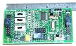
The ADS1256EVM, shown in Figure 1, is an evaluation module built to the TI Modular EVM System
specification. It can be connected to any Modular EVM System interface card.
The ADS1256EVM is available as a stand-alone printed circuit board (PCB) or as part of the
ADS1256EVM-PDK, which includes an MMB0 motherboard and software. As a stand-alone PCB, the
ADS1256EVM is useful for prototyping designs and firmware.
Note that the ADS1256EVM has no microprocessor and cannot run software. To connect it to a computer,
some type of interface is required.
If you intend to use the ADS1255 in your application, use the ADS1256EVM for evaluation and test
purposes. The ADS1255 is in a smaller package, and lacks inputs AIN2 through AIN7; otherwise, it is
identical to the ADS1256.
Figure 1. ADS1256EVM
1.3
Built-In Accessories
The ADS1256EVM includes a system clock crystal and a low-noise voltage reference. Both are optional;
you can select an external system clock and an external reference using slide switches.
The +2.5V reference circuit is based on a REF5025 buffered by an OPA350 and filtered by a large
tantalum electrolytic capacitor. While its noise performance is not sufficiently low to allow the ADS1256 to
perform at its lowest noise level at all data rates, the circuit can closely approach this limit, and is
representative of the kind of reference circuit used in many applications.
1.4
Connectors
The ADS1256 device on the ADS1256EVM is connected through four headers: the analog connector, the
serial connector, the power connector, and the GPIO header. This section describes the respective
pinouts and locations for the connectors and header.
The analog connector (J1) carries analog I/O. The ADS1256 has a nine-input multiplexer connected
through pins 1 through 8 and 10. An optional external differential reference can be connected to pins 18
and 20.
The serial connector (J2) carries the ADS1256 serial digital interface, an optional external system clock
signal, and an I2C™ connection to the onboard serial EEPROM.
SBAU090E – November 2003 – Revised November 2018
Submit Documentation Feedback
ADS1256EVM and ADS1256EVM-PDK
Copyright © 2003–2018, Texas Instruments Incorporated
5
�EVM Overview
www.ti.com
The power connector (J3) carries the power supplies. The ADS1256EVM requires a +5V analog supply
and a +1.8V to +3.3V digital supply. The board is designed using a single ground net connected to DGND.
An AGND pin is also provided. Power options are routed through J4, J9, and J10.
The GPIO header (J5) provides a connection to the four GPIO pins on the EVM.
The ADS1256 uses separate supplies for its analog and digital sections. A jumper is inserted in each
supply line. These jumpers allow the current of each supply to be measured independently.
1.5
Controls
The ADS1256EVM is configured using four slide switches and a jumper.
Switches S1 and S2 select the input signal provided to the first four multiplexer inputs on the ADS1256.
Normally you will use the external input, but you can also use the switches to short the inputs together and
to connect the reference voltage to the inputs. Additionally, the latter two positions are useful for
conducting noise and functional tests.
Switch S3 selects the reference input. One position selects the external reference input pins on the analog
connector (J1). The other two positions connect the onboard +2.5V reference in one of two ways: between
ground and the reference, or between the reference and the analog supply.
Switch S4 selects the system clock source for the ADS1256. You can select between the onboard
7.68MHz crystal or an external clock.
All switches and their settings are additionally described in later sections of this user guide.
2
Analog Interface
For maximum flexibility, the ADS1256EVM is designed for easy interfacing to multiple analog sources.
Samtec part numbers SSW-110-22-F-D-VS-K and TSM-110-01-T-DV-P provide a convenient 10-pin, dualrow, header/socket combination at J1. This header/socket provides access to the analog input pins of the
ADS1256. Consult Samtec at www.samtec.com or call 1-800-SAMTEC-9 for a variety of mating connector
options.
Most of the pins on J1 are directly connected, with minimal filtering or protection. Use appropriate caution
when handling these pins. Table 1 summarizes the pinout for analog interface J1.
Table 1. J1: Analog Interface Pinout
6
Pin Number
Pin Name
Standard
Name
Direction
J1.1
AIN0
AN0–
Input
Analog input 1 (switched by S1)
J1.2
AIN1
AN0+
Input
Analog input 0 (switched by S1)
J1.3
AIN2
AN1–
Input
Analog input 3 (switched by S1)
J1.4
AIN3
AN1+
Input
Analog input 2 (switched by S1)
J1.5
AIN4
AN2–
Input
Analog input 4
J1.6
AIN5
AN2+
Input
Analog input 5
J1.7
AIN6
AN3–
Input
Analog input 6
J1.8
AIN7
AN3+
Input
Analog input 7
J1.10
AINCOM
AN4+
Input
Analog input common
J1.18
SYSREFN
REF–
Input
Inverting external reference input
J1.20
SYSREFP
REF+
Input
Noninverting external reference
input
J1.9-J1.19 odd
GND
AGND
Input
Signal ground
ADS1256EVM and ADS1256EVM-PDK
Function
SBAU090E – November 2003 – Revised November 2018
Submit Documentation Feedback
Copyright © 2003–2018, Texas Instruments Incorporated
�Digital Interface
www.ti.com
3
Digital Interface
3.1
Serial Data Interface
The ADS1256EVM is designed to easily interface with multiple control platforms. Samtec part numbers
SSW-110-22-F-D-VS-K and TSM-110-01-T-DV-P provide a convenient 10-pin, dual-row, header/socket
combination at J2. This header/socket provides access to the digital control and serial data pins of the
TSC. Consult Samtec at www.samtec.com or call 1-800-SAMTEC-9 for a variety of mating connector
options.
All logic levels on J2 are 3.3V CMOS, except for the I2C pins, which conform to 3.3V I2C rules.
Some pins on J2 have weak pullup resistors. These resistors provide default settings for many of the
control pins. Most pins on J2 correspond directly to ADS1256 pins. See the ADS1256 product data sheet
for complete details on these pins. Table 2 describes the J2 serial interface pins.
Table 2. J2: Serial Interface Pins
3.2
Pin Number
Pin Name
Standard
Name
Direction
Pulldown
J2.1
—
CNTL
—
None
Unused
J2.2
—
GPIO0
—
None
Unused
Function
J2.3
SCLK
CLKX
Input
None
Serial clock input
J2.4
DGND
DGND
I/O
Power
Digital ground
J2.5
—
CLKR
—
None
Unused
J2.6
—
GPIO1
—
None
Unused
J2.7
CS
FSX
Input
None
Chip select (via J8)
J2.8
—
GPIO2
—
None
Unused
J2.9
—
FSR
—
None
Unused
J2.10
DGND
DGND
I/O
Power
Digital ground
J2.11
DIN
DX
Input
None
Serial data input
J2.12
—
GPIO3
—
None
Unused
Serial data output
J2.13
DOUT
DR
Input
None
J2.14
RESET
GPIO4
Input
Yes
J2.15
DRDY
INT
Output
None
Data ready signal
J2.16
SCL
SCL
I/O
None
I2C clock line
J2.17
EXTCLK
TOUT
Input
None
External system clock input
J2.18
DGND
DGND
I/O
Power
Digital lround
J2.19
SYNC/PDW
N
GPIO5
Input
Yes
J2.20
SDA
SDA
I/O
None
Reset input (via J7)
Synchronization and power
down control pin (via J6)
I2C data line
GPIO
The ADS1256 has four general-purpose I/O (GPIO) pins. One of these pins can also be configured as a
buffered system clock output. This output is typically used to clock additional ADS1255/ADS1256 devices,
but can be used for other purposes as well. The GPIO pins for the ADS1256 are shown in Figure 2. These
pins (from left to right) are D3 to D0.
SBAU090E – November 2003 – Revised November 2018
Submit Documentation Feedback
ADS1256EVM and ADS1256EVM-PDK
Copyright © 2003–2018, Texas Instruments Incorporated
7
�Power Supplies
www.ti.com
Figure 2. GPIO Pins
Each pin is connected to the GPIO header through a 100Ω resistor. 100kΩ pull-downs on each pin protect
the GPIOs when they are configured as inputs, which is the default setting. The GPIO header, J5, carries
the GPIO pins for the ADS1256.
The GPIO header pinout is described in Table 3.
Table 3. J5: GPIO Header Pins
4
Pin Number
Pin Name
1
D0
GPIO or buffered system clock
output
Function
2
D1
GPIO
3
D2
GPIO
4
D3
GPIO
Power Supplies
J5 is the power-supply input connector. It is used as the primary supply source for the entire EVM. Table 4
lists the configuration details for J2.
Table 4. J5 Configuration: Power-Supply Input
8
Pin No.
Pin Name
J5.1
+VA
Positive analog supply, +5V to
+18V
No
J5.2
–VA
Negative analog supply, -5V to
-18V
No
J5.3
+5VA
Positive analog supply, +5V
Always
J5.4
–5VA
Negative analog supply, -5V
No
J5.5
DGND
Digital ground
Optional connection to
AGND through J10
J5.6
AGND
Analog ground
Ground
J5.7
+1.8VD
Positive digital supply, +1.8V
Digital supply; select
using J9
Positive digital supply
No
Positive digital supply, +3.3V
Digital supply; select
using J10
Positive digital supply, +5V
No
J5.8
VD1
J5.9
+3.3VD
J5.10
+5VD
ADS1256EVM and ADS1256EVM-PDK
Function
Required
SBAU090E – November 2003 – Revised November 2018
Submit Documentation Feedback
Copyright © 2003–2018, Texas Instruments Incorporated
�Power Supplies
www.ti.com
4.1
Power Options
There are six jumpers on the ADS1256EVM, arranged in a single jumper block of seven rows, each of
which can be shorted. (In the schematic, J4, J9, and J10 are all combined to make this single block). The
pinout of this jumper block is shown in Figure 3.
Figure 3. Jumper Block
J4 connects AVDD from the +5V from the power-supply header, J3. J4 also connects the DVDD supply to
the ADS1256 device. DVDD can be set to 1.8V with J9, or to 3.3V with pins 1 and 2 of J10. Pins 3 and 4,
5 and 6, are used to set the ground of the EVM.
Pinouts and connections can all viewed in the schematic and the layout plots at the end of this user guide.
4.1.1
J4 Pins 1-2: ADS1256 Analog Power Supply
This jumper is used to measure the current of the ADS1256 analog power supply. For normal operation,
this jumper should be shorted.
4.1.2
J4 Pins 3-4: ADS1256 Digital Power Supply
Use this jumper to measure the current of the ADS1256 digital power supply. For normal operation, this
jumper should be shorted. The voltage of the digital supply is chosen by the jumper on pins 5-6 (1.8V) or
7-8 (3.3V).
4.1.3
J9 Pins 1-2: Select 1.8V Digital Supply Voltage
These pins select 1.8V for the digital supply voltage. If this selection is used, do not populate pins 7-8.
4.1.4
J10 Pins 1-2: Select 3.3V Digital Supply Voltage
These pins select 3.3V for the digital supply voltage. If this selection is used, do not populate pins 5-6.
4.1.5
J10 Pins 3-4: DGND Select
Shorting this jumper connects the ADS1256EVM ground net to DGND.
SBAU090E – November 2003 – Revised November 2018
Submit Documentation Feedback
ADS1256EVM and ADS1256EVM-PDK
Copyright © 2003–2018, Texas Instruments Incorporated
9
�Voltage Reference
4.1.6
www.ti.com
J10 Pins 5-6: AGND Select
Shorting this jumper connects the ADS1256EVM ground net to AGND. For normal operation, J4.1-2, J4.34, and J4.9-10 must be connected (either directly or through an ammeter); either J4.5-6 or J4.7-8 must be
connected, and either (or both) of J4.11-12 and J4.13-14 must be connected, as well. Otherwise, the
board will not function. Refer to Table 5 for details.
Table 5. J4, J9, and J10 Configuration: Power Options
5
Row
Name
1-2
ADC AVDD
AVDD supply current measurement point for the
ADC. Must be connected for operation.
Function
3-4
ADC AVSS
AVSS supply current measurement point for the
ADC. Must be connected for operation.
5-6
1.8V select
When shorted, DVDD is sourced from the 1.8V
power-supply input pin. Should not be connected at
the same time as 7-8.
7-8
3.3V select
When shorted, DVDD is sourced from the 3.3V
power-supply input pin. Should not be connected at
the same time as 5-6.
9-10
ADCDVDD
DVDD supply current measurement point for the
ADC. Must be connected for operation.
11-12
DGND
Connects DGND to board ground.
13-14
AGND
Connects AGND to board ground.
Voltage Reference
The ADS1256EVM has several reference options that can be selected by switch S3. First, there are
connections to apply an external reference voltage to the analog input header. The user can apply a
reference voltage to J1.18 and J1.20 in order to set the reference.
The ADS1256 also has a buffered REF5025 on board. This 2.5V reference can also be selected by switch
S3. VRN to VRP can be set from AGND to 2.5V or from 2.5V to AVDD. Figure 4 illustrates how switch S3
appears on the board. A description of switch S3 is provided in Table 6.
Figure 4. Switch S3
10
ADS1256EVM and ADS1256EVM-PDK
SBAU090E – November 2003 – Revised November 2018
Submit Documentation Feedback
Copyright © 2003–2018, Texas Instruments Incorporated
�Clock Source
www.ti.com
Table 6. Reference Input Select Switch
Board Marking
Switch Position
Input Source
VRP Connection
EST
Down
External
J1.20
VRN Connection
J1.18
OBH
Middle
Onboard, high commonmode
AVDD
+2.5V
OBL
Up
Onboard, low commonmode
+2.5V
AGND
In the EXT position, J1 pins 18 and 20 are connected to the ADS1256 reference input.
In the OBH position, the analog power supply is connected to the positive reference input, and the
negative reference input is connected to the output of the onboard reference.
In the OBL position, the onboard reference output is connected to the ADS1256 positive reference input
pin, and the negative reference input pin is grounded.
Both OBH and OBL provide a +2.5V reference to the ADS1256. The OBL position corresponds to the
standard method to connect a reference to the ADS1256, and should be used for most measurements.
The OBH position is useful for testing the reference input common-mode sensitivity, which can be
important for ratiometric connections.
6
Clock Source
As shown in Figure 5, switch S4 selects which of the two available clock sources on the ADS1256EVM
will be provided to the ADS1256. Table 7 summarizes the positions of the switch.
Figure 5. Switch S4
Table 7. System Clock Select Switch
Board Marking
Switch Position
Clock Source
XTAL
Left
Onboard 7.68MHz
crystal
EXT
Right
External (J2 pin 17)
SBAU090E – November 2003 – Revised November 2018
Submit Documentation Feedback
ADS1256EVM and ADS1256EVM-PDK
Copyright © 2003–2018, Texas Instruments Incorporated
11
�EVM Operation
7
www.ti.com
EVM Operation
This section provides information on the analog input, digital control, and general operating conditions of
the ADS1256EVM.
7.1
Analog Input
The analog input sources can be applied directly to J1 (top or bottom side). Additionally, switches S1 and
S2 must be set to route the input signals from J1. Otherwise, the inputs are used to measure the
reference or inputs shorted to the reference. Switches S1 and S2 are shown in Figure 6.
Figure 6. Switches S1 and S2
7.1.1
S1: AIN0-1 Input Select
These switches control which lines are routed to the ADS1256 AIN0-AIN1 inputs. Table 8 shows the
positions of these switches.
Table 8. AIN0-1 Input Select Switch (S1)
12
Board Marking
Switch Position
Input Source
AIN0 Connection
EXT
Left
External
J1.2
J1.1
REF
Middle
Reference voltage
+2.5V
AGND
ZERO
Right
Zero (shorted to
reference)
+2.5V
+2.5V
ADS1256EVM and ADS1256EVM-PDK
AIN1 Connection
SBAU090E – November 2003 – Revised November 2018
Submit Documentation Feedback
Copyright © 2003–2018, Texas Instruments Incorporated
�EVM Operation
www.ti.com
In the EXT position, J1 pins 1 and 2 are connected to the ADS1256 AIN1 and AIN0 pins, respectively. In
the REF position, the reference is connected across the ADS1256 AIN0 and AIN1 pins. In the ZERO
position, both AIN0 and AIN1 are connected to the reference. This configuration gives a zero-scale
reading across AIN0 and AIN1.
The REF and ZERO positions are useful for noise tests.
7.1.2
S2: AIN2-3 Input Select
These switches control which lines are routed to the ADS1256 AIN2 through AIN3 inputs. The positions of
the switches are described in Table 9.
Table 9. AIN2-3 Input Select Switch (S2)
Board Marking
Switch Position
Input Source
AIN0 Connection
EXT
Left
External
J1.4
AIN1 Connection
J1.3
REF
Middle
Reference voltage
+2.5V
AGND
ZERO
Right
Zero (shorted to
reference)
+2.5V
+2.5V
In the EXT position, J1 pins 3 and 4 are connected to the ADS1256 AIN3 and AIN2 pins, respectively. In
the REF position, the reference is connected across the ADS1256 AIN2 and AIN3 pins. In the ZERO
position, both AIN2 and AIN3 are connected to the reference. This configuration gives a zero-scale
reading across AIN2 and AIN3.
The REF and ZERO positions are useful for noise tests.
7.1.3
Input Filtering Capacitors
The ADS1256EVM has pads for filtering capacitors on every input pair and for the reference input. Each
input pair has pads for two common-mode capacitors and one differential capacitor.
The ADS1256 has a flexible input multiplexer, so these capacitors do not always function as commonmode and differential signal filters. For example, when measuring a single-ended input, the common-mode
capacitors act to filter the signal.
The ADS1256EVM is shipped with only some of the capacitor pads populated. This configuration allows
the board to be immediately used to measure both differential and single-ended inputs. As shipped, inputs
AIN0 through AIN7 have 10nF differential mode capacitors installed. A differential 1μF capacitor is
connected to the reference near the reference pins.
The input filtering capacitors are in relatively large 1210-size packages, in contrast to most of the other
passives on the board. These capacitors were designed to be large so that you can easily remove them or
replace them with other values. By exercising appropriate care, you can even solder leaded devices to
these large pads.
7.2
Digital Control
The digital control signals can be applied directly to J6 (top or bottom side). The modular ADS1256EVM
can also be connected directly to a DSP or microcontroller interface board, such as the 5-6K Interface or
HPA-MCU Interface boards available from Texas Instruments, or the MMB0 if purchased as part of the
ADS1256EVM-PDK. For a list of compatible interface and/or accessory boards for the EVM or the
ADS1256, see the relevant product folder on the TI web site.
7.3
ADS1256EVM-PDK Power Supply
The analog portion of the ADS1256EVM can either be powered by a 5V source generated via ac adapter,
or by applying the +5VA to the connector on the MMB0 board. The MMB0 board will provide the digital 5V
and 3.3V to the ADS1256EVM. To provide +5VA to the ADS1256EVM from the MMB0 board, make sure
the jumper at J13 (on the MMB0) is closed from +5V to +5VA.
SBAU090E – November 2003 – Revised November 2018
Submit Documentation Feedback
ADS1256EVM and ADS1256EVM-PDK
Copyright © 2003–2018, Texas Instruments Incorporated
13
�EVM Operation
7.4
www.ti.com
Default Jumper Settings and Switch Positions
Figure 7 shows the jumpers and switches found on the EVM and the respective factory default conditions
for each.
Figure 7. ADS1256EVM Default Jumper and Switch Locations
The jumpers on J4 provide a convenient way to measure the current for any of the power-supply currents
AVDD (analog +V power), DVDD (digital power), AVSS (analog –V power), or the ground connections
VGND and DGND. Simply remove the jumper for the appropriate power supply and use a current meter
between the jumper pins. The supply voltage for the digital supply (DVDD) can also be selected to be
either 1.8V or 3.3V; refer to Table 5.
Table 10 and Table 11 provide a list of jumpers and switches found on the EVM and the respective factory
default conditions for each.
Table 10. Default Jumper Positions
Jumper
Default
Jumpers
J4
1-2 and 3-4
J6
2-3
SYNC/PDWN header connection
J7
1-2
RESET header connection
J8
1-2
CS header connection
J9
none
J10
14
Jumper Description
AVDD and DVDD current
measurement connection
+1.8VD connection
1-2, 3-4, and 4-5 +3.3VD, AGND, and DGND
Cconnection
ADS1256EVM and ADS1256EVM-PDK
SBAU090E – November 2003 – Revised November 2018
Submit Documentation Feedback
Copyright © 2003–2018, Texas Instruments Incorporated
�ADS1256EVM-PDK Kit Operation
www.ti.com
Table 11. Default Switch Positions
8
Switch
Default Position
S1
Left
AIN0-1 Input Select Switch
Switch Description
S2
Left
AIN2-3 Input Select Switch
S3
Up
Reference Input Select
S4
Left
System Clock Select Switch
ADS1256EVM-PDK Kit Operation
This section provides information on using the ADS1256EVM-PDK, including setup, program installation,
and program usage. To prepare to evaluate the ADS1256 with the ADS1256EVM-PDK, complete the
following steps:
Step 1. Install the ADCPro software (if not already installed).
Step 2. Install the ADS1256EVM-PDK EVM plug-in software.
Step 3. Set up the ADS1256EVM-PDK.
Step 4. Connect a proper power supply or ac adapter.
Step 5. Complete the NI-VISA™ USB driver installation process.
Step 6. Run the ADCPro software.
Step 7. Complete the Microsoft Windows USB driver installation process.
Each task is described in the subsequent sections of this document.
8.1
Installing the ADCPro Software
CAUTION
Do not connect the ADS1256EVM-PDK before installing the software. Failure to
observe this may cause Microsoft Windows to not recognize the ADS1256EVMPDK.
The latest software is available from Texas Instruments' website at http://www.ti.com/tool/ADS1256EVMPDK. Download the ADCPro Installer from the ADCPro product information page on the TI website. Refer
to the ADCPro User Guide for instructions on installing and using ADCPro.
To install the ADS1256EVM-PDK plug-in, download and run the file: ADS1256evm-pdk-plug-in-1.0.0.exe
from the ADS1256EVM-PDK product folder (1.0.0 is the version number, and increments with software
version releases). Double-click the file to run it; then follow the instructions shown.
Installation for the ADS1256EVM plug-in should be relatively straightforward. The plug-in comes as an
executable file. Once started, the program leads the user through the screens shown in Figure 8 through
Figure 11.
SBAU090E – November 2003 – Revised November 2018
Submit Documentation Feedback
ADS1256EVM and ADS1256EVM-PDK
Copyright © 2003–2018, Texas Instruments Incorporated
15
�ADS1256EVM-PDK Kit Operation
www.ti.com
Figure 8. ADS1256EVM-PDK Setup Wizard
Figure 9. ADS1256EVM-PDK License Agreement
16
ADS1256EVM and ADS1256EVM-PDK
SBAU090E – November 2003 – Revised November 2018
Submit Documentation Feedback
Copyright © 2003–2018, Texas Instruments Incorporated
�ADS1256EVM-PDK Kit Operation
www.ti.com
Figure 10. ADS1256EVM-PDK Installation in Progress
Figure 11. ADS1256EVM-PDK Installation Complete
SBAU090E – November 2003 – Revised November 2018
Submit Documentation Feedback
ADS1256EVM and ADS1256EVM-PDK
Copyright © 2003–2018, Texas Instruments Incorporated
17
�ADS1256EVM-PDK Kit Operation
www.ti.com
The software should now be installed, but the USB drivers may not yet have been loaded by the PC
operating system. This step completes when the ADCPro software is executed; see Section 8.4, Running
the Software and Completing Driver Installation.
8.2
Setting Up the ADS1256EVM-PDK
The ADS1256EVM-PDK contains both the ADS1256EVM and the MMB0 motherboard; however, these
devices are shipped unconnected. Follow these steps to set up the ADS1256EVM-PDK:
Step 1. Unpack the ADS1256EVM-PDK kit.
Step 2. Set the jumpers and switches on the MMB0 as shown in Figure 12.
• Connect +5V and +5VA on jumper block J13 (if +5V is supplied from J14 +5VA).
• Leave +5V and +VA disconnected on jumper block J13.
• If the PDK will be powered from an ac adapter, and used in unipolar mode, connect J12.
If the PDK will be powered through the terminal block or will be used in bipolar mode,
disconnect J12. (See Section 8.3 for details on connecting the power supply.)
Figure 12. MMB0 Initial Configuration
18
ADS1256EVM and ADS1256EVM-PDK
SBAU090E – November 2003 – Revised November 2018
Submit Documentation Feedback
Copyright © 2003–2018, Texas Instruments Incorporated
�ADS1256EVM-PDK Kit Operation
www.ti.com
space
Step 3.
Plug the ADS1256EVM into the MMB0.
CAUTION
Do not misalign the pins when plugging the ADS1256EVM into the MMB0.
Check the pin alignment carefully before applying power to the PDK.
Step 4.
Set the jumpers and switches on the ADS1256EVM as shown in Figure 13 (note that these
settings are the factory-configured settings for the EVM):
• Set jumper block J4 as shown in Figure 7.
• Set the reference source select switches S1 and S2 to the center position.
• Set up jumper block J3 as shown; refer to Figure 7.
Figure 13. Connecting the ADS1256EVM to the MMB0
SBAU090E – November 2003 – Revised November 2018
Submit Documentation Feedback
ADS1256EVM and ADS1256EVM-PDK
Copyright © 2003–2018, Texas Instruments Incorporated
19
�ADS1256EVM-PDK Kit Operation
8.2.1
www.ti.com
About the MMB0
The MMB0 is a Modular EVM System motherboard. It is designed around the TMS320VC5507, a DSP
from Texas Instruments that has an onboard USB interface. The MMB0 also has 16MB of SDRAM
installed.
The MMB0 is not sold as a DSP development board, and it is not available separately. TI cannot offer
support for the MMB0 except as part of an EVM kit. For schematics or other information about the MMB0,
contact Texas Instruments.
8.3
Connecting the Power Supply
The ADS1256EVM-PDK can be operated with a unipolar +5V supply or a bipolar ±5V supply.
If the ADS1256EVM-PDK is to be operated in unipolar mode only, either an ac adapter or a lab power
supply can be used. If the ADS1256EVM-PDK is to be operated in bipolar mode, a ±5V power supply
must be connected; an ac adapter cannot be used.
When the MMB0 DSP is powered properly, LED D2 glows green. The green light indicates that the 3.3V
supply for the MMB0 is operating properly. (It does not indicate that the EVM power supplies are
operating properly.)
8.3.1
Connecting an AC Adapter
An ac adapter can be connected to barrel jack J2 on the MMB0. J2 is located next to the USB connector.
Refer to the External Wall-Adapter Power-Supply Requirements section.
When an ac adapter is used, the ADS1256EVM cannot be used in bipolar mode.
Jumper J12 on the MMB0 connects a wall-mounted power supply to the board. To use the wall-mount
supply, J12 must be shorted, refer to Figure 14.
Figure 14. MMB0 Powered From AC Adapter
20
ADS1256EVM and ADS1256EVM-PDK
SBAU090E – November 2003 – Revised November 2018
Submit Documentation Feedback
Copyright © 2003–2018, Texas Instruments Incorporated
�ADS1256EVM-PDK Kit Operation
www.ti.com
8.3.1.1
External Wall-Adapter Power-Supply Requirements
The external wall-adapter power-supply requirements are as follows:
• Output voltage: 6 VDC to 9 VDC
• Maximum output current: ≥ 500 mA
• Output connector: barrel plug (positive center), 2.0-mm I.D. × 5.5-mm O.D. (9-mm insertion depth)
NOTE: Use an external power supply that complies with applicable regional safety standards; for
example, UL, CSA, VDE, CCC, PSE, and so forth.
8.3.2
Connecting a Laboratory Power Supply
A laboratory power supply can be connected through terminal block J14 on the MMB0, as shown in
Figure 15. Both unipolar and bipolar configurations are supported.
To
•
•
•
use a unipolar lab power supply configuration:
Disconnect J12 on the MMB0.
Connect a +5V dc supply to the +5VD terminal on J14.
Connect ground of the dc supply to the GND terminal on J14.
For bipolar mode, also connect a –5V dc supply to the –5VA terminal on J14. It is not necessary to
connect a +5V dc supply voltage to the +5VA terminal on J14 if the +5V/+5VA position on J13 is shorted.
Figure 15. MMB0 Configured for Lab Power Supply
SBAU090E – November 2003 – Revised November 2018
Submit Documentation Feedback
ADS1256EVM and ADS1256EVM-PDK
Copyright © 2003–2018, Texas Instruments Incorporated
21
�ADS1256EVM-PDK Kit Operation
8.4
www.ti.com
Running the Software and Completing Driver Installation
NOTE: The software is continually under development. These instructions and screen images are
current at the time of this writing, but may not exactly match future releases.
The program for evaluating the ADS1256EVM-PDK is called ADCPro. This program uses plug-ins to
communicate with the EVM. The ADS1256EVM-PDK plug-in is included in the ADS1256EVM-PDK
package.
The program currently runs only on Microsoft Windows platforms of Windows XP; Windows Vista and
Windows 7 are NOT supported.
If this is the first time installing ADCPro and plug-ins, follow these procedures to run ADCPro and
complete the necessary driver installation. Make sure the ADCPro software and device plug-in software
are installed from the CD-ROM as described in Installing the ADCPro Software.
8.4.1
NI-VISA USB Device Driver Installation
1. After the ADCPro software is installed, apply power to the PDK and connect the board to an available
PC USB port.
2. The computer should recognize new hardware and begin installing the drivers for the hardware.
Figure 16 through Figure 19 are provided for reference to show the installation steps.
• For the first screen (Figure 16), it is not necessary to search for the software; it has already been
installed to your PC.
• For the remaining steps, accept the default settings.
Figure 16. NI-VISA Driver Installation Wizard, Screen 1
22
ADS1256EVM and ADS1256EVM-PDK
SBAU090E – November 2003 – Revised November 2018
Submit Documentation Feedback
Copyright © 2003–2018, Texas Instruments Incorporated
�ADS1256EVM-PDK Kit Operation
www.ti.com
Figure 17. NI-VISA Driver Installation Wizard, Screen 2
Figure 18. NI-VISA Driver Installation Wizard, Screen 3
SBAU090E – November 2003 – Revised November 2018
Submit Documentation Feedback
ADS1256EVM and ADS1256EVM-PDK
Copyright © 2003–2018, Texas Instruments Incorporated
23
�ADS1256EVM-PDK Kit Operation
www.ti.com
Figure 19. NI-VISA Driver Installation Wizard, Screen 4
24
ADS1256EVM and ADS1256EVM-PDK
SBAU090E – November 2003 – Revised November 2018
Submit Documentation Feedback
Copyright © 2003–2018, Texas Instruments Incorporated
�ADS1256EVM-PDK Kit Operation
www.ti.com
This should complete the installation of the NI-VISA drivers. You can verify proper installation by opening
the Device Manager and locating the drivers as shown in Figure 20.
Figure 20. NI-VISA Driver Verification Using Device Manager
8.4.2
USBStyx Driver Installation
1. Start the software by selecting ADCPro from the Windows Start menu. The screen shown in Figure 21
appears.
Figure 21. ADCPro Software Start-up Display Window
SBAU090E – November 2003 – Revised November 2018
Submit Documentation Feedback
ADS1256EVM and ADS1256EVM-PDK
Copyright © 2003–2018, Texas Instruments Incorporated
25
�ADS1256EVM-PDK Kit Operation
www.ti.com
space
2. Select ADS1256EVM from the EVM drop-down menu. The ADS1256EVM-PDK plug-in appears in the
left pane, as Figure 22 shows.
Figure 22. ADS1256EVM-PDK Plug-In Display Window
3. The ADS1256EVM-PDK plug-in window has a status area at the top of the screen. When the plug-in is
first loaded, the plug-in searches for the board. You will see a series of messages in the status area
indicating this action.
4. If you have not yet loaded the operating system drivers, Windows will display the Windows Install New
Driver Wizard sequence (illustrated in Figure 23 through Figure 27). Accept the default settings.
NOTE: During the driver installation, a message may appear indicating the firmware load has
TIMED OUT. Click OK and continue driver installation. The plug-in will attempt to download
the firmware again once the driver installation completes.
26
ADS1256EVM and ADS1256EVM-PDK
SBAU090E – November 2003 – Revised November 2018
Submit Documentation Feedback
Copyright © 2003–2018, Texas Instruments Incorporated
�ADS1256EVM-PDK Kit Operation
www.ti.com
Figure 23. Install New Driver Wizard Screen 1
Figure 24. Install New Driver Wizard Screen 2
SBAU090E – November 2003 – Revised November 2018
Submit Documentation Feedback
ADS1256EVM and ADS1256EVM-PDK
Copyright © 2003–2018, Texas Instruments Incorporated
27
�ADS1256EVM-PDK Kit Operation
www.ti.com
Figure 25. Install New Driver Wizard Screen 3
Figure 26. Install New Driver Wizard Screen 4
28
ADS1256EVM and ADS1256EVM-PDK
SBAU090E – November 2003 – Revised November 2018
Submit Documentation Feedback
Copyright © 2003–2018, Texas Instruments Incorporated
�ADS1256EVM-PDK Kit Operation
www.ti.com
Figure 27. Install New Driver Wizard Screen 5
5. Once Windows finishes installing the software driver, the plug-in downloads the firmware to the MMB0.
The status area will display Connected to EVM when the device is connected and ready to use. If the
firmware does not load properly, you can try resetting the MMB0 by pressing Reset and then reloading
the plug-in.
Verify the proper installation of the USBStyx driver using the Device Manager. Note that the first driver
item, NI-VISA USB Devices, disappears and a new item, LibUSB-Win32 Devices appears, as Figure 28
shows.
Figure 28. USBStyx Driver Verification Using Device Manager
The driver installation wizard sequence should not appear again, unless you connect the board to a
different USB port
SBAU090E – November 2003 – Revised November 2018
Submit Documentation Feedback
ADS1256EVM and ADS1256EVM-PDK
Copyright © 2003–2018, Texas Instruments Incorporated
29
�Evaluating Performance with the ADCPro Software
9
www.ti.com
Evaluating Performance with the ADCPro Software
The evaluation software is based on ADCPro, a program that operates using a variety of plug-ins. (The
ADS1256EVM plug-in is installed as described in the installation section, Section 8.)
To use ADCPro, load an EVM plug-in and a test plug-in. To load an EVM plug-in, select it from the EVM
menu. To load a test plug-in, select it from the Test menu. To unload a plug-in, select the Unload option
from the corresponding menu.
Only one of each kind of plug-in can be loaded at a time. If you select a different plug-in, the previous
plug-in is unloaded.
9.1
Using the ADS1256EVM-PDK Plug-in
The ADS1256EVM-PDK plug-in for ADCPro provides complete control over all settings of the ADS1256. It
consists of a tabbed interface (see Figure 22), with different functions available on different tabs. These
controls are described in this section.
You can adjust the ADS1256EVM settings when you are not acquiring data. During acquisition, all
controls are disabled and settings may not be changed. When you change a setting on the ADS1256EVM
plug-in, the setting is immediately updated on the board.
If you unload and reload the plug-in, the software attempts to load settings from the board.
Settings on the ADS1256EVM correspond to settings described in the ADS1256 product data sheet; see
the ADS1256 data sheet (available for download at www.ti.com) for details.
In the upper left corner, the Averages control sets the ADS1256 averaging mode. This control may be set
to 1, 4, 16, or 64. Note that this is a setting for the ADS1256 device itself; no software averaging is done in
the ADS1256EVM-PDK plug-in.
The PGA pull-down menu controls the PGA gain in the ADS1256.
Because the effective data rate of the ADS1256 depends upon the settings of the multiplexer mode,
clocks, switch time delay, chopping, and averages, the Effective Data Rate indicator in the upper right
corner of the plug-in interface is always visible and updates whenever a setting that affects the data rate
changes.
The previous controls are all found at the top of the ADS1256EVM plug-in and shown in Figure 29.
Figure 29. ADS1256EVM-PDK Plug-In Averages, PGA Gain, and Effective Data Rate Controls
30
ADS1256EVM and ADS1256EVM-PDK
SBAU090E – November 2003 – Revised November 2018
Submit Documentation Feedback
Copyright © 2003–2018, Texas Instruments Incorporated
�Evaluating Performance with the ADCPro Software
www.ti.com
9.1.1
MUX Tab
The first tab of the ADS1256EVM plug-in is the MUX tab. In the tab, two columns of push buttons are
used to select the positive and negative inputs for ADS1256. This selection, combined with switches S1
and S2, selects the measurement for the inputs applied to the analog interface J1. The MUX tab is shown
in Figure 30.
Figure 30. MUX Tab
SBAU090E – November 2003 – Revised November 2018
Submit Documentation Feedback
ADS1256EVM and ADS1256EVM-PDK
Copyright © 2003–2018, Texas Instruments Incorporated
31
�Evaluating Performance with the ADCPro Software
9.1.2
www.ti.com
Clocks Tab
The next tab is the Clocks tab, as shown in Figure 31. This tab controls the master clock of the
ADS1256EVM. Enter the master clock frequency in the Clock In window. The clock source can be
selected from between the EVM onboard crystal and the MMB0. The DO/CLKOUT rate can be set by the
Clock Out Rate pull-down menu. There are options to set CLKOUT to fCLKIN, fCLKIN/2, fCLKIN/4, or to turn it off.
Figure 31. Clocks Tab
32
ADS1256EVM and ADS1256EVM-PDK
SBAU090E – November 2003 – Revised November 2018
Submit Documentation Feedback
Copyright © 2003–2018, Texas Instruments Incorporated
�Evaluating Performance with the ADCPro Software
www.ti.com
9.1.3
GPIO Tab
The GPIO tab is used to control the GPIO pins (D0 through D3) on the ADS1256. Four switches are used
to select the GPIO mode (input or output). If the pin is selected as an output, a push button is used to set
the output to be either high or low. If the pin is selected as an input, the Read Inputs button read the
inputs and an indicator light shows if the input is high or low. Figure 32 illustrates the GPIO tab.
Figure 32. GPIO Tab
SBAU090E – November 2003 – Revised November 2018
Submit Documentation Feedback
ADS1256EVM and ADS1256EVM-PDK
Copyright © 2003–2018, Texas Instruments Incorporated
33
�Evaluating Performance with the ADCPro Software
9.1.4
www.ti.com
Power and Reference Tab
The Power & Ref tab selects the reference input, the sensor detect magnitude, and the standby condition.
The VREF Source window has three pushbuttons that select the reference source and should correspond
with the reference setting for switch S3. OBL sets the reference input from AGND to VREF, while OBH
sets the reference input from VREF to AVDD. External sets the input from VREF– to VREF+ on the
analog input header. If the user applies an external reference, the Vref window can be set to calculate the
voltage when using the Multichannel Scope test plug-in.
The ADS1256 has sensor detect current sources that can be used to detect a burned out sensor. These
current sources are applied to the inputs internal to the ADC. The sensor detect current sources can be
set to 0.5mA, 2mA, 10mA, or turned off through using a series of pushbuttons.
To reduce the operating current when the device is not in use, the ADS1256 can be put into standby
mode with a pushbutton labeled Standby. Pressing the Wakeup button releases the ADS1256 from this
mode.
The Power & Ref tab is illustrated in Figure 33.
Figure 33. Power & Ref Tab
34
ADS1256EVM and ADS1256EVM-PDK
SBAU090E – November 2003 – Revised November 2018
Submit Documentation Feedback
Copyright © 2003–2018, Texas Instruments Incorporated
�Evaluating Performance with the ADCPro Software
www.ti.com
9.1.5
Calibration Tab
The Cal tab (as Figure 34 illustrates) controls the calibration of the offset and gain error of the ADS1256.
Pressing a pushbutton at the top of the tab runs a self-calibration of the device. Four buttons allow four
other calibration options: Self Offset Calibration, System Offset Calibration, Self Gain Calibration, and
System Gain Calibration.
At the bottom of the tab, there are four windows that allow for manually entering and reading back
calibration values for the offset calibration register and the gain calibration register. The Set button enters
the value in the window into the calibration register, while the Read button reads the current calibration
register value.
Figure 34. Cal Tab
SBAU090E – November 2003 – Revised November 2018
Submit Documentation Feedback
ADS1256EVM and ADS1256EVM-PDK
Copyright © 2003–2018, Texas Instruments Incorporated
35
�Evaluating Performance with the ADCPro Software
9.1.6
www.ti.com
About Tab
The About tab displays information about the EVM and software, as Figure 35 shows.
The Plugin Version and Firmware Version indicators show the version numbers of the plug-in and
firmware code, respectively. The Notes indicator may show relevant notes about the plug-in or firmware
code, if there are any.
Figure 35. EVM Software About Tab
36
ADS1256EVM and ADS1256EVM-PDK
SBAU090E – November 2003 – Revised November 2018
Submit Documentation Feedback
Copyright © 2003–2018, Texas Instruments Incorporated
�Evaluating Performance with the ADCPro Software
www.ti.com
9.1.7
Collecting Data
Once you have configured the ADS1256 for your test scenario, pressing the ADCPro Acquire button
starts the collection of the number of datapoints specified in the Test plug-in Block Size control. The
ADS1256EVM-PDK plug-in disables all the front panel controls while acquiring, and displays a progress
bar as shown in Figure 36.
Figure 36. Software Progress Indicator
For more information on testing analog-to-digital converters in general and using ADCPro and Test plugins, refer to the ADCPro User Guide.
9.2
Troubleshooting
If ADCPro stops responding while the ADS1256EVM-PDK is connected, try unplugging the power supply
from the PDK. Unload and reload the plug-in before reapplying power to the PDK.
SBAU090E – November 2003 – Revised November 2018
Submit Documentation Feedback
ADS1256EVM and ADS1256EVM-PDK
Copyright © 2003–2018, Texas Instruments Incorporated
37
�Schematics and Layout
10
www.ti.com
Schematics and Layout
A schematic for the ADS1256EVM is appended to this user's guide. The bill of materials is provided in
Table 12. Figure 37 through Figure 40 illustrate the ADS1256EVM printed circuit board (PCB) layouts.
Table 12. ADS1256EVM Bill of Materials
Item No
Qty
Value
Ref Des
1
1
10kΩ
R1
1/10W 5% chip resistor
Panasonic
ERJ-3GEYJ103V
2
2
47kΩ
R2, R3
1/10W 5% chip resistor
Panasonic
ERJ-3GEYJ473V
3
3
100Ω
RA1, RA2, RA3
Resistor array, eight terminal,
four resistor
CTS
744C083101JPTR
4
1
100kΩ
RA4
Resistor array, eight terminal,
four resistor
CTS
744C083104JPTR
5
2
18pF
C21. C22
50V ceramic chip capacitor, ±5%,
C0G
TDK
C1608C0G1H180JT
6
2
0.1μF
C23, C24
16V ceramic chip capacitor,
±10%, X7R
TDK
C1608X7R1C104KT
7
2
1μF
C3, C18
16V ceramic chip, ±10%, X7R
TDK
C2012X7R1C105KT
8
2
4.7μF
C19, C20
6.3V ceramic chip ±20%, X5R
TDK
C2012X5R0J475KT
9
1
100μF
C4
10
4
10nF
C1, C2, C7, C10
11
1
U1
Analog to digital converter
Texas Instruments
ADS1256IDB
12
1
U2
Operational amplifier
Texas nstruments
OPA350UA
13
1
U3
+2.5V voltage reference
Texas Instruments
REF5025ID
14
1
U4
15
2
J1A, J2A
20 pin SMT plug
Samtec
TSM-110-01-L-DV-P
16
2
J1B, J2B
20 pin SMT socket
Samtec
SSW-110-22-F-D-VS-K
17
1
J3A
10 pin SMT plug
Samtec
TSM-105-01-L-DV-P
18
1
J3B
10 pin SMT socket
Samtec
SSW-105-22-F-D-VS-K
19
3
J6, J7, J8
Three-position header, 0 .1
spacing
Samtec
TSW-103-07-L-S
20
1
J5
Four-position header, 0 .1in
spacing
Samtec
TSW-104-07-L-S
21
1
J4
2 x 2 position header, 0.1in
spacing
Samtec
TSW-102-07-L-D
22
1
J10
2 x 3 position header, 0.1in
spacing
Samtec
TSW-103-07-L-D
23
1
N/A
ADS1256EVM PWB
Texas Instruments
6450840
24
3
S1, S2, S3
DP3T Switch
E-Switch
EG2305A
25
1
S4
SPDT Switch
NKK
26
1
X1
Crystal, SMD
Citizen
HCM49-7.680MABJ-UT
27
8
N/A
Jumper top
Samtec
SNT-100-BK-T
1×2 Position header, 0.1”
spacing
Samtec
TSW-102-07-L-S
Not
Installed
Not
Installed
38
Description
Vendor
10V low ESR tantalum capacitor,
±20%
Kemet
16V PPS chip capacitor, ±2%
Panasonic
2
Microchip
256K I C EEPROM
Part No
T520D107M010ATE055
ECH-U1C103GX5
24AA256-I/SN
SS12SDP2
C5, C6, C8, C9, C11,
C12,C13, C14, C15,
C16, C17
1
J9
ADS1256EVM and ADS1256EVM-PDK
SBAU090E – November 2003 – Revised November 2018
Submit Documentation Feedback
Copyright © 2003–2018, Texas Instruments Incorporated
�Schematics and Layout
www.ti.com
Figure 37. ADS1256EVM PCB: Top-Side Image
Figure 38. ADS1256EVM PCB: Layer 1
Figure 39. ADS1256EVM PCB: Layer 2
Figure 40. ADS1256EVM PCB: Bottom-Side Image
SBAU090E – November 2003 – Revised November 2018
Submit Documentation Feedback
ADS1256EVM and ADS1256EVM-PDK
Copyright © 2003–2018, Texas Instruments Incorporated
39
�Schematics and Layout
www.ti.com
S1
ESW_EG2305A
C14
DNP
J8
CS
J7
RESET
R3
DVDD
AIN0
AIN1
C10
C11
DNP
AVDD
AVDD
C23
R1
VIN
VOUT
TEMP
GND TRIM
5
7
U2
OPA350
1
3
4
100U TA C4
C5
DNP
C5: OPTIONAL MLCC REF CAP
C3
1U 16V X7R
D0C
D1C
D2C
D3C
C21
18P
C22
18P
1
2
3
4
HEADER-4
RA4
100K
DVDD
U4
1
2
3
7
A0
A1
A2
WP
VCC
SDA
SCL
GND
8
5
6
4
DVDD
1
3
5
7
9
2
JPR-2X1
J10
1
3
5
J3
AVDD
2
4
1
+1.8VIN
VOLTAGE REFERENCE FILTER CAPACITORS C3-C5
C4: 100UF LOW ESR TANTALUM
KEMET "KO-CAP" T520D107M010AS4350
J5
D0
D1
D2
D3
JPR-2X2
J9
+3.3VIN
AGNDIN
DGNDIN
REF5025
INSTALL EITHER C4 OR C5
SERIALHDR
J6
SYNC/PDWN
NKK_SS12SDP2
RA3
100
X1
7.68MHZ
2
4
6
8
10
12
14
16
18
20
GPIO0
DGND
GPIO1
GPIO2
DGND
GPIO3
GPIO4
SCL
DGND
SDA
MCP_24AA256-I/SN
6
C3: 1UF MLCC, 0805 PKG
MURATA
KEMET C0805C105K4RACTU
S4
CNTL
CLKX
CLKR
FSX
FSR
DX
DR
INT
TOUT
GPIO5
AVDD
3
6
CLKIN
DVDD
1
3
5
7
9
11
13
15
17
19
J4
10K
U3
INT
TOUT
GPIO5
4U7
C12
DNP
FSX
100
RA2
EXTCLK 100
C20
C13
DNP
2
0.1uF
C19
4U7
S3
ESW_EG2305A
J2
DX
DR
CS
SCLK
DIN
DOUT
DRDY
SYNC/PDWN
RESET
ADS1256
C18
1U
C24
0.1uF
10nF
16
20
24
23
22
21
14
15
25
26
27
28
19
18
17
SDA
2
4
6
8
10
12
14
16
18
20
AN0+
AN1+
AN2+
AN3+
AN4+
AN5+
AN6+
AN7+
REFREF+
VRP
VRN
ADCAVDD
C9
DNP
REFREF+
AN0AN1AN2AN3AGND
AGND
AGND
VCOM
AGND
AGND
AIN4
AIN5
AIN6
AIN7
AINCOM
DVDD
CS
SCLK
DIN
DOUT
DRDY
SYNC/PDWN
RESET
D0/CLKOUT
D1
D2
D3
XTAL1/CLKIN
XTAL2
DGND
AVDD
VRP
VRN
AIN0
AIN1
AIN2
AIN3
AIN4
AIN5
AIN6
AIN7
AINCOM
AGND
XTAL2
10nF
ANALOGHDR
2
3
4
1
4
3
6
7
8
9
10
11
12
13
5
2
C8 DNP
J1
1
3
5
7
9
11
13
15
17
19
CLKX
ADCDVDD
C7
DNP
AVDD
47k
RA1
U1
C17
DNP
C6
R2
1
2
3
C16
DNP
AIN2
AIN3
AN1+
AN1-
OBREF
C2
10nF
3
2
3
2
1
47k
GPIO4 1
C15
DNP
S2
ESW_EG2305A
SCL
AN0+
AN0-
C1
10nF
2
4
6
JPR-2X3
+VA
-VA
+5VA
-5VA
DGND AGND
+1.8VD
VD1
+3.3VD +5VD
2
4
6
8
10
POWERHDR
C5: 22UF MLCC
MURATA
KEMET
PANASONIC
Figure 41. Schematic
40
ADS1256EVM and ADS1256EVM-PDK
SBAU090E – November 2003 – Revised November 2018
Submit Documentation Feedback
Copyright © 2003–2018, Texas Instruments Incorporated
�Revision History
www.ti.com
Revision History
NOTE: Page numbers for previous revisions may differ from page numbers in the current version.
Changes from D Revision (May 2016) to E Revision ...................................................................................................... Page
•
Added Schematic image ................................................................................................................ 40
Changes from C Revision (July 2010) to D Revision ..................................................................................................... Page
•
•
Updated software download links in the Installing the ADCPro Software section. .............................................. 15
Added External Wall-Adapter Power-Supply Requirements section. ............................................................. 21
SBAU090E – November 2003 – Revised November 2018
Submit Documentation Feedback
Copyright © 2003–2018, Texas Instruments Incorporated
Revision History
41
�IMPORTANT NOTICE AND DISCLAIMER
TI PROVIDES TECHNICAL AND RELIABILITY DATA (INCLUDING DATA SHEETS), DESIGN RESOURCES (INCLUDING REFERENCE
DESIGNS), APPLICATION OR OTHER DESIGN ADVICE, WEB TOOLS, SAFETY INFORMATION, AND OTHER RESOURCES “AS IS”
AND WITH ALL FAULTS, AND DISCLAIMS ALL WARRANTIES, EXPRESS AND IMPLIED, INCLUDING WITHOUT LIMITATION ANY
IMPLIED WARRANTIES OF MERCHANTABILITY, FITNESS FOR A PARTICULAR PURPOSE OR NON-INFRINGEMENT OF THIRD
PARTY INTELLECTUAL PROPERTY RIGHTS.
These resources are intended for skilled developers designing with TI products. You are solely responsible for (1) selecting the appropriate
TI products for your application, (2) designing, validating and testing your application, and (3) ensuring your application meets applicable
standards, and any other safety, security, regulatory or other requirements.
These resources are subject to change without notice. TI grants you permission to use these resources only for development of an
application that uses the TI products described in the resource. Other reproduction and display of these resources is prohibited. No license
is granted to any other TI intellectual property right or to any third party intellectual property right. TI disclaims responsibility for, and you
will fully indemnify TI and its representatives against, any claims, damages, costs, losses, and liabilities arising out of your use of these
resources.
TI’s products are provided subject to TI’s Terms of Sale or other applicable terms available either on ti.com or provided in conjunction with
such TI products. TI’s provision of these resources does not expand or otherwise alter TI’s applicable warranties or warranty disclaimers for
TI products.
TI objects to and rejects any additional or different terms you may have proposed. IMPORTANT NOTICE
Mailing Address: Texas Instruments, Post Office Box 655303, Dallas, Texas 75265
Copyright © 2022, Texas Instruments Incorporated
�