User's Guide
SBAU261B – May 2016 – Revised April 2017
ADS127L01EVM
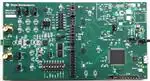
Figure 1. ADS127L01EVM
The ADS127L01EVM is an evaluation module that provides hardware and software support for evaluation
of the ADS127L01 delta-sigma ADC. The EVM utilizes the TM4C1294NCPDT processor to communicate
with the ADC via SPI and provide communication with a PC over USB interface. The EVM also includes a
software application that runs on a PC to allow for register manipulation and data collection from the ADC.
Table 1. Related Documentation
Device
Literature Number
ADS127L01
SBAS607
Microsoft, Windows are registered trademarks of Microsoft Corporation.
All other trademarks are the property of their respective owners.
SBAU261B – May 2016 – Revised April 2017
Submit Documentation Feedback
ADS127L01EVM
Copyright © 2016–2017, Texas Instruments Incorporated
1
�www.ti.com
1
2
3
4
5
6
7
Contents
EVM Overview ............................................................................................................... 3
1.1
Description ........................................................................................................... 3
1.2
Requirements ....................................................................................................... 3
1.3
Software Reference ................................................................................................ 3
1.4
Supported Functionality ............................................................................................ 3
Quick Start .................................................................................................................... 5
2.1
Default Jumper and Switch Configuration ....................................................................... 5
2.2
Power Connection .................................................................................................. 6
2.3
Startup................................................................................................................ 6
Hardware Reference ........................................................................................................ 7
3.1
Jumper and Switch Configuration Reference ................................................................... 7
3.2
Headers, Connectors, and Test Points .......................................................................... 8
ADS127L01EVM Software ................................................................................................ 10
4.1
Installing the Software ............................................................................................ 10
4.2
Connecting to the EVM Hardware .............................................................................. 11
4.3
Using the Software With the ADS127L01EVM ................................................................ 12
ADS127L01EVM Hardware ............................................................................................... 15
5.1
Analog Inputs ...................................................................................................... 15
5.2
Hardware Mode Pins ............................................................................................. 16
5.3
ADC Reference .................................................................................................... 17
5.4
Power-Down Mode ................................................................................................ 17
5.5
Digital Inputs ....................................................................................................... 17
5.6
Clock Inputs ........................................................................................................ 18
Power Supply Connections ............................................................................................... 19
6.1
Powering the EVM ................................................................................................ 19
6.2
ADC Power Supplies ............................................................................................. 19
ADS127L01EVM Bill of Materials, PCB Layout, and Schematic ..................................................... 20
7.1
Bill of Materials .................................................................................................... 20
7.2
PCB Layout ........................................................................................................ 26
7.3
Schematic .......................................................................................................... 30
List of Figures
1
ADS127L01EVM ............................................................................................................. 1
2
ADS127L01EVM Default Jumper and Switch Configuration ........................................................... 5
3
Delta-Sigma ADC EvaluaTIon Software Installation Instructions .................................................... 10
4
................................................................
ADS127L01 Device Tab and Register Map ............................................................................
Register Controls for the ADS127L01 ...................................................................................
Hardware Controls for the ADS127L01 Mode Pins ....................................................................
Analog Input Connections (Schematic) .................................................................................
Analog Input Connections (PCB).........................................................................................
Modifications to Bypass Driver Stage ...................................................................................
Hardware Mode Input Controls (Schematic)............................................................................
Hardware Mode Input Controls (PCB) ...................................................................................
Reference Input Selection.................................................................................................
Debug Header for Logic Analyzer (Schematic) ........................................................................
Debug Header for Logic Analyzer (PCB) ...............................................................................
Clock Tree (Schematic) ...................................................................................................
Clock Tree (PCB) ..........................................................................................................
Top Silkscreen ..............................................................................................................
Top Layer (Positive) .......................................................................................................
5
6
7
8
9
10
11
12
13
14
15
16
17
18
19
2
ADS127L01 Device Package Installation Instructions
ADS127L01EVM
11
12
13
13
15
15
15
16
16
17
17
17
18
18
26
26
SBAU261B – May 2016 – Revised April 2017
Submit Documentation Feedback
Copyright © 2016–2017, Texas Instruments Incorporated
�EVM Overview
www.ti.com
20
21
22
23
24
25
26
27
28
29
30
31
32
33
34
.........................................................................................................
Power (Negative) ...........................................................................................................
Bottom Layer (Positive)....................................................................................................
Bottom Silkscreen ..........................................................................................................
Bottom Silkscreen (Mirrored) .............................................................................................
TM4C Main Schematic ....................................................................................................
TM4C Miscellaneous and Power Schematic ...........................................................................
ADS127L01EVM Digital Header Schematic ............................................................................
ADS127L01EVM USB Power Schematic ...............................................................................
ADS127L01EVM External Power Schematic ...........................................................................
ADS127L01EVM Clock Tree Schematic ................................................................................
ADS127L01EVM ADC Main Schematic .................................................................................
ADS127L01EVM ADC Input Driver Schematic.........................................................................
ADS127L01EVM ADC Reference Schematic ..........................................................................
ADS127L01EVM ADC Power Schematic ...............................................................................
Ground (Negative)
1
EVM Overview
1.1
Description
27
27
28
28
29
30
31
32
33
34
35
36
37
38
39
This user guide describes the operation and use of the ADS127L01 evaluation module (ADS127L01EVM).
The ADS127L01 is a 24-Bit, high-speed, wide-bandwidth delta-sigma analog-to-digital converter (ADC) for
precision industrial applications. This platform is intended for evaluating the ADS127L01 performance and
functionality. The ADS127L01EVM kit includes the ADS127L01EVM, USB mini cable, and supporting
software (SW).
This document includes a detailed description of the hardware (HW) and software, bill of materials, and
schematic for the ADS127L01EVM.
Throughout this document, the terms ADS127L01EVM, demonstration kit, evaluation module, and EVM
are synonymous with the ADS127L01EVM. Also, the term GUI is synonymous with Delta-Sigma ADC
EvaluaTIon Software, core application, and EVM software, and Tiva is synonymous with the
TM4C1294NCPDT.
1.2
Requirements
1.2.1
Software Requirements
PC with Microsoft® Windows® 7 or higher operating system.
1.2.2
Hardware Requirements
PC with available USB connection.
1.3
Software Reference
See the Delta-Sigma ADC EvaluaTIon Software User Manual (SBAU260) for the core software
documentation or navigate to File -> About from within the GUI.
1.4
Supported Functionality
1.4.1
Supported Hardware Functionality
•
•
•
Unipolar 3-V analog supply (AVDD)
Unipolar 1.8-V and 3.3-V digital supply (DVDD)
External LVDD supply
SBAU261B – May 2016 – Revised April 2017
Submit Documentation Feedback
ADS127L01EVM
Copyright © 2016–2017, Texas Instruments Incorporated
3
�EVM Overview
•
•
•
•
•
•
•
1.4.2
Fully-differential or single-ended input driver
Hardware control over device mode pins:
– High-resolution (HR), low-power (LP), and very-low-power (VLP) mode
– All OSR [1:0] and FILTER[1:0] settings
SPI and frame-sync interface (frame-sync mode requires external processor)
Digital header for debug or connection to external processor
On-board ADC clock options (CLK): 16 MHz, 8 MHz, 4 MHz
On-board or external ADC reference voltage (REFN always shorted to GND)
Power-down mode
Supported Software Functionality
•
•
•
•
4
www.ti.com
Software control over device mode pins:
– High-resolution (HR), low-power (LP), and very-low-power (VLP) mode
– All OSR [1:0] and FILTER[1:0] settings
SPI mode only
SPI serial interface commands:
– RESET
– START
– STOP
– RDATA
– RREG
– WREG
Does not support:
– Frame-sync master mode or frame-sync slave mode
– STATUS word readback
ADS127L01EVM
SBAU261B – May 2016 – Revised April 2017
Submit Documentation Feedback
Copyright © 2016–2017, Texas Instruments Incorporated
�Quick Start
www.ti.com
2
Quick Start
This section provides a guide to quickly begin using the EVM.
2.1
Default Jumper and Switch Configuration
The EVM should come configured with the settings listed in Table 2 and illustrated in Figure 2.
Table 2. Default Settings
(1)
Jumper
Default Position
JP1
Uninstalled
Comment
Use on-board processor
JP2
Uninstalled
USB-derived supplies enabled
JP3
1-2
AVDD and DVDD derived from regulated USB supply
JP4
N/A
Not populated
JP5
Uninstalled
JP6
1-2
JP7
Uninstalled
JP8
1-2
Enable on-board crystal oscillator (Y1)
CLK = 16 MHz
ADS127L01 powered-on
REXT = 60.4 kΩ
JP9
Installed
JP10
Uninstalled
Internal LDO used for LVDD supply
JP11
1-2
Switch
Default Position
S1
Open
GPIO input pulled high
S2
Open
Tiva RST pulled high
S3
HR = 1
FORMAT = 0
OSR [1:0] = 00
FSMODE = 0 (1)
FILTER [1:0] = 01
Input amplifier enabled (U30)
DVDD = 1.8 V
Comment
High-resolution mode
SPI mode
OSR = 32
Frame-sync slave mode (1)
Wideband 2 filter (transition: 0.4 FDATA to 0.5 FDATA)
Ignored when FORMAT = 0
Figure 2. ADS127L01EVM Default Jumper and Switch Configuration
SBAU261B – May 2016 – Revised April 2017
Submit Documentation Feedback
ADS127L01EVM
Copyright © 2016–2017, Texas Instruments Incorporated
5
�Quick Start
2.2
www.ti.com
Power Connection
The EVM is powered via the USB interface with the PC. Connect the EVM to an available USB port to
power the board.
2.3
Startup
Use the following steps at startup:
1. Install the core application onto your PC.
2. Install the ADS127L01 device package onto your PC.
3. Ensure all jumpers and switches are configured in the default configuration per Table 2 and Figure 2.
4. Connect the EVM to your PC using a USB cable.
5. If prompted, install any required drivers.
6. Start the software on your PC.
NOTE: The EVM has powered on correctly if D4 turns on.
6
ADS127L01EVM
SBAU261B – May 2016 – Revised April 2017
Submit Documentation Feedback
Copyright © 2016–2017, Texas Instruments Incorporated
�Hardware Reference
www.ti.com
3
Hardware Reference
3.1
Jumper and Switch Configuration Reference
Table 3 provides all jumper and switch configuration settings for the EVM.
Table 3. Hardware Item Descriptions
Jumper
Position
JP1
Select on-board vs. external controller (U1 RST)
JP2
JP3
JP4
JP5
JP6
JP7
JP8
JP9
JP10
JP11
Description
Installed
Hold on-board Tiva in reset and disable level shifters to allow external digital interface
Uninstalled
Normal operation with on-board Tiva
Enable USB-derived power supplies (U11 EN)
Installed
USB-derived power supplies disabled
Uninstalled
USB-derived power supplies enabled
Select 5-V supply to derive AVDD_5V and DVDD_3.3V
1-2
AVDD_5V and DVDD_3.3V derived from regulated USB supply (U12)
2-3
Not used
Power-down external supplies (U16 EN)
Installed
External supplies disabled
Uninstalled
External supplies enabled
Disable on-board crystal oscillator Y1 (CLKEN)
Installed
Y1 output is disabled
Uninstalled
Y1 output is enabled
Select ADS127L01 CLK frequency (CLKSEL)
1-2
16 MHz
3-4
8 MHz
5-6
4 MHz
Place ADS127L01 in Power-Down Mode (RESET/PWDN)
Installed
ADS127L01 held in Power-Down Mode
Uninstalled
Normal operation
Select REXT pull-down resistor (U26 REXT)
1-2
60.4 kΩ (HR and LP Mode)
2-3
120 kΩ (VLP Mode)
Select source for ADS127L01 LVDD supply (U26 INTLDO)
Installed
Internal LDO enabled (LVDD sourced from AVDD)
Uninstalled
Internal LDO disabled (LVDD sourced from external supply connected to TP17)
Power-down input driver amplifier (U26 PD)
Installed
Amplifier held in power-down
Uninstalled
Normal operation
Select DVDD supply for ADS127L01 (U26 DVDD)
1-2
DVDD = 1.8 V
2-3
DVDD = 3.3 V
Switch
Position
Description
S1
BSL Mode for Device Firmware Update (DFU)
S2
Closed (on RESET)
Total Tiva FLASH erasure (Tiva enumerates as a DFU device on release)
Open (on RESET)
Normal operation
Reset on-board Tiva controller (U1 RST)
Closed
Tiva held in RESET
Open
Normal operation
SBAU261B – May 2016 – Revised April 2017
Submit Documentation Feedback
ADS127L01EVM
Copyright © 2016–2017, Texas Instruments Incorporated
7
�Hardware Reference
www.ti.com
Table 3. Hardware Item Descriptions (continued)
3.2
Switch
Position
S3
Hardware Mode inputs
Description
Open
Logic ‘1’
Closed
Logic ‘0’
Headers, Connectors, and Test Points
This section provides details for all of the headers, connectors, and test points on the EVM.
3.2.1
JTAG Header (not installed)
The J2 header is provided for programming the on-board processor with firmware updates or user
firmware. Exercise care when using the JTAG since it is possible to erase the EVM firmware and lose
communication with the EVM software. Table 4 describes the J2 header functions.
Table 4. JTAG Header, J2
Function
3.2.2
Signal Name
Pin
Processor RESET Signal
RESET
1
JTAG test data out signal
TDO
2
JTAG test data in signal
TDI
3
JTAG test mode select signal
TMS
4
JTAG test clock signal
TCK
5
Debug UART receive signal
RX
6
Debug UART transmit signal
TX
7
Analog Inputs
Analog input signals can be connected through the SMA connectors (J7 and J9) or through the terminal
block (J8). Table 5 lists the analog input connections.
Table 5. Analog Inputs, J7–J9
Function
3.2.3
SMA Connector
Terminal Block
Analog input to AINN
J7
J8[1]
Analog input to AINP
J9
J8[2]
Test Points
The test points listed in Table 6 may be used to probe on-board voltage supplies or to connect external
voltage supplies. See the ADS127L01EVM Hardware section for any required hardware modifications
when connecting an external supply.
Table 6. Test Points, TP17 – TP24
Function
Test Point
Input Restrictions
ADC Modulator Supply
LVDD
TP17
1.7 V ≤ LVDD ≤ 1.9 V
Input Common-Mode Voltage
VOCM
TP18
0.55 V ≤ VOCM ≤ 1.8 V
ADC Reference Voltage
REFP
TP19
0.5 V ≤ VREF ≤ 3.0 V
2.7 V ≤ AVDD ≤ 3.6 V
ADC Analog Supply
AVDD
TP20
ADC Digital Supply
DVDD
TP21
1.7 V ≤ DVDD ≤ 3.6 V
TP6-10, TP22-24
Connect to external source ground
System Ground
8
Signal Name
GND
ADS127L01EVM
SBAU261B – May 2016 – Revised April 2017
Submit Documentation Feedback
Copyright © 2016–2017, Texas Instruments Incorporated
�Hardware Reference
www.ti.com
3.2.4
Digital Interface Header
Table 7 lists the functions and pin numbers for all signals used on the digital interface header.
Table 7. Digital Interface Header, J3
Function
Processor Side
GPIO Inputs for ADC
Hardware Mode Pins
ADC Side
Pin Number (1)
Pin Number (2)
I2C0_SDA
1
2
FILTER1
I2C0_SCL
3
4
FILTER0
TIVA_16MHz_LT
5
6
TIVA_16MHz
GPIO_4
7
8
FSMODE
GPIO_3
9
10
OSR1
GPIO_2
11
12
OSR0
GPIO_1
13
14
FORMAT
Signal Name
Signal Name
GPIO_0
15
16
HR
IOVDD Supply for Level
Translator (U5)
DIG_VOLT2
17
18
DVDD
GPIO
I2C1_SDA
19
20
DRDY
SPI Port
SPI1_MISO/DATA1
27
28
MISO
SPI1_MOSI/DATA0
29
30
MOSI
SPI1_FS
31
32
CS
SPI1_SCLK
33
34
SCLK
DIG_VOLT3
35
36
DVDD
IOVDD Supply for Level
Translator (U7)
(1)
(2)
Odd numbered pins not included are connected to Tiva inputs whose functionality is not used for this EVM. See Figure 27 for connection
details.
Even numbered pins not included are not connected to the ADS127L01.
3.2.5
Debug Header
The debug header (J6) information is presented in Table 8.
Table 8. Debug Header, J6
Function
Digital Signals for Logic Analyzer or External Processor
(1)
Signal Name
Pin Number (1)
CS
1
SCLK
3
DIN
5
DOUT
7
DRDY
9
Pins 2 – 10 (even) are tied to GND.
SBAU261B – May 2016 – Revised April 2017
Submit Documentation Feedback
ADS127L01EVM
Copyright © 2016–2017, Texas Instruments Incorporated
9
�ADS127L01EVM Software
www.ti.com
4
ADS127L01EVM Software
4.1
Installing the Software
4.1.1
Delta-Sigma ADC EvaluaTIon Software
Download the Delta-Sigma EvaluaTIon Software installer from the ADS127L01EVM tool page and save to
a known folder. Run the installer and follow the on-screen prompts. Note that future software versions may
show slightly different screens.
Figure 3. Delta-Sigma ADC EvaluaTIon Software Installation Instructions
10
ADS127L01EVM
SBAU261B – May 2016 – Revised April 2017
Submit Documentation Feedback
Copyright © 2016–2017, Texas Instruments Incorporated
�ADS127L01EVM Software
www.ti.com
4.1.2
ADS127L01 Device Package
Download the ADS127L01 Device Package installer from the ADS127L01EVM tool page and save to a
known folder. Run the installer and follow the on-screen prompts. Note that future software versions may
show slightly different screens.
Figure 4. ADS127L01 Device Package Installation Instructions
4.2
Connecting to the EVM Hardware
After the Delta-Sigma ADC EvaluaTIon Software and the ADS127L01 Device Package are installed,
ensure that all jumpers and switches are in their default positions per Table 2, and then connect the
hardware with the provided USB mini cable. Start the Delta-Sigma ADC EvaluaTIon Software. The GUI
automatically detects the connected hardware and displays the device register map under the Main tab as
shown in Figure 5.
SBAU261B – May 2016 – Revised April 2017
Submit Documentation Feedback
ADS127L01EVM
Copyright © 2016–2017, Texas Instruments Incorporated
11
�ADS127L01EVM Software
4.3
www.ti.com
Using the Software With the ADS127L01EVM
This section covers the functionality of the ADS127L01 device package only. For more information about
the core application, see the Delta-Sigma ADC EvaluaTIon Software User Manual (SBAU260) for the core
software documentation or navigate to File -> Options from within the GUI.
Upon startup, the GUI scans for the connected hardware. Once the ADS127L01EVM is plugged in, the
welcome screen will refresh to show the ADS127L01 Register Map under the main Device tab as shown
in Figure 5. The Device tab also grants user control over register settings with read/write access (R/W) as
well as the ADS127L01 hardware mode pins. Click the Refresh/Sync button to read back the current value
in all registers and update the register map. Selecting a single register will provide a detailed description
for the current values in the Register Decode Information panel below the register map (see lower half of
Figure 5).
Figure 5. ADS127L01 Device Tab and Register Map
12
ADS127L01EVM
SBAU261B – May 2016 – Revised April 2017
Submit Documentation Feedback
Copyright © 2016–2017, Texas Instruments Incorporated
�ADS127L01EVM Software
www.ti.com
4.3.1
Register Controls
In the Register Control section are drop-down menu options that can be used to configure the ADS127L01
registers with R/W access. These menus correspond to each configurable bit or group of bits in that
register and are highlighted upon selection. In this way, the bit segments of the register can be identified
for the menu items affecting the changes. It should be noted that some of the register contents cannot be
changed, such as the ID register. Figure 6 shows an example of the CONFIG register control menus.
Figure 6. Register Controls for the ADS127L01
4.3.2
Hardware Controls
The EVM software provides an alternate way to configure the ADS127L01 hardware mode pins when
S3[1] is open (that is, in the '1' position). These controls can be found underneath the Register Controls on
the Device tab. Only the SPI interface is supported with the EVM software, so FORMAT and FSMODE
have been omitted from the Hardware Mode Controls and are held low by Tiva GPIO pins. HR, OSR[1:0],
and FILTER[1:0] can be configured using the drop-down menus as shown in Figure 7.
Figure 7. Hardware Controls for the ADS127L01 Mode Pins
4.3.3
Data Collection
Data is collected by clicking the Data Analysis button from the ribbon menu or by entering the COLLECT
command in the entry field under the Console tab. The Analysis Engine launches in a separate
window and can be used to collect, analyze, and save data from the EVM. For more information about the
Analysis Engine, see the Delta-Sigma ADC EvaluaTIon Software User Manual (SBAU260).
SBAU261B – May 2016 – Revised April 2017
Submit Documentation Feedback
ADS127L01EVM
Copyright © 2016–2017, Texas Instruments Incorporated
13
�ADS127L01EVM Software
4.3.4
www.ti.com
SPI Commands
The ADS127L01EVM commands listed in Table 9 are one of three types:
• Basic GUI Commands: commands used by the Delta-Sigma ADC EvaluaTIon Software
• Device Firmware Commands: SPI opcodes recognized by the ADS127L01
• EVM Firmware Commands: commands created specifically for use with the ADS127L01EVM
All commands are available for use within the Scripts and the Console tabs. For more information about
using scripts, see the Delta-Sigma ADC EvaluaTIon Software User Manual (SBAU260).
Table 9. ADS127L01EVM Software Commands
Command Name
Command Syntax
Argument Details
Description
Basic GUI Commands
ID
ID
Send EVM identification
REGMAP
REGMAP
Return the current contents of the ADC register
map
COLLECT
COLLECT
COLLECTSTOP
COLLECTSTOP
Stop data collection in progress
COMMANDLIST
COMMANDLIST
Return the complete list of available commands
n: 0 to 64,000
Collect n samples
Device Firmware Commands
RESET
START
(1)
RESET
Reset the device to power-on values
START
Start/restart (synchronize) conversions
STOP (1)
STOP
Stop conversions
RDATA (2)
RDATA
Read data by command
RREG
RREG
rr: 00h to 07h
Read (nn + 1) registers starting at address rr
nn: 00h to 07h
WREG
WREG ...
nn: 00h to 07h
Write (nn + 1) registers starting at address rr
value: 00h to FFh
EVM Firmware Commands
HR
HR
value: 0b, 1b
Configure the High-Resolution Setting where x
corresponds to the HR pin
OSR
OSR
value: 00b, 01b, 10b,
11b
Configure the OSR Setting where xx corresponds
to the OSR[1:0] pins
FILTER
FILTER
value: 00b, 01b, 10b
Configure the Filter Setting where xx corresponds
to the FILTER[1:0] pins
(1)
(2)
14
START and STOP commands are only used when the START pin is tied low. See Figure 31 before modifying the EVM
hardware.
SCLK is configured for 200 kHz when this command is invoked through the EVM software. Configure the data rate (fDATA ) to be
less than 14.4 kSPS when CS_ENB = 0 or less than 11.2kSPS when CS_ENB = 1.
ADS127L01EVM
SBAU261B – May 2016 – Revised April 2017
Submit Documentation Feedback
Copyright © 2016–2017, Texas Instruments Incorporated
�ADS127L01EVM Hardware
www.ti.com
5
ADS127L01EVM Hardware
5.1
Analog Inputs
Analog input signals can be connected through the SMA connectors (J7 and J9) or through the terminal
block (J8).
By default, the EVM is configured for a fully-differential analog input signal. To configure the input driver
amplifier (U30) for a signal-ended input, J7 and J8[1] can be tied to GND by installing R72. Use either J9
or J8[2] to connect a single-ended analog input.
The default input driver circuit uses the THS4541, fully-differential amplifier in a unity-gain configuration
with a single-pole R-C filter at the output. Multiple passive components around the amplifier are
intentionally left uninstalled to give users the flexibility to customize the input drive circuit for their specific
application. In addition, the table shown in Figure 32 lists alternative driver amplifiers with various
bandwidth, noise, and power specifications that can also be used to drive the ADS127L01 depending on
the performance criteria of an application.
J7
AINN
1
2
3
4
5
TB1
J8
AINN
AINP
GND
J9
AINP
1
2
3
4
5
TB2
GND
Copyright © 2017, Texas Instruments Incorporated
Figure 8. Analog Input Connections (Schematic)
Figure 9. Analog Input Connections (PCB)
The on-board input driver may be bypassed to evaluate other driver solutions or to test the ADC
performance directly. To bypass U30, uninstall R74, R77, R79, and R82. Install R73 and R83 with 0-Ω
resistors. J7 and J8[1] will connect directly to AINN, and J9 and J8[2] will connect directly to AINP on the
ADS127L01. Ensure that the analog inputs are within the input voltage limits of the ADS127L01.
Option to bypass
drivers:
R73
TB1
0
R77
AINN
10.0
C90
0.022 µF
R82
C91
100pF
AINP
10.0
GND
R83
TB2
0
Modifications to Bypass Driver Stage
Install
R73, R83
Uninstall
R74, R77, R79,
R82
Copyright © 2017, Texas Instruments Incorporated
Figure 10. Modifications to Bypass Driver Stage
SBAU261B – May 2016 – Revised April 2017
Submit Documentation Feedback
ADS127L01EVM
Copyright © 2016–2017, Texas Instruments Incorporated
15
�ADS127L01EVM Hardware
www.ti.com
U31 provides an option to buffer an input signal from a source with an unknown output impedance.
Components are suggested on the EVM schematic but are not installed by default. In addition, U31
requires bipolar supplies, which can be generated on-board with additional components (see
Section 6.1.2).
5.2
Hardware Mode Pins
The ADS127L01 uses hardware mode pins to select the operating mode, interface mode, digital filter
response, and oversampling ratio (OSR). These mode selections are reflected in register 07h. The register
bit settings are controlled by externally pulling the respective pins to a logic high or low level.
S3[1] must be closed (that is, in the '0' position) to configure the hardware mode pins with the EVM
hardware. Each hardware mode pin is tied to DVDD through a switch on S3 and a 100-kΩ, pull-up resistor
(R69). Placing the switches on S3 in the '1' position will pull up the respective mode pins to DVDD.
Placing the switches in the '0' position will pull down the respective mode pins to GND. FORMAT must
always be low to use the EVM with the provided software.
ADS127L01_DIGITAL
ADS127L01_DIGITAL
Pages 4, 8
DVDD
AVDD_5V
1
2
3
4
5
6
7
8
Hardware Mode Inputs
R69
100k
FORMAT
HR
GND
AVDD_5V
2A1
1B4
2A2
1B3
2A3
1B2
2A4
1B1
2OE
VCC
GND
2B1
1A4
2B2
1A3
2B3
1A2
2B4
1A1
1OE
10
9
8
7
6
5
4
3
2
1
GND
2B1
1A4
2B2
1A3
2B3
1A2
2B4
1A1
1OE
10
9
8
7
6
5
4
3
2
1
16
15
14
13
12
11
10
9
U27
11
12
13
14
15
16
17
18
19
20
GND
OSR0
Mode Input Selection
HWEN
Input Control
0
Hardware (S3)
1
EVM Software
FORMAT
HR
GND
SN74CBT3244PW
U28
AVDD_5V
AVDD_5V
2A1
1B4
2A2
1B3
2A3
1B2
2A4
1B1
2OE
VCC
FILTER1
FILTER0
FSMODE
OSR1
HWEN
S3
5
SN74CBT3244PW
GND
1
2
3
4
5
6
7
8
11
12
13
14
15
16
17
18
19
20
16
15
14
13
12
11
10
9
4
1
3
NC
U29
2
GND
GND
Figure 11. Hardware Mode Input Controls (Schematic)
Figure 12. Hardware Mode Input Controls (PCB)
Placing S3[1] in the '1' position allows the EVM software to set the hardware mode pins. Only the HR,
OSR[1:0], and FILTER[1:0] pins can be controlled using the provided EVM software. FORMAT and
FSMODE will be held low by Tiva GPIOs.
16
ADS127L01EVM
SBAU261B – May 2016 – Revised April 2017
Submit Documentation Feedback
Copyright © 2016–2017, Texas Instruments Incorporated
�ADS127L01EVM Hardware
www.ti.com
5.3
ADC Reference
The reference voltage on the ADS127L01 is the voltage difference between REFP and REFN. REFN is
tied directly to GND on the EVM.
The default reference driver on the EVM is the REF6025. This driver provides a precision 2.5-V reference
voltage and includes an integrated buffer to drive the ADS127L01 reference inputs directly. The output of
the REF6025 is connected to REFP through R90.
A footprint for an alternate reference driver is located on the bottom of the EVM. Suggested components
are shown in the EVM schematic, including the REF5025 and the OPA320 (see Figure 33). Before
populating this alternate reference driver circuit, be sure to uninstall R90 and install R92 with a 0-Ω
resistor.
The reference voltage (REFP) may be probed at TP19. TP19 may also be used to connect an external
reference voltage source to the ADS127L01; however, both R90 and R92 must be uninstalled.
Performance may not be optimal when connecting a reference voltage in this manner. Ensure that the
external reference voltage is within the limits provided in Table 6.
TP19
REFP
R90
0
R91
0
REFP
R92
0
Reference Selection
Source
Install
Uninstall
REF6025
R90
R92
REF5025+OPA320
R92
R90
External (TP19)
R91
R90, R92
Copyright © 2017, Texas Instruments Incorporated
Figure 13. Reference Input Selection
5.4
Power-Down Mode
The ADS127L01 can be placed in Power-Down Mode by installing JP7. When evaluating the device in
Power-Down Mode, R59, R64, and R65 must be populated with 1-MΩ resistors.
5.5
Digital Inputs
Access the digital signals of the device via the debug header (J6). This header allows for the connection
to a logic analyzer or to another processor when the Tiva microcontroller is not used. Each digital signal is
paired with a header pin connected to GND (pins 2-10, even), see Table 8.
Logic Analyzer Debug Header
J6
CS
SCLK
MOSI
MISO
DRDY
1
3
5
7
9
2
4
6
8
10
DEBUG
GND
Copyright © 2017, Texas Instruments Incorporated
Figure 14. Debug Header for Logic Analyzer (Schematic)
Figure 15. Debug Header for Logic Analyzer (PCB)
The START pin on the ADS127L01 is tied to DVDD through a 100-kΩ pullup resistor (R67) by default. The
low side of R67 can be soldered to a GND connection with a jumper wire to allow for external control of
the ADS127L01 conversions via the START and STOP SPI commands.
SBAU261B – May 2016 – Revised April 2017
Submit Documentation Feedback
ADS127L01EVM
Copyright © 2016–2017, Texas Instruments Incorporated
17
�ADS127L01EVM Hardware
5.6
www.ti.com
Clock Inputs
The on-board oscillator (Y1) provides a 16-MHz, low-jitter clock for the ADS127L01EVM. This clock
source is buffered and fanned out to both the ADS127L01 and the Tiva microprocessor. The EVM
firmware can only run with a 16-MHz input clock frequency for the Tiva microcontroller.
Two D flip-flops (U24 and U25) are cascaded to divide the buffered Y1 output into 8- and 4-MHz
frequencies that can be connected to the ADS127L01 CLK pin as shown in Figure 16. All on-board clock
frequencies are available on JP6 (see Table 3).
It is possible to connect an external clock source to JP6[1, 3, 5] for finer control over the ADS127L01 input
CLK frequency; however, note that any clock source which is not synchronous to Y1 will produce
intermodulation harmonics. These harmonics may appear in the output data frequency spectrum and
degrade the system noise performance. When connecting an external microcontroller, it is recommended
to power-down Y1 by installing JP5 and provide a clock source which is synchronous to the
microcontroller.
DVDD_3.3V
DVDD
VDDO
L4
C60
10µF
C61
0.1µF
GND
C62
10µF
600 ohm
GND
C63
1µF
C64
0.1µF
C65
0.1µF
GND
U23
1
GND
2
OE
3
VDD
4
CLK_EN
GND
DVDD_3.3V
5
DVDD_3.3V
6
C68
4
R57
100k
JP5
1
VDD
OUT
3
STANDBY
GND
2
GND
nCLK
7
CLK_SEL
8
LVCMOS_CLK
Y1
0.1µF
GND
CLK
Q0
16
VDDO
15
Q1
14
GND
13
Q2
12
VDDO
11
Q3
GND
R55
TIVA_16MHz
43.2
VDDO
C66
C67
DVDD U25
DVDD U24
5
VCC
1
D
2
CLK
0.1µF
GND
5
VCC
1
D
0.1µF
GND
VDDO
R56
10
ADC_16MHz
2
GND
CLK
Q
4
GND
3
ADC_8MHz
4
3
ADC_4MHz
SN74AUP1G80DCKR
43.2
9
Q
GND
GND
SN74AUP1G80DCKR
GND
GND
LMK00804BPW
16MHz
GND
JP6
ADS127L01 CLK Selection
GND
JP6
[1-2]
ADS127L01_DIGITAL.CLK
Frequency (MHz)
16
[3-4]
8
[5-6]
4
1
3
5
2
4
6
ADC_16MHz
ADC_8MHz
ADC_4MHz
CLKSEL
Copyright © 2017, Texas Instruments Incorporated
Figure 16. Clock Tree (Schematic)
Figure 17. Clock Tree (PCB)
18
ADS127L01EVM
SBAU261B – May 2016 – Revised April 2017
Submit Documentation Feedback
Copyright © 2016–2017, Texas Instruments Incorporated
�Power Supply Connections
www.ti.com
6
Power Supply Connections
6.1
Powering the EVM
The EVM has two different power options: USB or external power.
6.1.1
USB Power
By default, the EVM is configured to use the regulated USB power supply (USB_REG) to generate all
other supplies. To power the EVM via the regulated USB supply, connect the EVM to a PC via the USB
cable and set JP3 to the [1-2] position.
6.1.2
External Power
To power the EVM from an external supply, connect 5 V to JP3[2]. Be sure to share the external supply
ground with the EVM ground using one of the GND test points.
To generate the additional ±12-V, bipolar supplies for U31, install all components on the External Power
schematic page. Connect an external 5- to 12-V DC wall supply to J4 or J5 and uninstall JP4.
6.2
ADC Power Supplies
The ADS127L01 supplies are provided by connections to AVDD, LVDD, and DVDD. The ADC is designed
to be operated by unipolar analog and digital supplies only. This system uses a single ground plane such
that AVSS = DGND.
6.2.1
Analog Supplies
One TPS7A4901 (U35) is used to generate a 3-V analog supply from the AVDD_5V rail. This 3-V supply
is used to power the analog front-end circuitry (LDO_3V) and connects to AVDD through R98 (1 Ω).
Measure the voltage across R98 or insert an ammeter in series to measure the AVDD supply current. To
use an external AVDD supply, uninstall R98 and connect the supply source to TP20. Ensure that the
external AVDD supply is within the limits provided in Table 6. Also, be sure to share the external supply
ground with the EVM ground using one of the GND test points.
When JP9 is installed, the LVDD supply is derived from AVDD using an internal LDO in the ADS127L01.
To drive an external LVDD supply, uninstall JP9 and connect the external supply voltage to TP17. Ensure
that the external LVDD supply is within the limits provided in Table 6. Also, be sure to share the external
supply ground with the EVM ground using one of the GND test points.
6.2.2
Digital Supplies
A second TPS7A4901 (U36) is used to generate a 1.8-V digital supply (DVDD_1.8V) from the DVDD_3.3V
rail. The ADC digital supply is selected by setting JP11 to either [1-2] = 1.8 V or [2-3] = 3.3 V. Measure the
voltage across R102 (1 Ω) or insert an ammeter in series to measure the DVDD supply current. To use an
external DVDD supply, uninstall JP11 and connect the supply source to TP21. Ensure that the external
DVDD supply is within the limits provided in Table 6. Also, be sure to share the external supply ground
with the EVM ground using one of the GND test points.
SBAU261B – May 2016 – Revised April 2017
Submit Documentation Feedback
ADS127L01EVM
Copyright © 2016–2017, Texas Instruments Incorporated
19
�ADS127L01EVM Bill of Materials, PCB Layout, and Schematic
www.ti.com
7
ADS127L01EVM Bill of Materials, PCB Layout, and Schematic
7.1
Bill of Materials
Table 10 lists the EVM bill of materials.
Table 10. ADS127L01 Bill of Materials (1)
Designator
Qty
Value
Description
Package
Reference
Part Number
Manufacturer
!PCB1
1
PA012
Any
C1, C14
2
2.2uF
CAP, CERM, 2.2 µF, 16 V, +/- 10%, X7R, 0603
0603
GRM188Z71C225KE43
Murata
C2, C3, C4, C5, C6, C8, C9, C10,
C11, C12, C13, C16, C17, C18, C19,
C20, C21, C22, C27, C61, C64, C65,
C66, C67, C68, C69, C71, C73, C80,
C84
30
0.1uF
CAP, CERM, 0.1 µF, 25 V, +/- 5%, X7R, 0603
0603
06033C104JAT2A
AVX
C7, C25, C28, C60, C62, C70, C72,
C74, C85, C96, C106, C107, C110,
C111
14
10uF
CAP, CERM, 10 µF, 25 V, +/- 20%, X5R, 0603
0603
GRM188R61E106MA73D
Murata
C15, C30, C31, C33, C34, C63, C75,
C77, C78, C81, C82, C97
12
1uF
CAP, CERM, 1 µF, 50 V, +/- 10%, X7R, 0603
0603
UMK107AB7105KA-T
Taiyo Yuden
C24
1
22uF
CAP, CERM, 22 µF, 16 V, +/- 20%, X7R, 1210
1210
C3225X7R1C226M
TDK
C26
1
100pF
CAP, CERM, 100 pF, 25 V, +/- 10%, X7R, 0603
0603
06033C101KAT2A
AVX
C29, C32, C35
3
1000pF
CAP, CERM, 1000 pF, 100 V, +/- 5%, X7R, 0603
0603
06031C102JAT2A
AVX
C76
1
10pF
CAP, CERM, 10 pF, 100 V, +/- 5%, C0G/NP0, 0603
0603
GRM1885C2A100JA01D
Murata
C83, C87
2
0.22uF
CAP, CERM, 0.22 µF, 25 V, +/- 10%, X7R, 0603
0603
GRM188R71E224KA88D
Murata
C90
1
0.022uF
CAP, CERM, 0.022 µF, 50 V, +/- 5%, C0G/NP0, 0805
0805
GRM21B5C1H223JA01L
Murata
C95
1
22uF
CAP, CERM, 22 µF, 25 V, +/- 10%, X7R, 1210
1210
GRM32ER71E226KE15L
Murata
C105, C108, C109, C112
4
0.01uF
CAP, CERM, 0.01 µF, 25 V, +/- 5%, C0G/NP0, 0603
0603
C1608C0G1E103J
TDK
D1, D2, D4
3
Green
LED, Green, SMD
LED_0603
LTST-C191TGKT
Lite-On
D3
1
Red
LED, Red, SMD
LED_0603
LTST-C191KRKT
Lite-On
H1, H2, H3, H4
4
Bumpon, Cylindrical, 0.312 X 0.200, Black
Black Bumpon
SJ61A1
3M
J1
1
Connector, Receptacle, Micro-USB Type B, R/A, Bottom
Mount SMT
7.5x2.45x5mm
0473460001
Molex
J3
1
Header, 100mil, 18x2, Gold, TH
18x2 Header
TSW-118-07-G-D
Samtec
J6
1
Header, 2.54mm, 5x2, Gold, SMT
Header, 2.54mm,
5x2, SMT
TSM-105-01-L-DV
Samtec
J7, J9
2
SMA Straight Jack, Gold, 50 Ohm, TH
SMA Straight
Jack, TH
901-144-8RFX
Amphenol RF
J8
1
Terminal Block, 2.54mm, 2x1, Brass, TH
Terminal Block,
2.54mm, 2-pole,
Brass, TH
OSTVN02A150
On-Shore
Technology
JP1, JP2, JP5, JP7, JP9, JP10
6
Header, 100mil, 2x1, Gold, TH
2x1 Header
TSW-102-07-G-S
Samtec
JP3, JP8, JP11
3
Header, 100mil, 3x1, Gold, TH
3x1 Header
TSW-103-07-G-S
Samtec
JP6
1
Header, 2.54mm, 3x2, Gold, SMT
Header, 2.54mm,
3x2, SMT
TSM-103-01-L-DV
Samtec
(1)
20
Printed Circuit Board
Alternate Part Number
Alternate
Manufacturer
Unless otherwise noted in the Alternate Part Number or Alternate Manufacturer columns, all parts may be substituted with equivalents.
ADS127L01EVM
SBAU261B – May 2016 – Revised April 2017
Submit Documentation Feedback
Copyright © 2016–2017, Texas Instruments Incorporated
�ADS127L01EVM Bill of Materials, PCB Layout, and Schematic
www.ti.com
Table 10. ADS127L01 Bill of Materials (1) (continued)
Designator
Qty
Value
Description
Package
Reference
Part Number
Manufacturer
L1
1
1uH
Inductor, Wirewound, Ferrite, 1 µH, 2.05 A, 0.045 ohm,
SMD
1210
LQH32PN1R0NN0
Murata
L4
1
600 ohm
Ferrite Bead, 600 ohm @ 100 MHz, 0.3 A, 0603
0603
HZ0603C601R-10
Laird-Signal
Integrity Products
R1, R4, R5, R8, R18, R24
6
R2, R38
2
10.0k
RES, 10.0 k, 1%, 0.1 W, 0603
0603
CRCW060310K0FKEA
Vishay-Dale
1.00k
RES, 1.00 k, 1%, 0.1 W, 0603
0603
CRCW06031K00FKEA
R3
Vishay-Dale
1
8.06k
RES, 8.06 k, 1%, 0.1 W, 0603
0603
CRCW06038K06FKEA
Vishay-Dale
R6, R10
2
100
RES, 100, 1%, 0.1 W, 0603
0603
CRCW0603100RFKEA
Vishay-Dale
R7, R12, R31, R34
4
0
RES, 0, 5%, 0.1 W, 0603
0603
CRCW06030000Z0EA
Vishay-Dale
R9
1
1.00Meg
RES, 1.00 M, 1%, 0.1 W, 0603
0603
CRCW06031M00FKEA
Vishay-Dale
R11
1
4.87k
RES, 4.87 k, 1%, 0.1 W, 0603
0603
CRCW06034K87FKEA
Vishay-Dale
R13
1
51
RES, 51, 5%, 0.1 W, 0603
0603
CRCW060351R0JNEA
Vishay-Dale
R14, R15, R16, R17, R19, R75, R78,
R80, R90, R91
10
0
RES, 0, 5%, 0.125 W, 0603
0603
MCT06030Z0000ZP500
Vishay/Beyschlag
R20, R25, R30, R57, R58, R62, R67,
R68
8
100k
RES, 100 k, 1%, 0.1 W, 0603
0603
CRCW0603100KFKEA
Vishay-Dale
R21, R22, R23
3
681
RES, 681, 1%, 0.1 W, 0603
0603
CRCW0603681RFKEA
Vishay-Dale
R26, R37, R39
3
0.1
RES, 0.1, 1%, 0.1 W, 0603
0603
ERJ-L03KF10CV
Panasonic
R27
1
768k
RES, 768 k, 1%, 0.1 W, 0603
0603
RC0603FR-07768KL
Yageo America
R28
1
20.0k
RES, 20.0 k, 1%, 0.1 W, 0603
0603
RC0603FR-0720KL
Yageo America
R29
1
215k
RES, 215 k, 1%, 0.1 W, 0603
0603
RC0603FR-07215KL
Yageo America
R55, R56
2
43.2
RES, 43.2, 0.1%, 0.1 W, 0603
0603
RT0603BRD0743R2L
Yageo America
R60, R77, R82
3
10.0
RES, 10.0, 0.1%, 0.1 W, 0603
0603
CRT0603-BY-10R0ELF
Bourns
R61, R98, R102
3
1.00
RES, 1.00, 0.5%, 0.1 W, 0603
0603
RT0603DRE071RL
Yageo America
R63
1
60.4k
RES, 60.4 k, 0.5%, 0.1 W, 0603
0603
RT0603DRE0760K4L
Yageo America
R66, R89
2
120k
RES, 120 k, 0.5%, 0.1 W, 0603
0603
RT0603DRE07120KL
Yageo America
R69
1
100k
RES, 100 k, 5%, 0.0625 W, AEC-Q200 Grade 1, Resistor
Array - 8x1
Resistor Array 8x1
EXB-2HV104JV
Panasonic
R70
1
20.0k
RES, 20.0 k, 1%, 0.1 W, 0603
0603
CRCW060320K0FKEA
Vishay-Dale
R71, R74, R79, R84
4
1.00k
RES, 1.00 k, 0.1%, 0.1 W, 0603
0603
RT0603BRD071KL
Yageo America
R76, R81
2
15.0
RES, 15.0, 0.1%, 0.1 W, 0603
0603
RT0603BRD0715RL
Yageo America
R88
1
0.047
RES, 0.047, 1%, 0.1 W, 0603
0603
ERJ-L03KF47MV
Panasonic
R99
1
7.68k
RES, 7.68 k, 0.5%, 0.1 W, 0603
0603
RT0603DRE077K68L
Yageo America
R100
1
4.99k
RES, 4.99 k, 0.5%, 0.1 W, 0603
0603
RT0603DRE074K99L
Yageo America
R101
1
5.23k
RES, 5.23 k, 0.5%, 0.1 W, 0603
0603
RT0603DRE075K23L
Yageo America
R103
1
10.0k
RES, 10.0 k, 0.5%, 0.1 W, 0603
0603
RT0603DRE0710KL
Yageo America
S1, S2
2
Switch, Tactile, SPST-NO, 0.05A, 12V, SMT
Switch, 4.4x2x2.9
mm
TL1015AF160QG
E-Switch
S3
1
Switch, Slide, SPST 8 poles, SMT
Switch, 8Pos,
21.8x3.8x6.7 mm
219-8MST
CTS
Electrocomponents
SBAU261B – May 2016 – Revised April 2017
Submit Documentation Feedback
Alternate Part Number
Alternate
Manufacturer
ADS127L01EVM
Copyright © 2016–2017, Texas Instruments Incorporated
21
�ADS127L01EVM Bill of Materials, PCB Layout, and Schematic
www.ti.com
Table 10. ADS127L01 Bill of Materials (1) (continued)
Designator
Qty
Value
Description
Package
Reference
Part Number
Manufacturer
Alternate Part Number
Alternate
Manufacturer
SH-J1, SH-J2, SH-J3, SH-J5, SH-J6,
SH-J7, SH-J8, SH-J9, SH-J10, SHJ11, SH-J12, SH-J13, SH-J14, SHJ15, SH-J16, SH-J17, SH-J18, SHJ19, SH-J20, SH-J21, SH-J22, SHJ23, SH-J24, SH-J25, SH-J26
25
1x2
Shunt, 100mil, Gold plated, Black
Shunt
969102-0000-DA
3M
SNT-100-BK-G
Samtec
TP6, TP7, TP8, TP9, TP10, TP22,
TP23, TP24, TP25
9
Double
Terminal, Turret, TH, Double
Keystone1573-2
1573-2
Keystone
TP17, TP18, TP19, TP20, TP21
5
SMT
Test Point, Miniature, SMT
Testpoint_Keysto
ne_Miniature
5015
Keystone
U1
U2
1
Tiva C Series Microcontroller, PDT0128A
PDT0128A
TM4C1294NCPDTI3R
Texas Instruments
TM4C1294NCPDTI3
Texas Instruments
1
Highly Integrated Full Featured Hi-Speed USB 2.0 ULPI
Transceiver, QFN-32
5x5 QFN-32
USB3320C-EZK
Microchip
U3
1
High-Speed USB 2.0 (480 Mbps) 1:2 Multiplexer /
Demultiplexer Switch with Single Enable, 6 ohm RON, 2.5
to 3.3V, -40 to 85 degC, 10-Pin UQFN (RSE), Green
(RoHS & no Sb/Br)
RSE0010A
TS3USB221ERSER
Texas Instruments
Equivalent
Texas Instruments
U4
1
USB ESD Solution with Power Clamp, 4 Channels, -40 to
+85 degC, 6-pin SON (DRY), Green (RoHS & no Sb/Br)
DRY0006A
TPD4S012DRYR
Texas Instruments
Equivalent
Texas Instruments
U5, U7
2
8-BIT BIDIRECTIONAL VOLTAGE-LEVEL TRANSLATOR
FOR OPEN-DRAIN AND PUSH-PULL APPLICATIONS,
RGY0020A
RGY0020A
TXS0108ERGYR
Texas Instruments
U6, U10
2
SINGLE BUFFER/DRIVER WITH OPEN-DRAIN
OUTPUT, DCK0005A
DCK0005A
SN74LVC1G07DCKR
Texas Instruments
U8
1
Dual Inverter Buffer/Driver With Open-Drain Outputs,
DCK0006A
DCK0006A
SN74LVC2G06DCKR
Texas Instruments
U9
1
Single Inverter Buffer/Driver With Open-Drain Output,
DCK0005A
DCK0005A
SN74LVC1G06DCKR
Texas Instruments
SN74LVC1G06DCKT
Texas Instruments
U11
1
TINY 1.5-A BOOST CONVERTER WITH ADJUSTABLE
INPUT CURRENT LIMIT, DSG0008A
DSG0008A
TPS61252DSGR
Texas Instruments
TPS61252DSGT
Texas Instruments
U12
1
36-V, 1-A, 4.17-uVRMS, RF LDO Voltage Regulator,
RGW0020A
RGW0020A
TPS7A4700RGWR
Texas Instruments
TPS7A4700RGWT
Texas Instruments
U13
1
Single Output High PSRR LDO, 150 mA, Fixed 1.8 V
Output, 2.5 to 6.5 V Input, with Low IQ, 5-pin SC70 (DCK),
-40 to 85 degC, Green (RoHS & no Sb/Br)
DCK0005A
TPS71718DCKR
Texas Instruments
Equivalent
Texas Instruments
U14
1
3-Pin Voltage Supervisors with Active-Low, Open-Drain
Reset, DBZ0003A
DBZ0003A
TLV803MDBZR
Texas Instruments
TLV803MDBZT
Texas Instruments
U15
1
1-A Low-Dropout Regulator With Reverse Current
Protection, DRV0006A
DRV0006A
TPS73733DRVR
Texas Instruments
TPS73733DRVT
Texas Instruments
U23
1
Low Skew, 1-to-4 Multiplexed Differential/LVCMOS-toLVCMOS/TTL Fanout Buffer, PW0016A
PW0016A
LMK00804BPW
Texas Instruments
U24, U25
2
LOW-POWER SINGLE POSITIVE-EDGE-TRIGGERED DTYPE FLIP-FLOP, DCK0005A
DCK0005A
SN74AUP1G80DCKR
Texas Instruments
U26
1
24-Bit, High-Speed, Wide-Bandwidth Analog-to-Digital
Converter, PBS0032A
PBS0032A
ADS127L01IPBS
Texas Instruments
Texas Instruments
U27, U28
2
Octal FET Bus Switch, PW0020A
PW0020A
SN74CBT3244PW
Texas Instruments
Texas Instruments
U29
1
Single Inverter Gate, DBV0005A
DBV0005A
SN74LVC1G04QDBVRQ1
Texas Instruments
U30
1
Low Power, Precision, 160MHz, Fully Differential
Amplifier, RGT0016A (VQFN-16)
RGT0016A
THS4551IRGTR
Texas Instruments
22
ADS127L01EVM
Texas Instruments
SN74LVC1G07DCKT
Texas Instruments
Texas Instruments
Texas Instruments
SN74AUP1G80DCKT
Texas Instruments
Texas Instruments
THS4551IRGTT
Texas Instruments
SBAU261B – May 2016 – Revised April 2017
Submit Documentation Feedback
Copyright © 2016–2017, Texas Instruments Incorporated
�ADS127L01EVM Bill of Materials, PCB Layout, and Schematic
www.ti.com
Table 10. ADS127L01 Bill of Materials (1) (continued)
Designator
Qty
Value
Description
Package
Reference
Part Number
Manufacturer
Alternate Part Number
U32
1
High-Precision Voltage Reference with Integrated HighBandwidth Buffer, DGK0008A
DGK0008A
REF6025IDGK
Texas Instruments
U35, U36
2
+36V, +150mA, Ultralow-Noise, Positive LINEAR
REGULATOR, DGN0008D
DGN0008D
TPS7A4901DGNR
Texas Instruments
TPS7A4901DGNT
Y1
1
Oscillators, 16MHz, CMOS, 1.8 to 3.3V, SMD
4-Pin SMD, Body
3.2 x 2.5 mm ,
Height 0.9 mm
ASEMB-16.000MHZ-XY-T
Abracon
Corporation
ASEMB-16.000MHZ-LY-T
C23, C100, C102
0
10uF
CAP, CERM, 10 µF, 25 V, +/- 20%, X5R, 0603
0603
GRM188R61E106MA73D
Murata
C36, C38, C40, C43, C44, C54, C55
0
10uF
CAP, CERM, 10 µF, 35 V, +/- 10%, X7R, 1206
1206
GMK316AB7106KL
Taiyo Yuden
C37, C46, C48, C52, C57, C93, C94,
C99
0
0.1uF
CAP, CERM, 0.1 µF, 25 V, +/- 5%, X7R, 0603
0603
06033C104JAT2A
AVX
C39, C42, C47, C53, C58
0
0.01uF
CAP, CERM, 0.01 µF, 25 V, +/- 10%, X7R, 0603
0603
GRM188R71E103KA01D
Murata
C41, C101
0
1uF
CAP, CERM, 1 µF, 50 V, +/- 10%, X7R, 0603
0603
UMK107AB7105KA-T
Taiyo Yuden
C45, C56
0
10uF
CAP, CERM, 10 µF, 25 V, +/- 10%, X7R, 1206
1206
GRM31CR71E106KA12L
Murata
C49
0
1100pF
CAP, CERM, 1100 pF, 50 V, +/- 5%, C0G/NP0, 0603
0603
GRM1885C1H112JA01D
Murata
C50
0
0.22uF
CAP, CERM, 0.22 µF, 25 V, +/- 10%, X7R, 0603
0603
GRM188R71E224KA88D
Murata
C51
0
10pF
CAP, CERM, 10 pF, 50 V, +/- 5%, C0G/NP0, 0603
0603
06035A100JAT2A
AVX
C59
0
4700pF
CAP, CERM, 4700 pF, 100 V, +/- 10%, X7R, 0603
0603
06031C472KAT2A
AVX
C79
0
10pF
CAP, CERM, 10 pF, 100 V, +/- 5%, C0G/NP0, 0603
0603
GRM1885C2A100JA01D
Murata
C86, C92
0
470pF
CAP, CERM, 470 pF, 50 V, +/- 5%, C0G/NP0, 0603
0603
06035A471JAT2A
AVX
C88
0
1000pF
CAP, CERM, 1000 pF, 50 V, +/- 1%, C0G/NP0, 0603
0603
GRM1885C1H102FA01J
Murata
C89
0
100pF
CAP, CERM, 100 pF, 100 V, +/- 5%, C0G/NP0, 0603
0603
GRM1885C2A101JA01D
Murata
C91
0
100pF
CAP, CERM, 100 pF, 100 V, +/- 20%, NP0, 0805
0805
101X15N101MV4E
Johanson
Technology
C98
0
2.2uF
CAP, CERM, 2.2 µF, 16 V, +/- 10%, X7R, 0603
0603
GRM188Z71C225KE43
Murata
C103
0
22uF
CAP, CERM, 22 µF, 25 V, +/- 10%, X7R, 1210
1210
GRM32ER71E226KE15L
Murata
C104
0
22uF
CAP, CERM, 22 µF, 10 V, +/- 20%, X7R, 0805
0805
GRM21BZ71A226ME15L
Murata
D5
0
12V
Diode, TVS, Uni, 12 V, 600 W, SMB
SMB
SMBJ12A-13-F
Diodes Inc.
D6
0
Green
LED, Green, SMD
LED_0603
LTST-C191TGKT
Lite-On
D7
0
20V
Diode, Schottky, 20 V, 1 A, SOD-123F
SOD-123F
PMEG2010AEH,115
NXP Semiconductor
D8
0
20V
Diode, Schottky, 20 V, 1.1 A, DO-219AB
DO-219AB
SL02-GS08
VishaySemiconductor
F1
0
Fuse, 2 A, 125VAC/VDC, SMD
SMD, 2-Leads,
Body
9.73x5.03mm
0154002.DRT
Littelfuse
FID1, FID2, FID3, FID4, FID5, FID6
0
Fiducial mark. There is nothing to buy or mount.
N/A
N/A
N/A
H5
0
CABLE USB-A TO MICRO USB-B 0.5M This is a kitting
item.
Used in PnP
output and some
BOM reports
102-1092-BL-00100
CNC Tech
J2
0
Header, 100mil, 7x1, Gold, TH
7x1 Header
TSW-107-07-G-S
Samtec
J4
0
Terminal Block, 3.5mm Pitch, 2x1, TH
7.0x8.2x6.5mm
ED555/2DS
On-Shore
Technology
J5
0
Connector, DC Jack 2.1X5.5 mm, TH
POWER JACK,
14.4x11x9mm
PJ-102A
CUI Inc.
SBAU261B – May 2016 – Revised April 2017
Submit Documentation Feedback
Alternate
Manufacturer
Texas Instruments
-
Texas Instruments
-
ADS127L01EVM
Copyright © 2016–2017, Texas Instruments Incorporated
23
�ADS127L01EVM Bill of Materials, PCB Layout, and Schematic
www.ti.com
Table 10. ADS127L01 Bill of Materials (1) (continued)
Designator
Qty
Value
Description
Package
Reference
Part Number
Manufacturer
Alternate Part Number
Alternate
Manufacturer
JP4
0
Header, 100mil, 2x1, Gold, TH
2x1 Header
TSW-102-07-G-S
Samtec
L2
0
3.3uH
Inductor, Shielded Drum Core, Ferrite, 3.3 µH, 1.5 A,
0.033 ohm, SMD
CDPH4D19F
CDPH4D19FNP-3R3MC
Sumida
L3
0
10uH
Inductor, Shielded Drum Core, Ferrite, 10 µH, 1.2 A, 0.124
ohm, SMD
CDRH5D18
CDRH5D18NP-100NC
Sumida
R32, R33, R35, R36
0
0
RES, 0, 5%, 0.1 W, 0603
0603
CRCW06030000Z0EA
Vishay-Dale
R40
0
681
RES, 681, 1%, 0.1 W, 0603
0603
CRCW0603681RFKEA
Vishay-Dale
R41
0
9.31k
RES, 9.31 k, 1%, 0.1 W, 0603
0603
CRCW06039K31FKEA
Vishay-Dale
R42, R54, R95
0
10.0k
RES, 10.0 k, 1%, 0.1 W, 0603
0603
CRCW060310K0FKEA
Vishay-Dale
R43
0
3.01k
RES, 3.01 k, 1%, 0.1 W, 0603
0603
CRCW06033K01FKEA
Vishay-Dale
R44
0
158k
RES, 158 k, 1%, 0.1 W, 0603
0603
CRCW0603158KFKEA
Vishay-Dale
R45
0
453k
RES, 453 k, 1%, 0.1 W, 0603
0603
CRCW0603453KFKEA
Vishay-Dale
R46
0
51.1k
RES, 51.1 k, 1%, 0.1 W, 0603
0603
CRCW060351K1FKEA
Vishay-Dale
R47
0
49.9k
RES, 49.9 k, 1%, 0.1 W, 0603
0603
CRCW060349K9FKEA
Vishay-Dale
R48
0
15.0k
RES, 15.0 k, 1%, 0.1 W, 0603
0603
CRCW060315K0FKEA
Vishay-Dale
R49
0
121k
RES, 121 k, 1%, 0.1 W, 0603
0603
CRCW0603121KFKEA
Vishay-Dale
R50
0
10.0
RES, 10.0, 1%, 0.1 W, 0603
0603
CRCW060310R0FKEA
Vishay-Dale
R51
0
100k
RES, 100 k, 1%, 0.1 W, 0603
0603
CRCW0603100KFKEA
Vishay-Dale
R52
0
1.30Meg
RES, 1.30 M, 1%, 0.1 W, 0603
0603
CRCW06031M30FKEA
Vishay-Dale
R53
0
93.1k
RES, 93.1 k, 1%, 0.1 W, 0603
0603
CRCW060393K1FKEA
Vishay-Dale
R59, R64, R65, R87
0
1.00Meg
RES, 1.00 M, 1%, 0.1 W, 0603
0603
CRCW06031M00FKEA
Vishay-Dale
R72, R73, R83, R85, R86, R92, R96
0
0
RES, 0, 5%, 0.125 W, 0603
0603
MCT06030Z0000ZP500
Vishay/Beyschlag
R93
0
1.00k
RES, 1.00 k, 0.1%, 0.1 W, 0603
0603
RT0603BRB071KL
Yageo America
R94, R97
0
0.22
RES, 0.22, 1%, 0.1 W, 0603
0603
ERJ-3RQFR22V
Panasonic
SH-J4
0
1x2
Shunt, 100mil, Gold plated, Black
Shunt
969102-0000-DA
3M
SNT-100-BK-G
Samtec
U16
0
1.5-A LOW-NOISE FAST-TRANSIENT-RESPONSE LOWDROPOUT REGULATOR, DCQ0006A
DCQ0006A
TL1963ADCQR
Texas Instruments
TL1963ADCQT
Texas Instruments
U17
0
3-PIN VOLTAGE SUPERVISORS, DBV0003A
DBV0003A
TPS3809I50QDBVRQ1
Texas Instruments
U18
0
Single Inverter Buffer/Driver With Open-Drain Output,
DCK0005A
DCK0005A
SN74LVC1G06DCKR
Texas Instruments
SN74LVC1G06DCKT
Texas Instruments
U19
0
Step-Up DC-DC Converter with Forced PWM Mode, 2.3 to
6 V, -40 to 105 degC, 8-pin SOP (PW8), Green (RoHS &
no Sb/Br)
PW0008A
TPS61085TPWR
Texas Instruments
Equivalent
Texas Instruments
U20
0
Single Output High PSRR LDO, 150 mA, Adjustable 1.2 to
33 V Output, 3 to 36 V Input, with Ultra-Low Noise, 8-pin
MSOP (DGN), -40 to 125 degC, Green (RoHS & no
Sb/Br)
DGN0008D
TPS7A4901DGNR
Texas Instruments
Equivalent
Texas Instruments
U21
0
DC-DC INVERTER, DRC0010J
DRC0010J
TPS63700DRCR
Texas Instruments
TPS63700DRCT
Texas Instruments
U22
0
Single Output High PSRR LDO, 200 mA, Adjustable -1.18
to -33 V Output, -3 to -36 V Input, with Ultra-Low Noise, 8pin MSOP (DGN), -40 to 125 degC, Green (RoHS & no
Sb/Br)
DGN0008D
TPS7A3001DGNR
Texas Instruments
Equivalent
Texas Instruments
24
ADS127L01EVM
Texas Instruments
SBAU261B – May 2016 – Revised April 2017
Submit Documentation Feedback
Copyright © 2016–2017, Texas Instruments Incorporated
�ADS127L01EVM Bill of Materials, PCB Layout, and Schematic
www.ti.com
Table 10. ADS127L01 Bill of Materials (1) (continued)
Designator
Qty
Value
Description
Package
Reference
Part Number
Manufacturer
Alternate Part Number
Alternate
Manufacturer
U31
0
36-V, Precision, Rail-to-Rail Input/Output, Low Offset
Voltage, Low Input Bias Current Op Amp with e-trim,
DBV0005A
DBV0005A
OPA192IDBVR
Texas Instruments
OPA192IDBVT
Texas Instruments
U33
0
Low-Noise, Very Low Drift, Precision VOLTAGE
REFERENCE, DGK0008A
DGK0008A
REF5025IDGKR
Texas Instruments
REF5025IDGKT
Texas Instruments
U34
0
Precision, 20 MHz, 0.9 pA Ib, RRIO, CMOS Operational
Amplifier, 1.8 to 5.5 V, -40 to 125 degC, 5-pin SOT23
(DBV0005A), Green (RoHS & no Sb/Br)
DBV0005A
OPA320AIDBVT
Texas Instruments
Equivalent
Texas Instruments
SBAU261B – May 2016 – Revised April 2017
Submit Documentation Feedback
ADS127L01EVM
Copyright © 2016–2017, Texas Instruments Incorporated
25
�ADS127L01EVM Bill of Materials, PCB Layout, and Schematic
7.2
www.ti.com
PCB Layout
Figure 18 through Figure 24 illustrate the PCB layout.
Figure 18. Top Silkscreen
Figure 19. Top Layer (Positive)
26
ADS127L01EVM
SBAU261B – May 2016 – Revised April 2017
Submit Documentation Feedback
Copyright © 2016–2017, Texas Instruments Incorporated
�www.ti.com
ADS127L01EVM Bill of Materials, PCB Layout, and Schematic
Figure 20. Ground (Negative)
Figure 21. Power (Negative)
SBAU261B – May 2016 – Revised April 2017
Submit Documentation Feedback
ADS127L01EVM
Copyright © 2016–2017, Texas Instruments Incorporated
27
�ADS127L01EVM Bill of Materials, PCB Layout, and Schematic
www.ti.com
Figure 22. Bottom Layer (Positive)
Figure 23. Bottom Silkscreen
28
ADS127L01EVM
SBAU261B – May 2016 – Revised April 2017
Submit Documentation Feedback
Copyright © 2016–2017, Texas Instruments Incorporated
�www.ti.com
ADS127L01EVM Bill of Materials, PCB Layout, and Schematic
Figure 24. Bottom Silkscreen (Mirrored)
SBAU261B – May 2016 – Revised April 2017
Submit Documentation Feedback
ADS127L01EVM
Copyright © 2016–2017, Texas Instruments Incorporated
29
�ADS127L01EVM Bill of Materials, PCB Layout, and Schematic
7.3
www.ti.com
Schematic
Figure 25 through Figure 34 illustrate the EVM schematics.
VBAT
VDDIO
VDD18
DIG_3.3V
DIG_3.3V
1.8V
BANK1_DIGITAL_BUS
BANK2_DIGITAL_BUS
C1
2.2µF
GND
DIG_3.3V
C2
0.1µF
C3
0.1µF
GND
DIG_3.3V
C4
0.1µF
BANK3_DIGITAL_BUS
BANK1_DIGITAL_BUS
Pages 2, 4
BANK2_DIGITAL_BUS
Pages 2, 4
BANK3_DIGITAL_BUS
Pages 2, 4
GND
U1B
USBD0
USBD1
USBD2
USBD3
USBD4
USBD5
1.8V
U2
R1
10.0k
9
10
11
USB_MUX_SEL
VDD18
VDD18
20
VDD33
32
J1
USB_VBUS
R2
VBUS
1
D-
2
D+
3
ID
4
7
8
9
6
U4
6
2
1
3
4
VBUS
DD+
ID
GND
10
1D1D+
2D2D+
4 USB_FS_DM
3 USB_FS_DP
S
OE
VCC
GND
5
TS3USB221ERSER
GND
DIG_3.3V
5
NC
DD+
2
1
DATA[0]
DATA[1]
DATA[2]
DATA[3]
DATA[4]
DATA[5]
DATA[6]
DATA[7]
3
4
5
6
7
9
10
13
STP
NXT
DIR
CLKOUT
RESET
29
2
31
1
27
RBIAS
24
REFSEL[0]
REFSEL[1]
REFSEL[2]
8
11
14
PAD
33
VDDIO
21
VBAT
22
19
18
23
VBUS
DM
DP
ID
17
CPEN
1.00k
U3
5
8
7
6
GND
28
30
15
16
SPK_L
SPK_R
26
25
REFCLK
XO
12
NC
USBD0
USBD1
USBD2
USBD3
USBD4
USBD5
USBD6
USBD7
USBSTP
USBNXT
USBDIR
USB_FS_DP
USB_FS_DM
ULPI_DATA_BUS
BANK3_DIGITAL_BUS.BANK_ENABLE
BANK2_DIGITAL_BUS.BANK_ENABLE
BANK1_DIGITAL_BUS.BANK_ENABLE
ULPI_CONTROL_BUS
DIG_3.3V
USBRST
USBCLK
DIG_3.3V
BANK3_DIGITAL_BUS
R3
R4
8.06k 10.0k
PL0
PL1
PL2
PL3
PL4
PL5
PL6
PL7
78
77
76
75
74
73
72
71
PM0
PM1
PM2
PM3
PM4
PM5
PM6
PM7
107
108
109
110
111
112
GND
PP0
PP1
PP2
PP3
PP4
PP5
118
119
103
104
105
106
SSI_CLK
SSI_FS
SSI_DAT0
SSI_DAT1
BANK3_DIGITAL_BUS
SSI_DAT2
SSI_DAT3
USBNXT
USBDIR
USBD7
USBD6
ULPI_CONTROL_BUS
ULPI_DATA_BUS
PN0
PN1
PN2
PN3
PN4
PN5
U1A
UORX
UOTX
GND
SSI_CLK
SSI_FS
SSI_DAT0
SSI_DAT1
UART_RX
UART_TX
USB_VBUS
GND
5
6
11
27
102
USB3320C-EZK
C5
0.1µF
GND
PQ0
PQ1
PQ2
PQ3
PQ4
TM4C1294NCPDTI3R
TPD4S012DRYR
C6
0.1µF
I2C_SDA
I2C_SCL
81
82
83
84
85
86
94
93
GND
BANK1_DIGITAL_BUS
C7
10µF
ULPI_CONTROL_BUS
GND
J2
JTAG header
7
6
5
4
DNP
3
2
1
USBSTP
USBCLK
JTAG_RESET
BANK_SPARE_BUS
R6
S1
SSI_DAT1
SSI_DAT0
SSI_FS
SSI_CLK
USB_BSL_SEL
100
C8
0.1µF
SSI_DAT3
SSI_DAT2
I2C_SCL
I2C_SDA
95
96
91
92
121
120
100
99
98
97
25
24
23
22
DVDD_3.3V
R5
10.0k
33
34
35
36
37
38
40
41
USB_MUX_SEL
USB_BSL_SEL
1
2
3
4
125
126
127
128
PA0
PA1
PA2
PA3
PA4
PA5
PA6
PA7
PB0
PB1
PB2
PB3
PB4
PB5
PC0/TCK/SWCLK
PC1/TMS/SWDIO
PC2/TDI
PC3/TDO/SWO
PC4
PC5
PC6
PC7
PD0
PD1
PD2
PD3
PD4
PD5
PD6
PD7
PK0
PK1
PK2
PK3
PK4
PK5
PK6
PK7
PJ0
PJ1
PH0
PH1
PH2
PH3
PG0
PG1
PF0
PF1
PF2
PF3
PF4
PE0
PE1
PE2
PE3
PE4
PE5
18
19
20
21
63
62
61
60
ULPI_CONTROL_BUS.USBRST
BANK2_DIGITAL_BUS
I2C_SDA
I2C_SCL
116
117
29
30
31
32
SSI_OTHER1
SSI_OTHER2
BANK1_DIGITAL_BUS
49
50
42
43
44
45
46
15
14
13
12
123
124
SSI_DAT1
SSI_DAT0
SSI_FS
SSI_CLK
SSI_DAT2
GPIO0
GPIO1
GPIO2
GPIO3
GPIO4
GPIO5
BANK3_DIGITAL_BUS
BANK2_DIGITAL_BUS
TM4C1294NCPDTI3R
BANK_ENABLE
GND
Copyright © 2017, Texas Instruments Incorporated
Figure 25. TM4C Main Schematic
30
ADS127L01EVM
SBAU261B – May 2016 – Revised April 2017
Submit Documentation Feedback
Copyright © 2016–2017, Texas Instruments Incorporated
�ADS127L01EVM Bill of Materials, PCB Layout, and Schematic
www.ti.com
TIVA Misc
DIG_3.3V
R8
10.0k
R7
0
1.00M
R10
JTAG_RESET
U1C
R9
64
WAKE
70
RST
53
EN0RXIN
54
EN0RXIP
HIB
65
RBIAS
59
R11
100
4.87k
C9
0.1µF
S2
56
EN0TXON
57
EN0TXOP
GND
JP1
External Controller EN
GND
XOSC0
66
XOSC1
67
OSC0
88
OSC1
89
GND
TIVA_OSC0
TM4C1294NCPDTI3R
This jumper is used to hold TIVA in reset
and disable level shifters when using
external microprocessor/microcontroller
GND
TIVA Power
DIG_3.3V
U1D
C10
0.1µF
C11
0.1µF
C12
0.1µF
7
16
26
28
39
47
51
52
69
79
90
101
113
122
C13
0.1µF
GND
R12
C15
1µF
C16
0.1µF
8
VDDA
87
115
VDDC
VDDC
0
9
R13
C14
2.2µF
VDD
VDD
VDD
VDD
VDD
VDD
VDD
VDD
VDD
VDD
VDD
VDD
VDD
VDD
68
GND
GND
GND
GND
GND
GND
GNDA
17
48
55
58
80
114
10
GND
VREFA+
VBAT
51
C17
0.1µF
TM4C1294NCPDTI3R
GND
GND
Copyright © 2017, Texas Instruments Incorporated
Figure 26. TM4C Miscellaneous and Power Schematic
SBAU261B – May 2016 – Revised April 2017
Submit Documentation Feedback
ADS127L01EVM
Copyright © 2016–2017, Texas Instruments Incorporated
31
�ADS127L01EVM Bill of Materials, PCB Layout, and Schematic
www.ti.com
U5
GND
I2C_SDA
I2C_SCL
BANK2_DIGITAL_BUS
BANK2_DIGITAL_BUS
Pages 2, 4
TIVA_OSC0
GPIO4
GPIO3
GPIO2
GPIO1
GPIO0
21
11
PAD
GND
12
13
14
15
16
17
18
20
B8
B7
B6
B5
B4
B3
B2
B1
DVDD_3.3V
BANK_ENABLE
C18
19
0.1µF
OE
10
VCCA
2
C19
0.1µF
5
NC
R18
GND
4
10.0k
U6
SN74LVC1G07DCKR
3
R20
100k
J3
9
8
7
6
5
4
3
1
TXS0108ERGYR
1
2
VCCB
Input digital voltage