Product
Folder
Sample &
Buy
Support &
Community
Tools &
Software
Technical
Documents
ADS127L01
SBAS607B – APRIL 2016 – REVISED SEPTEMBER 2016
ADS127L01 24-Bit, High-Speed, Wide-Bandwidth Analog-to-Digital Converter
1 Features
3 Description
•
•
The ADS127L01 is a 24-bit, delta-sigma (ΔΣ), analogto-digital converter (ADC) with data rates up to 512
kSPS. This device offers a unique combination of
excellent dc accuracy and outstanding ac
performance. The high-order, chopper-stabilized
modulator achieves very low drift with low in-band
noise. The integrated decimation filter suppresses
modulator out-of-band noise. In addition to al lowlatency filter, the ADS127L01 provides multiple
Wideband filters with less than ±0.00004 dB of ripple,
and an option for –116-dB stop-band attenuation at
the Nyquist rate.
1
•
•
•
•
•
•
Data Rates: Up to 512 kSPS
AC + DC Performance:
– Passband: Up to 230 kHz
– SNR: Up to 115.5 dB
– THD: Down to -129 dB
– DC Accuracy:
– Offset Drift: 1.5 μV/°C
– Gain Drift: 0.2 ppm/°C
Operating Modes:
– High-resolution (128 kSPS at 26 mW)
– Low-power (128 kSPS at 15 mW)
– Very-low Power: 105 dB SNR (128 kSPS at 9
mW)
Digital Filter Options:
– Low-latency Filter: Sinc Frequency Response
– Wideband 1 Filter:
(0.45 to 0.55) × fDATA Transition Band
– Wideband 2 Filter:
(0.40 to 0.50) × fDATA Transition Band
SPI™ or Frame-Sync Serial Interface
– Daisy-Chain Compatible
Analog Supply: 2.7 V to 3.6 V
Digital Supply: 1.7 V to 3.6 V
Operating Temperature: –40°C to +125°C
Traditionally, industrial delta-sigma ADCs that offer
good drift performance use digital filters with large
passband droop. As a result, industrial delta-sigma
ADCs have limited signal bandwidth and are mostly
suited for dc measurements. High-resolution ADCs in
audio applications offer larger usable bandwidths, but
the offset and drift specifications are significantly
weaker than industrial counterparts. The ADS127L01
combines these converters, providing high-precision
industrial measurement with excellent dc and ac
specifications
over
an
extended
industrial
temperature range of –40°C to +125°C.
A variety of operating modes allow for optimization of
speed, resolution, and power. A programmable serial
interface with one of three options (SPI, frame-sync
slave, or frame-sync master) provides convenient
interfacing
across
isolation
barriers
to
microcontrollers or digital signal processors (DSPs).
2 Applications
•
•
•
•
Device Information(1)
Vibration and Modal Analysis
Data Acquisition Systems
Acoustics and Dynamic Strain Gauges
Power Quality Analysis
PART NUMBER
ADS127L01
REFN
LVDD AVDD
ADC Frequency Spectrum
DVDD
LDO
0
INTLDO
û ADC
Modulator
AINN
Wideband 1
Filter
DOUT
DRDY/FSYNC
DAISYIN
Wideband 2
Filter
FSMODE
FORMAT
Control Logic
-40
CS
DIN
RESET/PWDN
OSR [1:0]
Amplitude (dB)
AINP
SPI and
Frame-Sync
Interface
256 kSPS Data Rate
65536 Data Points
-20
SCLK
Low-Latency
Filter
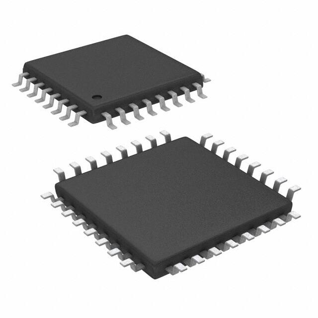
BODY SIZE (NOM)
5.00 mm × 5.00 mm
(1) For all available packages, see the package option addendum
at the end of the data sheet.
ADS127L01 Block Diagram
REFP
PACKAGE
TQFP (32)
-60
-80
-100
-120
FILTER [1:0]
CLK
ADS127L01
AGND
DGND
Copyright © 2016, Texas Instruments Incorporated
-140
-160
-180
0
20
40
60
80
Frequency (kHz)
100
120
1
An IMPORTANT NOTICE at the end of this data sheet addresses availability, warranty, changes, use in safety-critical applications,
intellectual property matters and other important disclaimers. PRODUCTION DATA.
�ADS127L01
SBAS607B – APRIL 2016 – REVISED SEPTEMBER 2016
www.ti.com
Table of Contents
1
2
3
4
5
6
Features ..................................................................
Applications ...........................................................
Description .............................................................
Revision History.....................................................
Pin Configuration and Functions .........................
Specifications.........................................................
1
1
1
2
4
6
6.1
6.2
6.3
6.4
6.5
6.6
6.7
6.8
6.9
Absolute Maximum Ratings ...................................... 6
ESD Ratings.............................................................. 6
Recommended Operating Conditions....................... 7
Thermal Information .................................................. 7
Electrical Characteristics........................................... 8
Timing Requirements: Serial Interface.................... 11
Switching Characteristics: Serial Interface Mode.... 11
Timing Requirements: Frame-Sync Master Mode .. 13
Switching Characteristics: Frame-Sync Master
Mode ........................................................................ 13
6.10 Timing Requirements: Frame-Sync Slave Mode .. 14
6.11 Switching Characteristics: Frame-Sync Slave
Mode ........................................................................ 14
6.12 Typical Characteristics .......................................... 16
7
Parameter Measurement information ................ 24
7.1 Noise Performance ................................................. 24
8
Detailed Description ............................................ 26
8.1 Overview ................................................................. 26
8.2 Functional Block Diagram ....................................... 26
8.3
8.4
8.5
8.6
9
Feature Description.................................................
Device Functional Modes........................................
Programming ..........................................................
Register Maps .........................................................
27
38
46
53
Application and Implementation ........................ 58
9.1
9.2
9.3
9.4
Application Information............................................
Typical Application .................................................
Do's and Don'ts ......................................................
Initialization Setup ..................................................
58
72
75
77
10 Power Supply Recommendations ..................... 78
10.1 Power-Supply Sequencing.................................... 78
10.2 Power-Supply Decoupling .................................... 78
11 Layout................................................................... 79
11.1 Layout Guidelines ................................................. 79
11.2 Layout Example .................................................... 80
12 Device and Documentation Support ................. 82
12.1
12.2
12.3
12.4
12.5
12.6
Documentation Support .......................................
Receiving Notification of Documentation Updates
Community Resources..........................................
Trademarks ...........................................................
Electrostatic Discharge Caution ............................
Glossary ................................................................
82
82
82
82
82
82
13 Mechanical, Packaging, and Orderable
Information ........................................................... 82
4 Revision History
Changes from Revision A (May 2016) to Revision B
Page
•
Features, Changed AC Performance To: AC + DC Performance.......................................................................................... 1
•
Features, Changed SNR: Up to 115.5 dB (at OSR 256 To: SNR: Up to 115.5 dB ............................................................... 1
•
Features, Changed THD: –126 dB 9LP and VLP modes) To: THD: Down to -129 dB.......................................................... 1
•
Features, Changed DC Accuracy To: Integral Nonlinearity: 1 ppm ...................................................................................... 1
•
Features, Changed HR: 111 dB SNR To: High-resolution ..................................................................................................... 1
•
Features, Changed LP: 108 dB SNR To: Low-power ............................................................................................................ 1
•
Features, Changed VLP: 105 dB SNR To: Very-low Power .................................................................................................. 1
•
Pin Functions, Changed pin 14 description of 1: Master mode.............................................................................................. 5
•
Pin Functions, Changed pin 19 description "protocol" To: interface ...................................................................................... 5
•
Pin Functions, Changed pin 27 description "Decouple DVDD to DGND with a 1-μF capacitor" To: Connect a 1-μF
capacitor to DGND ................................................................................................................................................................. 5
•
Pin Functions, Changed pin 32 description "Decouple AVDD to AGND with a 1-μF capacitor" To: Connect a 1-μF
capacitor to AGND.................................................................................................................................................................. 5
•
Recommended Operating Conditions, Changed VCM NOM value From: (AVDD + AGND) / 2 To: AVDD / 2 ...................... 7
•
Electrical Characteristics, Added test conditions to SNR: WB2, OSR 32/64/128, VREF = 3 V ............................................... 9
•
Figure 2, Changed th(DO) To: tv(DO) in order to match Switching Characteristics: Serial Interface Mode table...................... 12
•
Timing Requirements: Frame-Sync Slave Mode, Deleted text from conditions statement "and DVDD = 1.7 V to 3.6 V"... 14
•
Typical Characteristics, Changed conditions statement....................................................................................................... 16
•
Table 1, Changed the values in the ENOB column.............................................................................................................. 25
•
Table 2, Changed the values in the ENOB column.............................................................................................................. 25
•
Changed text frame-sync mode To: frame-sync interface mode throughout the document ................................................ 26
2
Submit Documentation Feedback
Copyright © 2016, Texas Instruments Incorporated
Product Folder Links: ADS127L01
�ADS127L01
www.ti.com
SBAS607B – APRIL 2016 – REVISED SEPTEMBER 2016
Revision History (continued)
•
Changed text frame-sync protocol. To: frame-sync interface mode throughout the document ........................................... 26
•
Changed section Mode Selection To: Operating Modes (HR, LP, VLP).............................................................................. 38
•
Changed section Filter Selection Pins (FILTER) To: Digital-Filter Path Selection Pins (FILTER[1:0]) ................................ 40
•
Figure 85, Changed tw(STH) To: tw(STL).................................................................................................................................... 41
•
Table 13, Changed tw(STH) To: tw(STL) ..................................................................................................................................... 41
•
Start Pin (START), Deleted text "For consistent performance, reassert START after device power-on when data first
appear, or after any hardware MODE pin change." ............................................................................................................. 42
•
Figure 86, Changed tw(STH) To: tw(STL).................................................................................................................................... 42
•
Table 14, Changed tw(STH) To: tw(STL) ..................................................................................................................................... 42
•
Data Ready (DRDY/FSYNC), Changed "...with the first SCLK rising edge." To: "...with the first SCLK falling edge, as
shown in Figure 91." ............................................................................................................................................................. 47
•
Data Ready (DRDY/FSYNC), Added text "A new conversion result is..."............................................................................ 47
•
Data Ready (DRDY/FSYNC), Added Figure 91 ................................................................................................................... 47
•
START (0000 100x), Added sentence "The START command is decoded..." ................................................................... 48
•
STOP (0000 101x) , Added sentence "The START pin must be held low..."....................................................................... 48
•
RREG (0010 rrrr 0000 nnnn), Added Figure 92 ................................................................................................................... 49
•
WREG (0100 rrrr 0000 nnnn), Added Figure 93 .................................................................................................................. 49
•
Synchronizing Devices, Added text "When synchronizing multiple devices..." .................................................................... 63
•
Figure 112, Changed position of fMOD arrow......................................................................................................................... 64
•
Antialiasing Filter, Changed paragraph following Figure 112 .............................................................................................. 65
•
Table 30, Changed THS4551 Gain Bandwidth Product (MHz) From: 130 To: 135 ............................................................. 66
•
Modulator Saturation, Added new section............................................................................................................................ 68
•
Table 32, Changed values in the Noise column................................................................................................................... 70
•
Detailed Design Procedure, Changed "With a 130-MHz gain-bandwidth product" To: "With a 135-MHz gainbandwidth product" .............................................................................................................................................................. 72
•
Layout Guidelines, Changed section.................................................................................................................................... 79
Changes from Original (April 2016) to Revision A
•
Page
Changed from product preview to production data ................................................................................................................ 1
Submit Documentation Feedback
Copyright © 2016, Texas Instruments Incorporated
Product Folder Links: ADS127L01
3
�ADS127L01
SBAS607B – APRIL 2016 – REVISED SEPTEMBER 2016
www.ti.com
5 Pin Configuration and Functions
AVDD
AGND
FORMAT
HR
RESET/PWDN
DVDD
DGND
CAP3
32
31
30
29
28
27
26
25
PBS package
32-Pin TQFP
Top View
AINN
3
22
SCLK
AINP
4
21
DIN
AGND
5
20
DOUT
AVDD
6
19
DRDY/FSYNC
REXT
7
18
DAISYIN
INTLDO
8
17
START
Not to scale
OSR0
OSR1
FILTER0
FSMODE
CAP2
FILTER1
REFN
REFP
16
CS
15
23
14
2
13
CAP1
12
CLK
11
24
10
1
9
LVDD
Pin Functions
PIN
DESCRIPTION (1)
I/O
NO.
NAME
1
LVDD
Supply
2
CAP1
Analog output
Modulator common-mode voltage.
Connect a 1-µF capacitor to AGND
3
AINN
Analog input
Negative analog input.
4
AINP
Analog input
Positive analog input.
5
AGND
Supply
Analog ground.
6
AVDD
Supply
Analog supply.
Connect a 1-μF capacitor to AGND.
7
REXT
Analog input
Analog power-scaling bias resistor pin.
Recommended external resistor values:
REXT = 60.4 kΩ to AGND for high-resolution (HR) and low-power (LP) modes
REXT = 120 kΩ to AGND for very-low-power (VLP) mode
8
INTLDO
Digital input
LVDD voltage selection pin (pull high to AVDD or low to AGND through 10-kΩ resistor).
0: Internal analog low-dropout regulator (LDO) for LVDD voltage supply.
1: External LVDD voltage supply.
9
REFP
Analog input
Positive analog reference input.
Connect a minimum 10-μF capacitor to REFN
10
REFN
Analog input
Negative analog reference input.
11
CAP2
Analog output
Reference common-mode voltage.
Connect a 1-µF capacitor to AGND.
(1)
4
LVDD analog supply.
INTLDO = 0: LVDD is an analog-supply output pin. Connect a 1-µF capacitor to AGND.
INTLDO = 1: LVDD is an analog-supply input pin. Connect to a 1.8-V supply.
See the Unused Inputs and Outputs section for unused pin connections.
Submit Documentation Feedback
Copyright © 2016, Texas Instruments Incorporated
Product Folder Links: ADS127L01
�ADS127L01
www.ti.com
SBAS607B – APRIL 2016 – REVISED SEPTEMBER 2016
Pin Functions (continued)
PIN
NO.
NAME
DESCRIPTION (1)
I/O
12
FILTER1
Digital input
13
FILTER0
Digital input
Digital filter select pin (2).
00: Wideband 1 filter (WB1)
01: Wideband 2 filter (WB2)
10: Low-latency filter (LL)
11: Reserved
14
FSMODE
Digital input
Frame-sync mode pin (2).
0: Slave mode
1: Master mode. Applies to Frame-Sync interface mode only. No effect in SPI interface
mode.
15
OSR1
Digital input
Oversampling ratio (OSR) pin for the decimation filters (2).
Wideband filters, FILTER[1:0] = 00 or 01:
00: 32x oversampling (OSR 32)
01: 64x oversampling (OSR 64)
10: 128x oversampling (OSR 128)
11: 256x oversampling (OSR 256)
16
OSR0
Digital input
17
START
Digital input
Synchronization signal to start or restart a conversion.
18
DAISYIN
Digital input
Daisy-chain input.
19
DRDY/FSYNC
Digital input/output
20
DOUT
Digital output
21
DIN
Digital input
22
SCLK
23
CS
Digital input
Chip select.
Tie directly to DGND when using the frame-sync interface.
24
CLK
Digital input
Master clock input.
25
CAP3
Analog output
26
DGND
Supply
Digital ground.
27
DVDD
Supply
Digital supply.
Connect a 1-μF capacitor to DGND (3)
28
RESET/PWDN
Digital input
Reset or power-down pin, active low (3).
Low-latency filter, FILTER[1:0] = 10:
00: 32x oversampling (OSR 32)
01: 128x oversampling (OSR 128)
10: 512x oversampling (OSR 512)
11: 2048x oversampling (OSR 2048)
SPI interface: Data ready, active low (3).
Frame-sync interface: Frame-sync input signal (3)
Serial data output
Serial data input.
Tie directly to DGND when using the frame-sync interface.
Digital input/output Serial clock input (3).
Internally-generated digital operating voltage.
Connect a 1-µF capacitor to DGND.
29
HR
Digital input
ADC operating mode (2).
1: High-resolution (HR)
0: Low-power (LP) or very-low-power (VLP) (4)
30
FORMAT
Digital input
Interface select pin (2).
0: SPI
1: Frame-Sync
31
AGND
Supply
Analog ground.
32
AVDD
Supply
Analog supply.
Decouple AVDD to AGND with a 1-μF capacitor.
(2)
(3)
(4)
Pull the hardware mode pins high to DVDD or low to DGND through 100-kΩ resistors.
See the Reset and Power-Down Pin (RESET/PWDN) section for specific hardware design details if using power-down mode.
Entering LP mode or VLP mode is set by REXT resistor value.
Submit Documentation Feedback
Copyright © 2016, Texas Instruments Incorporated
Product Folder Links: ADS127L01
5
�ADS127L01
SBAS607B – APRIL 2016 – REVISED SEPTEMBER 2016
www.ti.com
6 Specifications
6.1 Absolute Maximum Ratings (1)
Voltage
Current
MIN
MAX
AVDD to AGND
–0.3
4.0
DVDD to DGND
–0.3
4.0
LVDD to AGND
–0.3
2.0
AGND to DGND
–0.3
0.3
REFP to AGND
–0.3
AVDD + 0.3
REFN to AGND
–0.3
AVDD + 0.3
Analog input
AGND – 0.3
AVDD + 0.3
Digital input
DGND – 0.3
DVDD + 0.3
–10
10
–40
125
Input, continuous, any pin except power supply pins
(2)
Operating ambient, TA
Temperature
Junction, TJ
(2)
–60
V
mA
150
Storage, Tstg
(1)
UNIT
°C
150
Stresses beyond those listed under Absolute Maximum Ratings may cause permanent damage to the device. These are stress ratings
only, which do not imply functional operation of the device at these or any other conditions beyond those indicated under Recommended
Operating Conditions. Exposure to absolute-maximum-rated conditions for extended periods may affect device reliability.
Input pins are diode-clamped to the power-supply rails. Limit the input current to 10 mA or less if the analog input voltage exceeds
AVDD + 0.3 V or is less than AGND – 0.3 V, or if the digital input voltage exceeds DVDD + 0.3 V or is less than DGND – 0.3 V.
6.2 ESD Ratings
VALUE
V(ESD)
(1)
(2)
6
Electrostatic discharge
Human-body model (HBM), per ANSI/ESDA/JEDEC JS-001
(1)
Charged-device model (CDM), per JEDEC specification JESD22-C101 (2)
±2000
±1000
UNIT
V
JEDEC document JEP155 states that 500-V HBM allows safe manufacturing with a standard ESD control process.
JEDEC document JEP157 states that 250-V CDM allows safe manufacturing with a standard ESD control process.
Submit Documentation Feedback
Copyright © 2016, Texas Instruments Incorporated
Product Folder Links: ADS127L01
�ADS127L01
www.ti.com
SBAS607B – APRIL 2016 – REVISED SEPTEMBER 2016
6.3 Recommended Operating Conditions
over operating ambient temperature range (unless otherwise noted)
MIN
NOM
MAX
UNIT
2.7
3.0
3.6
V
1.7
1.8
1.9
V
1.7
1.8
3.6
V
POWER SUPPLY
AVDD
Analog power supply
LVDD
Low voltage analog supply
DVDD
Digital supply
INTLDO = 1
ANALOG INPUTS
VIN
Differential input voltage
VIN = (VAINP – VAINN)
–VREF
VREF
V
VAINP,
VAINN
Absolute input voltage
AINP or AINN to AGND
AGND
AVDD
V
VCM
Common-mode input voltage
VCM = (VAINP + VAINN) / 2
AVDD / 2
V
VOLTAGE REFERENCE INPUTS
VREFN
Negative reference input
VREFP
Positive reference input
VREF
Reference input voltage
AGND – 0.1
AGND
AGND + 1.0
V
VREFN + 0.5
2.5
AVDD
V
VREF = VREFP – VREFN
0.5
2.5
3.0
V
HR mode
0.1
16.384
17.6
LP mode
0.1
8.192
8.8
VLP mode
0.1
4.096
4.4
EXTERNAL CLOCK SOURCE
Master clock rate (1)
fCLK
MHz
DIGITAL INPUTS
Input voltage
DGND
DVDD
V
–40
125
°C
TEMPERATURE RANGE
TA
(1)
Operating ambient temperature
To meet maximum speed conditions, fCLK duty cycle must be 49% < duty cycle < 51%.
6.4 Thermal Information
ADS127L01
THERMAL METRIC (1)
PBS (TQFP)
UNIT
32 PINS
RθJA
Junction-to-ambient thermal resistance
73.4
°C/W
RθJC(top)
Junction-to-case (top) thermal resistance
15.9
°C/W
RθJB
Junction-to-board thermal resistance
26.7
°C/W
ψJT
Junction-to-top characterization parameter
0.4
°C/W
ψJB
Junction-to-board characterization parameter
26.5
°C/W
RθJC(bot)
Junction-to-case (bottom) thermal resistance
N/A
°C/W
(1)
For more information about traditional and new thermal metrics, see the Semiconductor and IC Package Thermal Metrics application
report.
Submit Documentation Feedback
Copyright © 2016, Texas Instruments Incorporated
Product Folder Links: ADS127L01
7
�ADS127L01
SBAS607B – APRIL 2016 – REVISED SEPTEMBER 2016
www.ti.com
6.5 Electrical Characteristics
Minimum and maximum specifications apply from TA = –40°C to +125°C. Typical specifications are at TA = 25°C.
All specifications are at AVDD = 3 V, LVDD = 1.8 V (external), DVDD = 1.8 V, VREF = 2.5 V, INTLDO = 1, FILTER[1:0] = 01
(WB2), and fCLK = 16.384 MHz for HR mode, 8.192 MHz for LP mode, or 4.096 MHz for VLP mode (unless otherwise noted)
PARAMETER
TEST CONDITIONS
MIN
TYP
MAX
UNIT
ANALOG INPUTS
HR mode, fCLK = 16.384 MHz
Differential input
impedance
5
LP mode, fCLK = 8.192 MHz
11
VLP mode, fCLK = 4.096 MHz
23
kΩ
DC PERFORMANCE
Resolution
No missing codes
HR mode
fDATA
Data rate
LP mode
VLP mode
Integral nonlinearity (1)
INL
24
Wideband filters
Bits
512, 256, 128, 64
Low-latency filter
512, 128, 32, 8
Wideband filters
256, 128, 64, 32
Low-latency filter
256, 64, 16, 4
Wideband filters
128, 64, 32, 16
Low-latency filter
128, 32, 8, 2
HR mode
VCM = AVDD / 2
2.5
10
LP mode
VCM = AVDD / 2
1
5
VLP mode
VCM = AVDD / 2
1
5
Offset error
±0.1
Offset drift
1.5
Gain error
Noise
(2)
%FSR
HR mode
0.8
3
LP mode
0.4
2.5
VLP mode
0.2
2
HR mode
CMRR
fCM = 60 Hz
PSRR
Power-supply rejection
ratio
fPS = 60 Hz
8
μV/°C
0.003%
Common-mode rejection
ratio
(1)
(2)
ppm
mV
3.0
0.2
Gain calibration accuracy
Gain drift
kSPS
WB2, OSR 32
10.6
WB2, OSR 64
7.3
10.1
WB2, OSR 128
5.1
7.2
WB2, OSR 256
3.6
5.2
95
AVDD
90
DVDD
85
LVDD
80
ppm/°C
μVRMS
dB
dB
Best fit method.
For all Wideband filter configurations, see Table 1. For all Low-latency filter configurations, see Table 2.
Submit Documentation Feedback
Copyright © 2016, Texas Instruments Incorporated
Product Folder Links: ADS127L01
�ADS127L01
www.ti.com
SBAS607B – APRIL 2016 – REVISED SEPTEMBER 2016
Electrical Characteristics (continued)
Minimum and maximum specifications apply from TA = –40°C to +125°C. Typical specifications are at TA = 25°C.
All specifications are at AVDD = 3 V, LVDD = 1.8 V (external), DVDD = 1.8 V, VREF = 2.5 V, INTLDO = 1, FILTER[1:0] = 01
(WB2), and fCLK = 16.384 MHz for HR mode, 8.192 MHz for LP mode, or 4.096 MHz for VLP mode (unless otherwise noted)
PARAMETER
TEST CONDITIONS
MIN
TYP
MAX
UNIT
AC PERFORMANCE
WB2, OSR 32
Signal-to-noise ratio (2) (3)
SNR
Total harmonic
distortion (4)
THD
SFDR
Spurious-free dynamic
range
104.4
WB2, OSR 64
104.9
107.8
WB2, OSR 128
107.9
110.9
WB2, OSR 256
110.6
113.9
WB2, OSR 32, VREF = 3 V
105.8
WB2, OSR 64, VREF = 3 V
109.3
WB2, OSR 128, VREF = 3 V
112
WB2, OSR 256, VREF = 3 V
115.5
HR mode, fIN = 4 kHz, VIN = –0.5 dBFS
–113
LP mode, fIN = 4 kHz, VIN = –0.5 dBFS
–126
VLP mode, fIN = 4 kHz, VIN = –0.5 dBFS
–129
HR mode
–115
LP mode
–130
VLP mode
–130
dB
dB
dB
DIGITAL FILTER RESPONSE: WIDEBAND
Bandwidth
See Table 1
Pass-band ripple
±0.000032
FILTER[1:0] = 00 (WB1)
(0.45 to 0.55) ×
fDATA
FILTER[1:0] = 01 (WB2)
(0.40 to 0.50) ×
fDATA
Transition band
Stop-band attenuation
Hz
116
Group delay
Settling time
dB
Complete settling
dB
42 / fDATA
s
84 / fDATA
s
DIGITAL FILTER RESPONSE: LOW-LATENCY
Bandwidth
See Table 2
Group delay
See Low-Latency Filter section
Settling time
See Low-Latency Filter section
VOLTAGE REFERENCE INPUTS
Reference input
impedance
HR mode
2.2
LP mode
3.2
VLP mode
kΩ
4
SYSTEM MONITORS
Input over-range detect
accuracy
±100
mV
DIGITAL INPUT/OUTPUT (DVDD = 1.7 V to 3.6 V)
VIH
High-level input voltage
0.7 DVDD
DVDD
V
VIL
Low-level input voltage
DGND
0.3 DVDD
V
VOH
High-level output voltage
IOH = 2 mA
0.8 DVDD
DVDD
V
VOL
Low-level output voltage
IOL = 2 mA
DGND
0.2 DVDD
V
IH
Input leakage, high
IH = 3.6 V
–10
10
μA
IL
Input leakage, low
IL = DGND
–10
10
μA
(3)
(4)
Minimum SNR is ensured by the limit of the dc noise specification.
THD includes the first nine harmonics of the input signal.
Submit Documentation Feedback
Copyright © 2016, Texas Instruments Incorporated
Product Folder Links: ADS127L01
9
�ADS127L01
SBAS607B – APRIL 2016 – REVISED SEPTEMBER 2016
www.ti.com
Electrical Characteristics (continued)
Minimum and maximum specifications apply from TA = –40°C to +125°C. Typical specifications are at TA = 25°C.
All specifications are at AVDD = 3 V, LVDD = 1.8 V (external), DVDD = 1.8 V, VREF = 2.5 V, INTLDO = 1, FILTER[1:0] = 01
(WB2), and fCLK = 16.384 MHz for HR mode, 8.192 MHz for LP mode, or 4.096 MHz for VLP mode (unless otherwise noted)
PARAMETER
TEST CONDITIONS
MIN
TYP
MAX
UNIT
POWER SUPPLY
INTLDO = 0
AVDD
Power-down current
IAVDD
ILVDD
IDVDD
PD
(5)
(6)
10
AVDD current
LVDD current (5)
(6)
DVDD current (2)
Power dissipation
INTLDO = 1
8
2
μA
DVDD
0.6
LVDD, INTLDO = 1
0.6
HR mode
1.3
1.6
LP mode
0.8
1.0
VLP mode
0.4
0.6
HR mode
9.3
11
LP mode
4.6
5.5
VLP mode
2.3
2.8
HR mode
OSR 128
2.8
3.4
LP mode
OSR 128
1.5
1.8
VLP mode
OSR 128
0.8
1.1
HR mode, OSR 128,
AVDD = 3.0 V,
DVDD = 1.8 V
INTLDO = 1,
LVDD = 1.8 V,
25.7
30.8
INTLDO = 0
36.8
44.2
LP mode, OSR 128,
AVDD = 3.0 V,
DVDD = 1.8 V
INTLDO = 1,
LVDD = 1.8 V,
13.4
16.1
INTLDO = 0
18.9
22.7
VLP mode, OSR 128,
AVDD = 3.0 V,
DVDD = 1.8 V
INTLDO = 1,
LVDD = 1.8 V,
6.8
8.2
INTLDO = 0
9.5
11.4
mA
mA
mA
mW
LVDD current sourced from AVDD when the internal LDO is used (INTLDO = 0).
LVDD current scales with fCLK; see Figure 47.
Submit Documentation Feedback
Copyright © 2016, Texas Instruments Incorporated
Product Folder Links: ADS127L01
�ADS127L01
www.ti.com
SBAS607B – APRIL 2016 – REVISED SEPTEMBER 2016
6.6 Timing Requirements: Serial Interface
over operating ambient temperature range (unless otherwise noted)
tc(CLK)
tw(CP)
2.8 V < DVDD ≤ 3.6 V
1.7 V ≤ DVDD ≤ 2.8 V
MIN
MAX
MIN
HR mode
57
10,000
57
10,000
LP mode
114
10,000
114
10,000
VLP mode
227
10,000
227
10,000
HR mode
Pulse duration, Master clock
LP mode
high or low
VLP mode
28
5,000
28
5,000
56
5,000
56
5,000
112
5,000
112
5,000
Master clock period
TYP
TYP
MAX
UNIT
ns
ns
td(CSSC)
Delay time, CS falling edge to first SCLK rising
edge (1)
tc(SC)
SCLK period
40
tw(SCHL)
Pulse duration, SCLK high or low
20
25
ns
tsu(DI)
Setup time, DIN valid before SCLK falling edge
6
9
ns
th(DI)
Hold time, DIN valid after SCLK falling edge
8
9
ns
tw(CSH)
Pulse duration, CS high
6
6
tCLK
td(SCCS)
Delay time, final SCLK falling edge to CS rising
edge
2
2
tCLK
td(DECODE)
Delay time, command decode time
4
SPI timeout (2)
12
6250
ns
50
6250
4
ns
tCLK
16
16
TOUT_DEL = 0
2
2
tCLK
TOUT_DEL = 1
214
214
tCLK
tsu(DCI)
Setup time, DAISYIN valid before SCLK falling
edge
th(DCI)
Hold time, DAISYIN valid after SCLK falling
edge
(1)
(2)
8
5
8
ns
20
25
ns
CS can be tied low permanently in case the serial bus is not shared with any other device.
See the SPI Timeout section for more information.
6.7 Switching Characteristics: Serial Interface Mode
over operating ambient temperature range (unless otherwise noted)
2.8 V < DVDD ≤ 3.6 V
1.7 V ≤ DVDD ≤ 2.8 V
MIN
MIN
TYP
MAX
TYP
MAX
UNIT
tp(CSDO)
Propagation delay time,
CS falling edge to DOUT driven
12
18
ns
tp(SCDO)
Propagation delay time,
SCLK rising edge to valid new DOUT
15
21
ns
tv(DO)
Valid time, SCLK falling edge to DOUT invalid
tp(CSDOZ)
Propagation delay time,
CS rising edge to DOUT high impedance
18
tSCLK / 2
20
20
tSCLK / 2
ns
20
Submit Documentation Feedback
Copyright © 2016, Texas Instruments Incorporated
Product Folder Links: ADS127L01
ns
11
�ADS127L01
SBAS607B – APRIL 2016 – REVISED SEPTEMBER 2016
www.ti.com
tw(CP)
tc(CLK)
CLK
tw(CSH)
td(DECODE)
CS
td(CSSC)
SCLK
1
tw(SCHL)
tc(SC)
2
3
8
1
2
3
th(DI)
tsu(DI)
td(SCCS)
8
tv(DO)
tp(SCDO)
DIN
tp(CSDOZ)
tp(CSDO)
DOUT
NOTE: SPI settings are CPOL = 0 and CPHA = 1.
Figure 1. SPI Interface Timing
DAISYIN
MSBD1
LSBD1
tsu(DCI)
th(DCI)
SCLK
tv(DO)
DOUT
MSBD0
LSBD0
MSBD1
Figure 2. SPI Daisy-Chain Interface Timing
12
Submit Documentation Feedback
Copyright © 2016, Texas Instruments Incorporated
Product Folder Links: ADS127L01
�ADS127L01
www.ti.com
SBAS607B – APRIL 2016 – REVISED SEPTEMBER 2016
6.8 Timing Requirements: Frame-Sync Master Mode
over operating ambient temperature range and DVDD = 1.7 V to 3.6 V (unless otherwise noted)
1.7 V ≤ DVDD ≤ 3.6 V
MIN
tc(CLK)
tw(CP)
Master clock period
Pulse duration, Master clock high or low
TYP
MAX
HR mode
57
10,000
LP mode
114
10,000
VLP mode
227
10,000
HR mode
28
5,000
LP mode
56
5,000
112
5,000
VLP mode
UNIT
ns
ns
6.9 Switching Characteristics: Frame-Sync Master Mode
over operating free-air temperature range (unless otherwise noted)
2.8 V < DVDD ≤ 3.6 V
1.7 V ≤ DVDD ≤ 2.8 V
MIN
MIN
TYP
MAX
TYP
MAX
UNIT
td(CSC)
Delay time, CLK rising edge to SCLK falling
edge
tc(FRAME)
Frame period
tw(FP)
Pulse duration, FSYNC high or low
td(FSSC)
Delay time, FSYNC rising edge to SCLK falling
edge
tc(SC)
SCLK period
1 / (32fDATA)
1 / (32fDATA)
s
tw(SCHL)
Pulse duration, SCLK high or low
1 / (64fDATA)
1 / (64fDATA)
s
tv(DO)
Valid time, SCLK rising edge to DOUT invalid
tp(SCDO)
Propagation delay time,
SCLK falling edge to DOUT driven
15
17
ns
tp(FSDO)
Propagation delay time,
FSYNC rising edge to DOUT MSB valid
12
15
ns
15
15
ns
1 / fDATA
1 / fDATA
s
1 / (2fDATA)
1 / (2fDATA)
s
6
25
8
25
ns
ns
tw(CP)
tc(CLK)
CLK
tc(FRAME)
td(CSC)
tw(FP)
FSYNC
td(FSSC)
tw(SCHL)
tc(SC)
SCLK
tp(FSDO)
tv(DO)
tp(SCDO)
DOUT
Bit 31
Bit 30
Bit 15
Bit 14
Bit 0
Figure 3. Frame-Sync Interface Timing Master Mode
Submit Documentation Feedback
Copyright © 2016, Texas Instruments Incorporated
Product Folder Links: ADS127L01
13
�ADS127L01
SBAS607B – APRIL 2016 – REVISED SEPTEMBER 2016
www.ti.com
6.10 Timing Requirements: Frame-Sync Slave Mode
over operating ambient temperature range (unless otherwise noted)
tc(CLK)
1.7 V ≤ DVDD ≤ 2.8 V
MIN
MAX
MIN
HR mode
57
10,000
57
10,000
LP mode
114
10,000
114
10,000
VLP mode
227
10,000
227
10,000
HR mode
Pulse duration, Master clock
LP mode
high or low
VLP mode
28
5,000
28
5,000
56
5,000
56
5,000
112
5,000
112
5,000
Master clock period
tw(CP)
2.8 V < DVDD ≤ 3.6 V
TYP
TYP
MAX
UNIT
ns
ns
td(CSC)
Delay time, CLK rising edge to SCLK falling
edge
tc(FRAME)
Frame period
tw(FP)
Pulse durration, FSYNC high or low
td(FSSC)
Delay time, FSYNC rising edge to SCLK falling
edge
6
6
ns
td(SCFS)
Delay time, SCLK falling edge to FSYNC rising
edge
2
2
ns
tc(SC)
SCLK period
40
56
ns
tw(SCHL)
Pulse duration, SCLK high or low
20
28
ns
8
8
ns
25
31
ns
2
2
1 / fDATA
ns
1 / fDATA
2
s
2
tSCLK
DAISY-CHAIN TIMING
tsu(DCI)
Setup time, DAISYIN valid before SCLK rising
edge
th(DCI)
Hold time, DAISYIN valid after SCLK rising
edge
6.11 Switching Characteristics: Frame-Sync Slave Mode
over operating ambient temperature range (unless otherwise noted)
tv(DO)
Valid time, SCLK rising edge to DOUT invalid
tp(SCDO)
Propagation delay time,
SCLK falling edge to valid new DOUT
tp(FSDO)
Propagation delay time,
FSYNC rising edge to DOUT MSB valid
2.8 V < DVDD ≤ 3.6 V
1.7 V ≤ DVDD ≤ 2.8 V
MIN
MIN
TYP
MAX
17
TYP
MAX
25
ns
22
15
UNIT
22
25
22
ns
32
ns
tw(CP)
tc(CLK)
CLK
td(CSC)
tc(FRAME)
FSYNC
tw(FP)
td(FSSC)
td(SCFS)
tw(SCHL)
tc(SC)
SCLK
tp(FSDO)
tv(DO)
tp(SCDO)
DOUT
Bit 31
Bit 30
Bit 15
Bit 14
Bit 0
Figure 4. Frame-Sync Interface Timing Slave Mode
14
Submit Documentation Feedback
Copyright © 2016, Texas Instruments Incorporated
Product Folder Links: ADS127L01
�ADS127L01
www.ti.com
SBAS607B – APRIL 2016 – REVISED SEPTEMBER 2016
MSBD1
DAISYIN
LSBD1
tsu(DCI)
th(DCI)
SCLK
DOUT
MSBD0
LSBD0
MSBD1
Figure 5. Frame-Sync Interface Slave Daisy-Chain Timing
Submit Documentation Feedback
Copyright © 2016, Texas Instruments Incorporated
Product Folder Links: ADS127L01
15
�ADS127L01
SBAS607B – APRIL 2016 – REVISED SEPTEMBER 2016
www.ti.com
6.12 Typical Characteristics
0
0
-20
-20
-40
-40
-60
-60
Amplitude (dB)
Amplitude (dB)
At TA = 25°C, AVDD = 3.3 V, and external VREF = 2.5 V (unless otherwise noted)
-80
-100
-120
-80
-100
-120
-140
-140
-160
-160
-180
-180
0
40
80
120
160
Frequency (kHz)
200
240
0
40
fIN = 4 kHz, VIN = –0.5 dBFS, HR mode, WB2, 512 kSPS,
32768 samples
0
-20
-20
-40
-40
-60
-60
Amplitude (dB)
Amplitude (dB)
200
240
D027
Figure 7. Output Spectrum
0
-80
-100
-120
-80
-100
-120
-140
-140
-160
-160
-180
-180
0
40
80
120
160
Frequency (kHz)
200
240
0
40
80
D028
fIN = 4 kHz, VIN = –0.5 dBFS, HR mode, WB1, 512 kSPS,
32768 samples
120
160
Frequency (kHz)
200
240
D029
fIN = 4 kHz, VIN = –20 dBFS, HR mode, WB1, 512 kSPS,
32768 samples
Figure 8. Output Spectrum
Figure 9. Output Spectrum
0
0
-20
-20
-40
-40
-60
-60
Amplitude (dB)
Amplitude (dB)
120
160
Frequency (kHz)
fIN = 4 kHz, VIN = –20 dBFS, HR mode, WB2, 512 kSPS,
32768 samples
Figure 6. Output Spectrum
-80
-100
-120
-80
-100
-120
-140
-140
-160
-160
-180
-180
0
20
40
60
80
Frequency (kHz)
100
120 130
0
D030
fIN = 4 kHz, VIN = –0.5 dBFS, LP mode, WB2, 256 kSPS,
32768 samples
20
40
60
80
Frequency (kHz)
100
120 130
D031
fIN = 4 kHz, VIN = –20 dBFS, LP mode, WB2, 256 kSPS,
32768 samples
Figure 10. Output Spectrum
16
80
D026
Figure 11. Output Spectrum
Submit Documentation Feedback
Copyright © 2016, Texas Instruments Incorporated
Product Folder Links: ADS127L01
�ADS127L01
www.ti.com
SBAS607B – APRIL 2016 – REVISED SEPTEMBER 2016
Typical Characteristics (continued)
0
0
-20
-20
-40
-40
-60
-60
Amplitude (dB)
Amplitude (dB)
At TA = 25°C, AVDD = 3.3 V, and external VREF = 2.5 V (unless otherwise noted)
-80
-100
-120
-80
-100
-120
-140
-140
-160
-160
-180
-180
0
10
20
30
40
Frequency (kHz)
50
60 65
0
5
D032
fIN = 4 kHz, VIN = –0.5 dBFS, VLP mode, WB2, 128 kSPS,
32768 samples
10 15 20 25 30 35 40 45 50 55 60 65
Frequency (kHz)
D033
fIN = 4 kHz, VIN = –20 dBFS, VLP mode, WB2, 128 kSPS,
32768 samples
Figure 13. Output Spectrum
0
-20
-20
-40
-40
-60
-60
Amplitude (dB)
Amplitude (dB)
Figure 12. Output Spectrum
0
-80
-100
-120
-80
-100
-120
-140
-140
-160
-160
-180
-180
0
30
60
90
120 150 180
Frequency (kHz)
210
0
240
20
40
D034
Inputs shorted, HR mode, WB2, 512 kSPS,
32768 samples
60
80
Frequency (kHz)
100
120
D035
Inputs shorted, LP mode, WB2, 256 kSPS,
32768 samples
Figure 14. Output Spectrum
Figure 15. Output Spectrum
0
30
25
-20
20
Output Voltage (PV)
Amplitude (dB)
-40
-60
-80
-100
-120
15
10
5
0
-5
-10
-15
-140
-20
-160
-25
-180
-30
0
5
10 15 20 25 30 35 40 45 50 55 60 65
Frequency (kHz)
D036
Inputs shorted, VLP mode, WB2, 128 kSPS,
32768 samples
0
12000
24000
36000
Time (Ps)
48000
60000
D039
HR mode, 0.5 seconds data collection
space
Figure 16. Output Spectrum
Figure 17. ADC Conversion Noise
Submit Documentation Feedback
Copyright © 2016, Texas Instruments Incorporated
Product Folder Links: ADS127L01
17
�ADS127L01
SBAS607B – APRIL 2016 – REVISED SEPTEMBER 2016
www.ti.com
Typical Characteristics (continued)
12
Voltage (PV)
10
8
6
4
2
0
-2
-4
-6
-8
-10
Noise (PVRMS)
4200
3900
3600
3300
3000
2700
2400
2100
1800
1500
1200
900
600
300
0
-12
Number of Occurrences
At TA = 25°C, AVDD = 3.3 V, and external VREF = 2.5 V (unless otherwise noted)
5.2
5.18
5.16
5.14
5.12
5.1
5.08
5.06
5.04
5.02
5
4.98
4.96
4.94
4.92
4.9
0.5
0.75
1
1.25
D040
9
5.15
8
5.125
Noise (PVRMS)
7
Noise (PVrms)
2.25
2.5
2.75
3
D053
Figure 19. Noise vs VREF
Figure 18. Noise Histogram
6
5
4
5.1
5.075
5.05
5.025
3
2
-40
5
-20
0
20
40
60
Temperature (qC)
80
100
120
0
2
D048
Inputs shorted
4
6
8
10
fCLK (MHz)
12
14
16
18
D055
Inputs shorted, HR mode
Figure 20. Noise vs Temperature
Figure 21. Noise vs fCLK
0
HR Mode
LP Mode
VLP Mode
-30
-45
-60
-75
-90
-105
Total Harmonic Distortion (dB)
0
-15
Total Harmonic Distortion (dB)
1.75 2
VREF (V)
Inputs shorted, HR mode
Inputs shorted, HR mode, 65536 points
HR Mode
LP Mode
VLP Mode
-20
-40
-60
-80
-100
-120
-140
-120
-135
0.5 0.7 1
2
3 4 5 6 7 8 10
20 30 4050 70 100
Input Frequency (kHz)
D037
-160
-60 -55 -50 -45 -40 -35 -30 -25 -20 -15 -10
Input Amplitude (dBFS)
WB2, OSR 32
-5
0
D038
WB2, OSR 32
Figure 22. Total Harmonic Distortion vs fIN
18
1.5
Figure 23. Total Harmonic Distortion vs VIN
Submit Documentation Feedback
Copyright © 2016, Texas Instruments Incorporated
Product Folder Links: ADS127L01
�ADS127L01
www.ti.com
SBAS607B – APRIL 2016 – REVISED SEPTEMBER 2016
Typical Characteristics (continued)
At TA = 25°C, AVDD = 3.3 V, and external VREF = 2.5 V (unless otherwise noted)
-100
-105
Total Harmonic Distortion (dB)
-110
-115
-120
-125
-105
-110
-115
-120
-125
-130
-135
-140
2.5
3
VREF (V)
0
2
4
HR mode, fIN = 4 kHz, VIN = –0.5 dBFS
5
2.5
-1
29
.8
04
.6
-1
08
.4
-1
-1
-1
16
.1
12
.3
0
20
16
18
D054
D074
HR mode, fIN = 4 kHz, VIN = –0.5 dBFS
Total Harmonic Distortion (dB)
.8
7.5
.2
10
-1
14
14
13
12
11
10
9
8
7
6
5
4
3
2
1
0
-1
28
Number of Occurrences
12.5
Number of Occurrences
12
Figure 25. Total Harmonic Distortion vs fCLK
15
Total Harmonic Distortion (dB)
8
10
fCLK (MHz)
fIN = 4 kHz, HR mode
Figure 24. Total Harmonic Distortion vs VREF
D072
LP mode, fIN = 4 kHz, VIN = –0.5 dBFS
Figure 26. Total Harmonic Distortion Histogram
Figure 27. Total Harmonic Distortion Histogram
10
8
9
7
8
HR Mode
LP Mode
VLP Mode
6
7
Linearity (ppm)
Number of Occurrences
6
D052
-1
21
2
.4
1.5
-1
23
1
25
-130
0.5
-1
Total Harmonic Distortion (dB)
-100
6
5
4
3
5
4
3
2
2
1
1
0
-40
Total Harmonic Distortion (dB)
22
.3
-1
24
.1
-1
-1
26
27
.9
-1
29
.7
-1
31
.6
-1
33
.5
-1
-1
35
.4
0
-20
D073
0
20
40
60
Temperature (qC)
80
100
120
D050
VLP mode, fIN = 4 kHz, VIN = –0.5 dBFS
Figure 28. Total Harmonic Distortion Histogram
Figure 29. INL vs Temperature
Submit Documentation Feedback
Copyright © 2016, Texas Instruments Incorporated
Product Folder Links: ADS127L01
19
�ADS127L01
SBAS607B – APRIL 2016 – REVISED SEPTEMBER 2016
www.ti.com
Typical Characteristics (continued)
At TA = 25°C, AVDD = 3.3 V, and external VREF = 2.5 V (unless otherwise noted)
3
2
1200
1.5
Number of Occurrences
1
0.5
0
-0.5
-1
-1.5
-2
1000
800
600
400
200
-2.5
D051
16
1
1
12
81
41
1
9
9
0
2.5
-3
2
-7
1.5
19
1
59
0
0.5
VIN (V)
-1
-0.5
-1
-1
99
-1.5
31
-2
-2
-3
-2.5
-1
Linearity Error (ppm)
1400
25qC
-40qC
125qC
2.5
Offset Error (PV)
D042
Inputs shorted
Figure 30. INL vs VIN
Figure 31. Offset Error Histogram
200
1400
150
100
1000
Offset Error (PV)
Number of Occurrences
1200
800
600
400
50
0
-50
-100
-150
-200
200
-250
-300
-40
53
-20
0
20
40
60
Temperature (qC)
1.
1.
2
87
0.
55
1
22
0.
0.
.1
3
-0
.4
6
-0
9
.7
.0
-0
1
-1
.4
-1
-1
.6
8
0
Gain Error (%FSR)
D041
80
100
120
D047
Inputs shorted
Figure 33. Offset Error vs Temperature
Figure 32. Gain Error Histogram
-0.24
10
9
Number of Occurrences
Gain Error (%FSR)
-0.21
-0.18
-0.15
-0.12
8
7
6
5
4
3
2
1
Offset Drift (PV/qC)
9
1.
79
68
1.
57
1.
47
1.
36
1.
1.
14
03
1.
1.
D049
92
0
120
0.
100
81
80
0.
20
40
60
Temperature (qC)
71
0
0.
-20
0.
6
-0.09
-40
D043
Inputs shorted, 30 devices
Figure 34. Gain Error vs Temperature
20
Submit Documentation Feedback
Figure 35. Offset Drift Histogram
Copyright © 2016, Texas Instruments Incorporated
Product Folder Links: ADS127L01
�ADS127L01
www.ti.com
SBAS607B – APRIL 2016 – REVISED SEPTEMBER 2016
Typical Characteristics (continued)
10
20
9
17.5
8
Number of Occurrences
Number of Occurrences
At TA = 25°C, AVDD = 3.3 V, and external VREF = 2.5 V (unless otherwise noted)
7
6
5
4
3
15
12.5
10
7.5
5
D045
LP mode, 30 Devices
Figure 36. Gain Drift Histogram
Figure 37. Gain Drift Histogram
0.22
20
TA = 25qC
TA = -40qC
TA = 125qC
0.21
18
0.2
16
Gain Error (%FSR)
0.19
14
12
10
8
6
0.18
0.17
0.16
0.15
0.14
0.13
4
0.12
2
0.11
0
0.1
0
-0
.4
-0
.1
4
0.
11
0.
36
0.
61
0.
87
1.
12
1.
37
1.
63
1.
88
2.
13
-0
.6
5
Number of Occurrences
53
Gain Drift (ppm/qC)
D044
HR mode, 30 Devices
Gain Error (ppm/qC)
1
2
3
4
5
6
D046
Figure 39. Gain Error vs fCLK
Figure 38. Gain Drift Histogram
250
5.29
TA = 25qC
TA = -40qC
TA = 125qC
200
5.27
Input Impedance (k:)
150
100
50
0
-50
-100
-150
5.25
5.23
5.21
5.19
5.17
5.15
-200
5.13
-250
5.11
-300
0
1
2
3
4
5
6
7 8 9 10 11 12 13 14 15 16 17
fCLK (MHz)
D061
HR mode
VLP mode, 30 Devices
Offset Error (PV)
1.
1.
25
97
0.
69
0.
3
0.
1
5
.1
-0
Gain Drift (ppm/qC)
-0
.4
3
74
2.
09
42
2.
76
2.
44
1.
1.
79
11
1.
0.
0.
0.
-0
.
-0
.
46
0
14
0
19
2.5
51
1
0.
41
2
7 8 9 10 11 12 13 14 15 16 17
fCLK (MHz)
D062
5.09
-40
-20
0
20
40
60
80
Temperature (qC)
100
120
140
D075
HR mode, fCLK = 16.384 MHz
Inputs shorted, HR mode
Figure 40. Offset Voltage vs fCLK
Figure 41. Differential Input Impedance vs Temperature
Submit Documentation Feedback
Copyright © 2016, Texas Instruments Incorporated
Product Folder Links: ADS127L01
21
�ADS127L01
SBAS607B – APRIL 2016 – REVISED SEPTEMBER 2016
www.ti.com
Typical Characteristics (continued)
At TA = 25°C, AVDD = 3.3 V, and external VREF = 2.5 V (unless otherwise noted)
180
180
AVDD
LVDD
DVDD
170
AVDD
DVDD
170
160
150
150
140
140
PSRR (dB)
PSRR (dB)
160
130
120
110
130
120
110
100
100
90
90
80
80
70
70
60
60
0
50
100
150
200 250 300
fPS (kHz)
350
400
450
500
0
50
100
HR mode, INTLDO = 1
Figure 42. PSRR vs Power-Supply Frequency
350
400
450
500
D077
Figure 43. PSRR vs Power-Supply Frequency
10
HR Mode
LP Mode
VLP Mode
HR Mode
LP Mode
VLP Mode
8
ILVDD (mA)
1.6
IAVDD (mA)
200 250 300
fPS (kHz)
HR mode, INTLDO = 0
2
1.2
0.8
0.4
0
-40
150
D076
6
4
2
-20
0
20
40
60
Temperature (qC)
80
100
0
-40
120
-20
0
20
40
60
Temperature (qC)
D056
Figure 44. IAVDD vs Temperature
80
100
120
D057
Figure 45. ILVDD vs Temperature
10
3
9
HR Mode
LP Mode
VLP Mode
8
7
ILVDD (mA)
IDVDD (mA)
2.4
1.8
1.2
6
5
4
3
0.6
HR Mode
LP Mode
VLP Mode
2
0
-40
1
-20
0
20
40
60
Temperature (qC)
80
100
0
120
1
2
D058
Figure 46. IDVDD vs Temperature
22
Submit Documentation Feedback
3
4
5
6
7 8 9 10 11 12 13 14 15 16 17
fCLK (MHz)
D063
Figure 47. ILVDD vs fCLK
Copyright © 2016, Texas Instruments Incorporated
Product Folder Links: ADS127L01
�ADS127L01
www.ti.com
SBAS607B – APRIL 2016 – REVISED SEPTEMBER 2016
Typical Characteristics (continued)
30
40
25
32
Power Dissipation (mW)
Power Dissipation (mW)
At TA = 25°C, AVDD = 3.3 V, and external VREF = 2.5 V (unless otherwise noted)
HR Mode
LP Mode
VLP Mode
20
15
10
HR Mode
LP Mode
VLP Mode
24
16
8
5
-40
-20
0
20
40
60
Temperature (qC)
80
100
0
-40
120
-20
0
D059
20
40
60
Temperature (qC)
INTLDO = 1, LVDD = 1.8 V
120
D060
Figure 49. Power Dissipation vs Temperature
0
0
-20
-20
-40
-40
-60
-60
Amplitude (dB)
Amplitude (dB)
100
INTLDO = 0
Figure 48. Power Dissipation vs Temperature
-80
-100
-120
-80
-100
-120
-140
-140
-160
-160
-180
-180
0
40
80
120
160
Frequency (kHz)
200
240
0
5
D064
Inputs shorted, HR mode, LL, 512 kSPS, 32768 samples
10 15 20 25 30 35 40 45 50 55 60 65
Frequency (kHz)
D065
Inputs shorted, HR mode, LL, 128 kSPS, 32768 samples
Figure 50. Output Spectrum
Figure 51. Output Spectrum
0
0
-20
-20
-40
-40
-60
-60
Amplitude (dB)
Amplitude (dB)
80
-80
-100
-120
-140
-80
-100
-120
-140
-160
-160
-180
-180
0
5
10 15 20 25 30 35 40 45 50 55 60 65
Frequency (kHz)
D065
Inputs shorted, HR mode, LL, 32 kSPS, 32768 samples
0
0.4
0.8
1.2
1.6
2
2.4
Frequency (kHz)
2.8
3.2
3.6
4
D067
Inputs shorted, HR mode, LL, 8 kSPS, 32768 samples
Figure 52. Output Spectrum
Figure 53. Output Spectrum
Submit Documentation Feedback
Copyright © 2016, Texas Instruments Incorporated
Product Folder Links: ADS127L01
23
�ADS127L01
SBAS607B – APRIL 2016 – REVISED SEPTEMBER 2016
www.ti.com
Typical Characteristics (continued)
5000
Number of Occurrences
4500
4000
3500
3000
2500
2000
1500
1000
500
8.
5
10
.2
4
2
6.
4.
2.
1
0
.1
-2
.2
.4
Figure 55. Noise Histogram
4.
1
3.
1
2
1
0
-1
Voltage (PV)
D070
Inputs shorted, HR mode, LL, 32 kSPS, 32768 samples
-2
-3
-3
.1
6500
6000
5500
5000
4500
4000
3500
3000
2500
2000
1500
1000
500
0
.9
6
Number of Occurrences
Noise (PV)
7.
6
4
2
0
-2
-4
-6
.6
D069
Inputs shorted, HR mode, LL, 128 kSPS, 32768 samples
Figure 54. Noise Histogram
7000
6500
6000
5500
5000
4500
4000
3500
3000
2500
2000
1500
1000
500
0
-7
-4
.5
Voltage (PV)
D068
Inputs shorted, HR mode, LL, 512 kSPS, 32768 samples
Number of Occurrences
-6
0.
2
-1
Voltage (PV)
-8
.5
.2
20
16
4
.8
10
5.
0
.4
-5
-1
0.
8
0
6.
2
-2
0.
5
7000
6500
6000
5500
5000
4500
4000
3500
3000
2500
2000
1500
1000
500
0
-1
Number of Occurrences
At TA = 25°C, AVDD = 3.3 V, and external VREF = 2.5 V (unless otherwise noted)
D071
Inputs shorted, HR mode, LL, 8 kSPS, 32768 samples
Figure 56. Noise Histogram
Figure 57. Noise Histogram
7 Parameter Measurement information
7.1 Noise Performance
Adjust the oversampling ratio (OSR) to control the data rate and change the digital filter in order to optimize the
noise performance of the ADS127L01. Hardware control pins offer four oversampling options and three
selectable digital filter options to configure the ADC for a specific bandwidth of interest. When averaging is
increased by reducing the data rate (increasing the OSR), the in-band noise drops as more samples from the
modulator are averaged to yield one conversion result. Table 1 and Table 2 summarize the device noise
performance across the various oversampling and digital filter options. Wideband 1 filter has a filter transition
band of (0.45 to 0.55) fDATA, and Wideband 2 filter has a filter transition band of (0.40 to 0.50) fDATA. Data are
representative of typical noise performance at TA = 25°C with an external 2.5-V reference. Data shown are the
result of one standard deviation of the readings with the inputs shorted together and biased to midsupply. A
minimum of 1,000 consecutive readings are used to calculate the VRMS_noise voltage noise for each
measurement. Equation 1 is used to convert the noise in VRMS_noise to SNR, and Equation 2 is used to convert
the noise in VRMS_noise to ENOB. The peak-to-peak noise for the Low-latency filter is defined as VPP_noise.
SNR = 20 × log (VREF × 0.7071 / VRMS_noise)
ENOB = In (2 x VREF / VRMS_noise) / In (2)
24
Submit Documentation Feedback
(1)
(2)
Copyright © 2016, Texas Instruments Incorporated
Product Folder Links: ADS127L01
�ADS127L01
www.ti.com
SBAS607B – APRIL 2016 – REVISED SEPTEMBER 2016
Noise Performance (continued)
Table 1. Wideband Filters Performance Summary
at AVDD = 3.0 V, DVDD = 1.8 V, and 2.5-V Reference
MODE
DATA RATE
(SPS)
OSR
512,000
32
256,000
64
128,000
128
64,000
256
256,000
32
128,000
64
64,000
128
32,000
256
128,000
32
64,000
64
32,000
128
16,000
256
High-resolution
(HR)
Low-power
(LP)
Very-low-power
(VLP)
TRANSITION BAND
PASS BAND
(kHz)
SNR
(dB)
VRMS_noise
(μVRMS)
ENOB
Wideband 1 filter
230.4
103.7
11.61
18.72
Wideband 2 filter
204.8
104.1
10.64
18.84
Wideband 1 filter
115.2
107.3
7.61
19.33
Wideband 2 filter
102.4
107.7
7.25
19.40
Wideband 1 filter
57.6
110.4
5.35
19.83
Wideband 2 filter
51.2
110.9
5.06
19.91
Wideband 1 filter
28.8
113.4
3.79
20.33
Wideband 2 filter
25.6
113.9
3.58
20.41
Wideband 1 filter
115.2
103.9
11.27
18.76
Wideband 2 filter
102.4
104.7
10.31
18.89
Wideband 1 filter
57.6
107.6
7.38
19.37
Wideband 2 filter
51.2
108.1
6.96
19.45
Wideband 1 filter
28.8
110.7
5.18
19.88
Wideband 2 filter
25.6
111.1
4.95
19.95
Wideband 1 filter
14.4
113.7
3.67
20.38
Wideband 2 filter
12.8
114.1
3.47
20.46
Wideband 1 filter
57.6
104.1
11.01
18.79
Wideband 2 filter
51.2
104.9
10.11
18.92
Wideband 1 filter
28.8
107.8
7.20
19.41
Wideband 2 filter
25.6
108.3
6.80
19.49
Wideband 1 filter
14.4
110.9
5.07
19.91
Wideband 2 filter
12.8
111.3
4.81
19.99
Wideband 1 filter
7.2
113.9
3.59
20.41
Wideband 2 filter
6.9
114.3
3.41
20.48
IDVDD
(mA)
7.50
4.35
2.80
2.00
3.80
2.25
1.50
1.10
1.95
1.20
0.80
0.60
Table 2. Low-Latency Filter Performance Summary
at AVDD = 3.0 V, DVDD = 1.8 V, and 2.5-V Reference
MODE
High-resolution
(HR)
Low-power
(LP)
Very-low-power
(VLP)
OSR
-3-dB
BANDWIDTH
(kHz)
SNR
(dB)
VRMS_noise
(μVRMS)
ENOB
VPP_noise
(μVPP)
IDVDD
(mA)
512,000
32
101.8
107.6
7.40
19.37
64.67
1.60
128,000
128
50.6
110.8
5.12
19.90
44.11
1.39
32,000
512
13.7
116.2
2.74
20.80
24.14
1.33
8,000
2048
3.5
122.0
1.41
21.76
11.32
1.32
256,000
32
50.9
107.8
7.22
19.40
61.99
0.85
64,000
128
25.3
111.0
4.97
19.94
46.79
0.75
16,000
512
6.9
116.5
2.65
20.85
22.05
0.73
4,000
2048
1.7
122.2
1.37
21.80
10.73
0.72
128,000
32
25.5
108.1
6.97
19.45
65.57
0.50
32,000
128
12.7
111.3
4.80
19.99
39.64
0.44
8,000
512
3.4
116.7
2.57
20.89
20.27
0.41
2,000
2048
0.9
122.4
1.34
21.83
10.73
0.40
DATA RATE
(SPS)
Submit Documentation Feedback
Copyright © 2016, Texas Instruments Incorporated
Product Folder Links: ADS127L01
25
�ADS127L01
SBAS607B – APRIL 2016 – REVISED SEPTEMBER 2016
www.ti.com
8 Detailed Description
8.1 Overview
The ADS127L01 is a 24-bit delta-sigma (ΔΣ) ADC that offers a combination of excellent dc accuracy and ac
performance. The flexible digital-filter options make it suitable for both dc and ac applications. The device is
hardware programmable, making it easy to configure for a variety of applications without the need to program
any registers.
The Functional Block Diagram shows the main internal features of the ADS127L01. The converter is comprised
of a third-order, chopper-stabilized, delta-sigma modulator, that measures the differential input signal, VIN =
(VAINP – VAINN), against the differential reference, VREF = (VREFP – VREFN). The converter core consists of a
differential, switched-capacitor, delta-sigma modulator followed by a selectable digital filter. The digital-filter lowlatency path uses a cascaded combination of a fifth-order sinc and a first-order sinc filter, ideal for applications
requiring fast response time or systems using a multiplexed input. Two wide-bandwidth paths (Wideband 1 and
Wideband 2) are also available, providing outstanding frequency response with very low pass-band ripple, a
steep-transition band, and high stop-band attenuation. The ADS127L01 provides two selectable options for
transition-band frequency. The Wideband-filter paths are suited for applications that require high-resolution
measurements of high-frequency, ac-signal content. To allow tradeoffs among speed, resolution, and power,
three operating modes are supported: high-resolution (HR), low-power (LP), and very-low-power (VLP).
In HR mode, SNR = 104.4 dB (VREF = 2.5 V) at a maximum data rate of 512 kSPS. At this data rate, the power
dissipation is only 35 mW, and scales with master clock frequency. In LP mode, the maximum data rate is 256
kSPS, while consuming only 19 mW of power. In VLP mode, the maximum data rate is 128 kSPS, while
consuming only 9 mW of power.
Configure the ADS127L01 by setting the appropriate hardware I/O pins. Registers are available for gain and
offset calibrations. Three interface communication modes are available, providing flexibility for convenient
interfacing to microcontrollers, DSPs, or FPGAs. SPI, frame-sync slave, or frame-sync master communication
modes are hardware selectable on the device. The ADS127L01 has a daisy-chain output available, and can
synchronize externally to another device or system using the START signal. The daisy-chain configuration allows
the device to be used conveniently in systems that require multiple channels.
8.2 Functional Block Diagram
REFP
REFN
LVDD AVDD
DVDD
LDO
INTLDO
SCLK
SPI and
Frame-Sync
Interface
Low-Latency
Filter
AINP
û ADC
Modulator
AINN
Wideband 1
Filter
CS
DIN
DOUT
DRDY/FSYNC
DAISYIN
Wideband 2
Filter
FSMODE
FORMAT
Control Logic
RESET/PWDN
OSR [1:0]
FILTER [1:0]
CLK
ADS127L01
DGND
AGND
Copyright © 2016, Texas Instruments Incorporated
26
Submit Documentation Feedback
Copyright © 2016, Texas Instruments Incorporated
Product Folder Links: ADS127L01
�ADS127L01
www.ti.com
SBAS607B – APRIL 2016 – REVISED SEPTEMBER 2016
8.3 Feature Description
This section discusses the details of the ADS127L01 internal functional elements. Throughout this document,
fCLK denotes the frequency of the signal at the CLK pin, tCLK denotes the period of the signal at the CLK pin, fDATA
denotes the output data rate, and tDATA denotes the time period of the output data.
8.3.1 Analog Inputs (AINP, AINN)
The ADS127L01 measures the differential input signal VIN = (VAINP – VAINN) against the differential reference
VREF = (VREFP – VREFN). The most positive measurable differential input is +VREF and the most negative
measurable differential input is –VREF.
For optimum performance, drive the ADS127L01 inputs differentially, centered around a common-mode voltage
of AVDD / 2. Alternatively, if the signal is of pseudo-differential nature, the negative input can be held at a
constant voltage other than 0 V (typically AVDD / 2), and the voltage on the positive input can change. Figure 58
and Figure 59 show examples of both fully-differential and pseudo-differential signals, respectively.
AINP
AINP
VCM
VCM
1.5 V
1.5 V
AINN
AINN
0V
0V
Figure 59. Pseudo-Differential Input Signal
Figure 58. Fully-Differential Input Signal
Electrostatic discharge (ESD) diodes to AVDD and AGND protect the inputs. To prevent the ESD diodes from
turning on, the absolute voltage on any input must stay within the range provided by Equation 3:
AGND – 0.3 V < VAINx < AVDD + 0.3 V
(3)
The analog input pins, AINP and AINN, at the front end of the converter are connected directly to the switchedcapacitor sampling network to measure the input voltage. Figure 60 shows a conceptual diagram of the
modulator circuit charging and discharging the sampling capacitor through switches, although the actual
implementation is slightly different. The sampling time (tCLK / 2) is equivalent to half the master clock period, and
is the inverse of the modulator sampling frequency.
AVDD AGND
tCLK = 1/fCLK
AINP
S1
S1
8 pF
S2
AINN
S1
ON
OFF
S2
ON
OFF
AVDD AGND
Copyright © 2016, Texas Instruments Incorporated
Figure 60. Equivalent Analog Input Circuitry
Submit Documentation Feedback
Copyright © 2016, Texas Instruments Incorporated
Product Folder Links: ADS127L01
27
�ADS127L01
SBAS607B – APRIL 2016 – REVISED SEPTEMBER 2016
www.ti.com
Feature Description (continued)
The average load presented by the switched-capacitor input can be modeled with an effective differential
impedance, as shown in Figure 61. The effective impedance is a function of the modulator clock, and is equal to
the master clock, fCLK. The ADS127L01 samples the input at very high speeds, and does not include an
integrated buffer; a suitable driver must be used. See the Application and Implementation section for
recommended driver circuit designs.
AINP
Zeff = 5 k
x (16.384 MHz/fCLK)
AINN
Figure 61. Effective Input Impedance
The ADC sampling network is connected to a delta-sigma modulator used to convert the analog input voltage
into a data bit stream. The modulator is third-order, with a multibit quantizer that runs at the modulator clock
frequency, fMOD, equal to the master clock frequency, fCLK.
8.3.2 Digital Filter
The ADS127L01 offers three selectable digital filters to perform both filtering and decimation of the digital data
stream coming from the modulator. The oversampling ratio (OSR) and digital-filter selection sets the overall
frequency response for the data converter. The available filter options for the ADS127L01 are:
• Low-latency sinc filter (LL)
• Wideband finite impulse response (FIR) filter with a transition band of (0.45 to 0.55) × fDATA (WB1)
• Wideband finite impulse response (FIR) filter with a transition band of (0.40 to 0.50) × fDATA (WB2)
Use the hardware FILTER[1:0] pins shown in Table 11. Each filter has four OSR options (the ratio of the
modulator sampling to the output data rate, or fMOD / fDATA), shown in Table 12, that are selectable through
hardware OSR[1:0] pins. The low-latency sinc filter is a cascaded sinc5 and sinc1 filter, and provides OSR
options to achieve data rates ranging from 8 kSPS to 512 kSPS when operating from a 16.384-MHz master
clock. The two Wideband filters use a multistage FIR topology to provide linear phase response with very low
pass-band ripple and high stop-band attenuation. Wideband filters 1 and 2 provide four OSRs to achieve data
rates ranging from 64 kSPS to 512 kSPS when operating from a 16.384-MHz master clock.
Select the filter and data rate when START is low, or take the START or RESET/PWDN pin low and back high
after a filter-path or data-rate change. If software commands are used to control conversions, use the STOP and
START commands after a change to the filter path selection or the data rate. If a conversion is in process during
a filter-path or data-rate change, the output data are not valid and must be discarded.
8.3.2.1 Low-Latency Filter
The low-latency sinc filter consists of two stages: a fixed-decimation, sinc5 filter, followed by a variabledecimation, sinc1 filter. The first-stage, sinc5 digital filter decimates by a fixed value of 32. When using OSR 32,
the first-stage digital filter bypasses the second filter stage, and has a sinc5 frequency response profile. The
second digital-filter stage provides an additional decimation of 4, 16, or 64 to create overall decimation options of
128, 512, and 2048. Together, the two stages create four selectable, Low-latency, filter data rates when operated
from a 16.384-MHz clock: 512 kSPS, 128 kSPS, 32 kSPS, and 4 kSPS.
8.3.2.1.1 Low-Latency Filter Frequency Response
The low-pass filtering effect of the sinc filter sets the overall frequency response of the ADC when in low-latency
filter mode. The frequency response of OSR 32 is from only the sinc5 filter stage. The frequency response of
OSR 128, 512, or 2048 is the product of the sinc5 first-stage and sinc1 second-stage frequency responses. The
overall filter response is given in Equation 4:
28
Submit Documentation Feedback
Copyright © 2016, Texas Instruments Incorporated
Product Folder Links: ADS127L01
�ADS127L01
www.ti.com
SBAS607B – APRIL 2016 – REVISED SEPTEMBER 2016
Feature Description (continued)
5
Hsinc 5 (f ) u Hsinc1 (f )
H(f )
ª 32Sf º
ª 32NSf º
sin «
sin «
»
»
fCLK ¼
¬ fCLK ¼
¬
u
ª Sf º
ª 32Sf º
32 u sin «
N u sin «
»
»
¬ fCLK ¼
¬ fCLK ¼
where
•
•
•
f = signal frequency
fCLK = ADC master clock frequency = ADC modulator clock frequency
N = Second-stage oversampling = 1 (OSR 32), 4 (OSR 128), 16 (OSR 512), or 64 (OSR 2048)
(4)
The inherent nature of the sinc filter response begins to attenuate frequencies as the signal moves away from dc.
The pass band droop for inband ac signals makes the low-latency filter less ideal for ac signals.
As shown in Figure 62 and Figure 63, when OSR is set to 32, the digital filter frequency response follows a sinc5
transfer function with nulls occurring at fDATA and at multiples thereof. At the null frequencies, the filter has zero
gain. Convert the x-axis from the data rate, fDATA, to terms of the master clock, fCLK, by using Equation 5:
fDATA = fCLK / OSR
(5)
0
0
-20
-25
-40
-50
-75
Amplitude (dB)
Amplitude (dB)
-60
-80
-100
-120
-100
-125
-150
-140
-175
-160
-200
-180
-225
-250
-200
0
0.5
1
1.5
2
2.5
3
3.5
4
Normalized Input Frequency (fIN/fDATA)
4.5
5
0
2
D001
Figure 62. Low-Latency Filter Frequency Response
(OSR 32)
4
6 8 10 12 14 16 18 20 22 24 26 28 30 32
Normalized Input Frequency (fIN/fDATA)
D002
Figure 63. Low-Latency Filter Frequency Response
(OSR 32) to fCLK
Adjust the digital-filter response by changing the OSR or the master clock, fCLK. Noise tradeoffs are made with
signal bandwidth and filter latency.
Selecting an OSR other than 32 superimposes new nulls from the second-stage sinc1 filter over the nulls
produced by the sinc5 stage. The end result is a combined frequency response from a sinc5 function at OSR 32
with nulls created from the sinc1 second stage at fDATA and multiple thereof.
Figure 64 and Figure 65 illustrate the normalized frequency response of the Low-latency filter across all four
OSR settings. OSR 32 follows a sinc5 frequency response, as highlighted in Figure 62. OSR 128, OSR 512, and
OSR 2048 show a combined sinc5 and sinc1 response.
Figure 66, Figure 67, and Figure 68 illustrate the frequency response of OSR 128, OSR 512, and OSR 2048,
respectively.
The Low-latency filter uses a multiple-stage, linear-phase, digital filter. Linear-phase filters exhibit constant delay
time versus input frequency (also known as constant group delay). This feature of linear phase filters means that
the time delay from any instant of the input signal to the corresponding same instant of the output data is
constant and independent of the input-signal frequency. This behavior results in essentially zero phase error
when measuring multitone signals.
Submit Documentation Feedback
Copyright © 2016, Texas Instruments Incorporated
Product Folder Links: ADS127L01
29
�ADS127L01
SBAS607B – APRIL 2016 – REVISED SEPTEMBER 2016
www.ti.com
0
0
-20
-2
-40
-4
-60
-6
Amplitude (dB)
Amplitude (dB)
Feature Description (continued)
-80
-100
-120
-140
-180
-10
-12
-14
OSR 32
OSR 128
OSR 512
OSR 2048
-160
-8
OSR 32
OSR 128
OSR 512
OSR 2048
-16
-18
-200
-20
0
0.5
1
1.5
2
2.5
3
3.5
4
Normalized Input Frequency (fIN/fDATA)
4.5
5
0
D003
Figure 64. Low-Latency Filter Frequency Response
0.5
D003
Figure 65. Low-Latency Filter Frequency Response
to 0.5 × fIN / fDATA
0
0
-25
-25
-50
-50
-75
Amplitude (dB)
-75
Amplitude (dB)
0.1
0.2
0.3
0.4
Normalized Input Frequency (fIN/fDATA)
-100
-125
-150
-100
-125
-150
-175
-175
-200
-200
-225
-225
-250
-250
0
20
40
60
80
100
Normalized Input Frequency (fIN/fDATA)
120
0
D004
Figure 66. Low-Latency Filter Frequency Response
(OSR 128) to fCLK
80
160
240
320
400
Normalized Input Frequency (fIN/fDATA)
480
D005
Figure 67. Low-Latency Filter Frequency Response
(OSR 512) to fCLK
0
-25
-50
Amplitude (dB)
-75
-100
-125
-150
-175
-200
-225
-250
0
300
600
900
1200
1500
1800
Normalized Input Frequency (fIN/fDATA)
2100
D006
Figure 68. Low-Latency Filter Frequency Response
(OSR 2048) to fCLK
30
Submit Documentation Feedback
Copyright © 2016, Texas Instruments Incorporated
Product Folder Links: ADS127L01
�ADS127L01
www.ti.com
SBAS607B – APRIL 2016 – REVISED SEPTEMBER 2016
Feature Description (continued)
8.3.2.1.2 Low-Latency Filter Settling Time
The Low-latency filter takes several conversion cycles to provide fully-settled data following a START pin low-tohigh transition or a START command. The OSR setting determines the exact number of conversion cycles for
first new available data, as shown in Table 3. In SPI mode, the DRDY signal remains high until settled data are
available. After settled data are available, a high-to-low transition on DRDY takes place. In frame-sync mode,
DOUT shifts zeroes until settled data are available. Figure 69 shows the relationship between START to the first
settled available data for SPI and frame-sync interface mode. See the Start Pin (START) section for exact timing
for the START pin to first available data.
START
Command
START
or
START Pin
DRDY
Settled Data
FSYNC
Figure 69. START to First Available Data
When applying an asynchronous step input to a converting ADS127L01, the output shift register does not gate
data during digital-filter settling. The step-input-setting timing diagram shown in Figure 70 illustrates the converter
step response with an asynchronous step input. The time that the analog input must be stable varies depending
on the OSR. Table 3 summarizes the settling time of the Low-latency filter when a step input is applied to the
input.
Step Input
DRDY
FSYNC
1
2
1
2
Figure 70. Asynchronous Step-Input Settling Time
Table 3. Low-Latency Filter Settling Time (Conversion Latency)
OSR
SETTLING TIME FROM START
(tCLK Periods)
INPUT SETTLING
(DRDY or FSYNC Pulses)
32
160
5
128
288
3
512
672
2
2048
2208
2
Submit Documentation Feedback
Copyright © 2016, Texas Instruments Incorporated
Product Folder Links: ADS127L01
31
�ADS127L01
SBAS607B – APRIL 2016 – REVISED SEPTEMBER 2016
www.ti.com
8.3.2.2 Wideband Filter
The two Wideband filters use a multistage FIR topology to provide linear phase response with minimal pass-band
ripple and high stop-band attenuation. The filters are well suited for measuring high-frequency ac signals while
still maintaining excellent dc accuracy. Both Wideband filter options offer the same four OSR options; 32, 64,
128, and 256. The difference is in the transition band. When these four OSRs are paired with a 16.384-MHz
clock, four selectable Wideband filter data rates are created: 512 kSPS, 256 kSPS, 128 kSPS, and 64 kSPS.
8.3.2.2.1 Wideband Filters Frequency Response
10
0
-10
-20
-30
-40
-50
-60
-70
-80
-90
-100
-110
-120
-130
-140
-150
Amplitude (dB)
Amplitude (dB)
Figure 71 shows the frequency response of the Wideband 1 filter with a transition band of (0.45 to 0.55) × fDATA
normalized to the output data rate, fDATA. Figure 72 shows the frequency response of the Wideband 2 filter with a
transition band of (0.40 to 0.50) × fDATA normalized to the output data rate, fDATA. These plots are valid for all of
the data rates available on the ADS127L01. Substitute the selected data rate, fDATA (calculated using
Equation 5), to express the x-axis in absolute frequency. Figure 73 overlaps the transition band of the Wideband
1 and Wideband 2 filters, showing the difference in frequency response. The Wideband 2 filter frequency
response is designed to attenuate out-of-band signals more than –116 dB by the Nyquist frequency (0.5 × fDATA)
to reduce the effects of aliasing near the transition band.
0
0.1
0.2 0.3 0.4 0.5 0.6 0.7 0.8
Normalized Input Frequency (fIN/fDATA)
0.9
1
10
0
-10
-20
-30
-40
-50
-60
-70
-80
-90
-100
-110
-120
-130
-140
-150
0
0.1
0.2 0.3 0.4 0.5 0.6 0.7 0.8
Normalized Input Frequency (fIN/fDATA)
D007
FILTER[1:0] = 00
Amplitude (dB)
1
D008
FILTER[1:0] = 01
Figure 71. Wideband 1 Filter Frequency Response
10
0
-10
-20
-30
-40
-50
-60
-70
-80
-90
-100
-110
-120
-130
-140
-150
0.35
0.9
Figure 72. Wideband 2 Filter Frequency Response
WB1 Filter
WB2 Filter
0.4
0.45
0.5
0.55
Normalized Input Frequency (fIN/fDATA)
0.6
D001
Figure 73. Wideband Filters Transition Band
32
Submit Documentation Feedback
Copyright © 2016, Texas Instruments Incorporated
Product Folder Links: ADS127L01
�ADS127L01
www.ti.com
SBAS607B – APRIL 2016 – REVISED SEPTEMBER 2016
0.00010
0.00010
0.00008
0.00008
0.00006
0.00006
0.00004
0.00004
Amplitude (dB)
Amplitude (dB)
The pass-band ripple for the two digital filters are shown in Figure 74 and Figure 75.
0.00002
0.00000
-0.00002
0.00002
0.00000
-0.00002
-0.00004
-0.00004
-0.00006
-0.00006
-0.00008
-0.00008
-0.00010
-0.00010
0
0.05 0.1 0.15 0.2 0.25 0.3 0.35 0.4 0.45 0.5 0.55
Normalized Input Frequency (fIN/fDATA)
D010
0
FILTER[1:0] = 00
0.05 0.1 0.15 0.2 0.25 0.3 0.35 0.4 0.45 0.5 0.55
Normalized Input Frequency (fIN/fDATA)
D011
FILTER[1:0] = 01
Figure 74. Pass Band Ripple for Wideband 1 Filter
Figure 75. Pass Band Ripple for Wideband 2 Filter
Amplitude (dB)
The overall frequency response repeats at the modulator sampling rate, which is the same as the input clock
frequency, fCLK. Figure 76 shows the response with the fastest data rate selected (512 kSPS when fCLK = 16.384
MHz).
10
0
-10
-20
-30
-40
-50
-60
-70
-80
-90
-100
-110
-120
-130
-140
-150
0
2
4
6 8 10 12 14 16 18 20 22 24 26 28 30 32
Normalized Input Frequency (fIN/fDATA)
D013
Figure 76. Extended Frequency Response of Wideband 1 Filter (OSR 32)
The Wideband filters use a multiple-stage, linear-phase, digital-filter architecture. Linear-phase filters exhibit
constant delay time versus input frequency (also known as constant group delay). This feature of linear phase
filters means that the time delay from any instant of the input signal to the corresponding same instant of the
output data is constant and independent of the input-signal frequency. This behavior results in essentially zero
phase error when measuring multitone signals.
Submit Documentation Feedback
Copyright © 2016, Texas Instruments Incorporated
Product Folder Links: ADS127L01
33
�ADS127L01
SBAS607B – APRIL 2016 – REVISED SEPTEMBER 2016
www.ti.com
8.3.2.2.2 Wideband Filters Settling Time
The Wideband filters fully settle before outputting data after the START pin low-to-high transition or a START
command is issued. The settling time of the Wideband filters is 84 conversion cycles; the DRDY signal idles high
and does not assert until new settled data are available in SPI interface mode. In frame-sync interface mode, the
output shift register outputs zeroes in place of the conversion data for 84 conversion cycles until the first settled
data are available. A step input on the analog input requires multiple conversions to settle if START is not
pulsed, or if the START command is not issued. Figure 77 shows the settling response with the x-axis
normalized to conversions or DRDY/FSYNC cycles.
150
Fully Settled Data at 84 Conversions
130
110
Settling (%)
90
70
50
30
10
-10
-30
-50
0
10
20
30
40
50
60
70
Conversions (1/fDATA)
80
90
100
D012
Figure 77. Step Response For Wideband Filters
60
120
65
115
70
110
75
105
80
100
Settling (%)
Settling (%)
Figure 78 and Figure 79 plot the undershoot and overshoot from the Wideband digital filter during an input step
function.
85
90
95
90
85
100
80
105
75
110
70
115
65
120
40
42
44
46
48
50
52
54
Conversions (1/fDATA)
56
58
60
60
40
42
D001
Figure 78. Wideband Filters Step-Response Undershoot
34
95
44
46
48
50
52
54
Conversions (1/fDATA)
56
58
60
D020
D001
Figure 79. Wideband Filters Step-Response Overshoot
Submit Documentation Feedback
Copyright © 2016, Texas Instruments Incorporated
Product Folder Links: ADS127L01
�ADS127L01
www.ti.com
SBAS607B – APRIL 2016 – REVISED SEPTEMBER 2016
8.3.3 Voltage Reference Inputs (REFP, REFN)
The ADC requires the connection of an external reference voltage for operation. The voltage reference for the
device is the differential voltage between REFP and REFN: VREF = (VREFP – VREFN). The reference inputs are not
buffered and use a sampling structure similar to that of the analog inputs, with the equivalent circuitry on the
reference inputs shown in Figure 80. The load across REFP and REFN is presented by the switched-capacitor in
parallel with a 6.4-kΩ resistor, and is modeled with an effective impedance (Zeff) proportional to the master clock,
fCLK, as shown in Figure 81.
REFP
REFN
AVDD
AVDD
AGND
AGND
Figure 80. Equivalent Reference Input Circuitry
REFP
Zeff = (3.4 k
REFN
× 16.384 MHz / fCLK) || 6.4 k
Figure 81. Effective Reference Impedance
ESD diodes protect the reference inputs. To keep these diodes from turning on, make sure the voltages on the
reference pins do not go below AGND by more than 0.3 V, and do not exceed AVDD by 0.3 V. Use external
Schottky clamp diodes or series resistors to limit the input current to safe values if the reference input may
exceed the absolute maximum ratings (see the Absolute Maximum Ratings table).
A high-quality reference voltage with the appropriate drive strength is required for achieving the best
performance from the ADS127L01. Noise and drift on the reference degrade overall system performance. Use a
minimum parallel combination of 10-µF and 0.1-µF ceramic bypass capacitors directly across the reference
inputs, REFP and REFN. Place these capacitors as close as possible to the device on the layout. See the
Application Information section for example reference circuits.
Submit Documentation Feedback
Copyright © 2016, Texas Instruments Incorporated
Product Folder Links: ADS127L01
35
�ADS127L01
SBAS607B – APRIL 2016 – REVISED SEPTEMBER 2016
www.ti.com
8.3.4 Clock Input (CLK)
The ADS127L01 requires an external clock for operation. This clock signal is used for the sampling network of
the modulator without any prescalers or dividers, and for the timing for the digital filter. Drive the ADC with an
external clock by applying the clock input to the CLK pin. At the maximum data rate, the clock input is 16.384
MHz for HR mode, 8.192 MHz for LP mode, and 4.096 MHz for VLP mode.
A high-quality, low-jitter clock is essential for optimum performance measuring the high-frequency input signals.
Any uncertainty during sampling of the input from clock jitter limits the maximum achievable SNR. For example,
uses an external clock with better than 10 psrms jitter for a 200-kHz fIN. For a lower fIN, the target jitter
requirement can be relaxed by –20 dB per decade. At fIN = 20 kHz, use a clock with better than 100-psrms jitter.
The selection of the external clock frequency (fCLK) does not affect the resolution of the ADS127L01. The output
data rates scale with fCLK frequency down to a minimum clock frequency of fCLK = 100 kHz. Use a slower fCLK to
reduce the ADC power consumption and relax the requirements of an external ADC drive circuit on the analog
input and reference input.
Crystal clock oscillators are the recommended clock source. Make sure to avoid excess ringing on the clock
input. A series resistor placed at the external clock buffer output often helps to reduce overshoot.
8.3.5 Out-of-Range-Detect System Monitor
An out-of-range-detect system-monitor bit (INP) is available in the status word (see the Status Word section).
The out-of-range detect bit flags (INP = 1) when the input exceeds the positive or negative full-scale range, set
by VREF, with each conversion result. The input is monitored using an analog comparator. The flag is issued
when the full-scale range is exceeded without waiting for the conversions to propagate through the digital filter.
The INP bit is used for narrow out-of-range input glitches that may or may not be removed by the ADC digital
filter.
8.3.6 System Calibration
The ADC incorporates optional offset- and gain-calibration registers to system-calibrate the ADC and signal chain
when in SPI interface mode. Enable the offset calibration register by setting FSC bit (bit 5 in the Configuration
register) to 1, and enable the gain calibration register by setting OFC bit (bit 4 in the Configuration register) to 1.
The programmable offset calibration value is 24 bits wide, and the gain calibration value is 16 bits wide. Use
calibration to correct internal ADC errors or overall system errors. Calibration is only supported through direct
user calibration, requiring the user to calculate and write the correction values to the calibration registers.
Perform a system offset calibration before full-scale calibration. After power-up, but before calibrating, wait for the
power supplies and reference voltage to fully settle.
As shown in Figure 82, the value of the offset calibration register is subtracted from the filter output, and then
multiplied by the full-scale register value. The data are then clipped to a 24-bit value to provide the final output.
AINP
AINN
Digital
Filter
ADC
+
Output Data
Clipped to 24 Bits
Final
Output
OFC[2:0] registers
(register addresses = 02h, 03h, 04h)
> 000000h: negative offset
000000h: no offset
< 000000h: positive offset
FSC[1:0] registers
(register addresses = 05h, 06h)
< 8000h: gain > 1
8000h: gain = 1
> 8000h: gain < 1
Figure 82. ADC Calibration Block Diagram
Equation 6 shows the internal calibration on the data result.
ADC Final Output Data = (Filter Output – OFC[23:0]) × FSC[15:0] / 8000h
36
Submit Documentation Feedback
(6)
Copyright © 2016, Texas Instruments Incorporated
Product Folder Links: ADS127L01
�ADS127L01
www.ti.com
SBAS607B – APRIL 2016 – REVISED SEPTEMBER 2016
The ADC offset calibration word is 24 bits, consisting of three 8-bit registers (OFC2, OFC, 1 OFC0), as shown in
Table 4. The offset value is twos complement format with a maximum positive value equal to 7FFFFFh (for
negative offset), and a maximum negative value equal to 800000h (for positive offset). A register value equal to
000000h has no offset correction. For offset calibration, short the ADC inputs or system inputs, and average the
conversions; averaging reduces noise for a more accurate calibration. Write the average value to the offset
calibration registers. The ADC subtracts the value from the conversion result.
Table 4. Offset Calibration Registers
REGISTER
BYTE
ORDER
ADDRESS
OFC0
LSB
02h
OFC_B7
OFC_B6
OFC_B5
OFC_B4
OFC_B3
OFC_B2
OFC_B1
OFC_B0
(LSB)
OFC1
MID
03h
OFC_B15
OFC_B14
OFC_B13
OFC_B12
OFC_B11
OFC_B10
OFC_B9
OFC_B8
OFC2
MSB
04h
OFC_B23
(MSB)
OFC_B22
OFC_B21
OFC_B20
OFC_B19
OFC_B18
OFC_B17
OFC_B16
BIT ORDER
The ADC gain calibration word is 16 bits consisting of two 8-bit registers (FSC1, FSC0), as shown in Table 5.
The full-scale calibration value is twos compliment, with a unity-gain correction factor at a register value equal to
8000h. Table 6 shows register values for selected gain factors.
Table 5. Gain Calibration Registers
REGISTER
BYTE
ORDER
ADDRESS
FSC0
LSB
05h
FSC_B7
FSC_B6
FSC_B5
FSC_B4
FSC_B3
FSC_B2
FSC_B1
FSC_B0
(LSB)
FSC1
MSB
06h
FSC_B15
(MSB)
FSC_B14
FSC_B13
FSC_B12
FSC_B11
FSC_B10
FSC_B9
FSC_B8
BIT ORDER
Table 6. Gain Calibration Register Values
FSCAL[2:0] REGISTER VALUE
GAIN FACTOR
7FFFh
2.00
8000h
1.00
0000h
0.00
For gain calibration, apply a dc calibration voltage that is less than positive full-scale voltage in order to avoid
clipped codes (VIN < +FSR), and average the conversions to reduce noise for a more accurate calibration. Gain
calibration is computed as shown in Equation 7, after offset error is removed.
Full-Scale Calibration = Expected Code Value / Actual Code Value
(7)
If the actual code is higher than the expected value, then the calculated calibration value is less than 8000h, and
the ADC gain is subsequently reduced. Write the calibration value to the gain calibration registers.
Submit Documentation Feedback
Copyright © 2016, Texas Instruments Incorporated
Product Folder Links: ADS127L01
37
�ADS127L01
SBAS607B – APRIL 2016 – REVISED SEPTEMBER 2016
www.ti.com
8.4 Device Functional Modes
8.4.1 Operating Modes (HR, LP, VLP)
The ADS127L01 offers three operational modes: high-resolution (HR), low-power (LP), and very-low-power
(VLP). These modes optimize power consumption by restricting the maximum master-clock frequency (fCLK)
controlling the data rate. The status of the HR pin determines if the device is in HR mode or LP mode. Enter VLP
mode by setting the ADS127L01 in LP mode, and increasing the value of the external REXT power scaling
resistor from 60.4 kΩ to 120 kΩ. The tolerance on the REXT power-scaling resistor must be 1% or better. The
analog current consumed by AVDD and LVDD decreases when in LP mode, and decreases further in VLP mode,
with a tighter restriction on maximum master-clock frequency. Table 7 details the HR pin and REXT settings for
each operating mode in the ADS127L01.
Table 7. Operating Mode Selection
OPERATING MODE
OPERATING MODE SELECTION PIN (HR)
REXT VALUE
MAXIMUM fCLK
High-Resolution (HR)
1
60.4 kΩ
17.6 MHz
Low-Power (LP)
0
60.4 kΩ
8.8 MHz
Very-Low-Power (VLP)
0
120 kΩ
4.4 MHz
8.4.2 Hardware Mode Pins
The ADS127L01 uses two-state hardware mode pins for ADC configuration. The operating mode, interface
selection, digital filter selection, and oversampling ratio (OSR) are all controlled through hardware pins. These
pins are constantly monitored, and set by either pulling them high to DVDD, or low to DGND. Use pull-up or pulldown 100-kΩ resistors, or directly tie the pins to microcontroller or DSP I/O lines to set the state of the pins.
When a change is sensed on the hardware mode pins after power-up, the ADC automatically issues a reset. To
ensure synchronization, issue a software reset command, or pulse the RESET/PWDN pin following the mode
change delay, td(MD).
When using the SPI interface mode, DRDY is held high after a mode change occurs until settled data are ready;
see Figure 83 and Table 8.
MODE
pin
td(MD)
ADS127L01
Mode
New Mode
Old Mode
td(FILT)
CLK
td(NDR)
DRDY
Figure 83. Mode Change Timing (SPI Interface)
Table 8. SPI Interface New Data After Mode Change
SYMBOL
38
DESCRIPTION
MIN
td(MD)
Delay time, MODE pin rising edge to mode change
td(FILT)
Delay time, mode change to first modulator sample
td(NDR)
Delay time for new data to be ready
TYP
3.5
MAX
UNIT
3
tCLK
4.5
tCLK
Wideband filters
84
tDATA
Low-latency filter
See Table 3
tDATA
Submit Documentation Feedback
Copyright © 2016, Texas Instruments Incorporated
Product Folder Links: ADS127L01
�ADS127L01
www.ti.com
SBAS607B – APRIL 2016 – REVISED SEPTEMBER 2016
In Frame-sync intreface mode, the DOUT pins are held low after a mode change occurs until settled data are
ready; see Figure 84 and Table 9. Data can be read from the device to detect when DOUT changes, indicating
that data are valid.
MODE
pin
td(MD)
ADS127L01
Mode
New Mode
Old Mode
CLK
tsu(FILT)
FSYNC
td(NDR)
DOUT
New Data
Figure 84. Mode Change Timing (Frame-Sync Interface)
Table 9. Frame-Sync Interface New Data After Mode Change
SYMBOL
td(MD)
tsu(FILT)
td(NDR)
DESCRIPTION
MIN
TYP
Delay time, MODE pin rising edge to mode change
Setup time, mode change to FSYNC rising edge
Delay time for new data to be ready
MAX
UNIT
3
tCLK
Frame-sync slave
5
tCLK
Frame-sync master
1
tCLK
Wideband filters
84
tDATA
Low-latency filter
See Table 3
tDATA
8.4.2.1 Interface Selection Pins (FORMAT, FSMODE)
Data are read from the ADS127L01 using one of two selectable interface modes, SPI or frame-sync. Use the
FORMAT input pin to select among the two interface options.
If the frame-sync interface is selected, the ADS127L01 offers either a master or slave option, selectable using
the FSMODE pin. Table 10 lists the available options.
Table 10. Interface Mode Options
FORMAT
FSMODE
INTERFACE MODE
0
0
SPI
0
1
SPI
1
0
Frame-sync slave mode
1
1
Frame-sync master mode
Submit Documentation Feedback
Copyright © 2016, Texas Instruments Incorporated
Product Folder Links: ADS127L01
39
�ADS127L01
SBAS607B – APRIL 2016 – REVISED SEPTEMBER 2016
www.ti.com
8.4.2.2 Digital-Filter Path Selection Pins (FILTER[1:0])
Three digital filter options are available in the ADS127L01: two Wideband filter options, and a Low-latency filter.
See the Digital Filter section for detailed information on the digital filters and the frequency responses. The
FILTER[1:0] hardware mode pins set the filter path selection for the modulator data, as shown in Table 11.
Select the filter when START is low, or take the START or RESET/PWDN pin low and back high after a filter
path change. If software commands are used to control conversions, use the STOP and START commands after
a change to the filter path selection. If a conversion is in process during a filter path change, the output data are
not valid and must be discarded.
Table 11. Digital-Filter Path Selection
FILTER1
FILTER0
SELECTED FILTER PATH
FILTER TRANSITION BAND
0
0
Wideband 1 filter
0.45 × fDATA to 0.55 × fDATA
0
1
Wideband 2 filter
0.40 × fDATA to 0.50 × fDATA
1
0
Low-latency filter
1
1
SINC5 / SINC
Reserved: do not use
8.4.2.3 Oversampling Ratio Selection Pins (OSR[1:0])
The ADS127L01 has two hardware oversampling ratio (OSR) pins used to configure the converter data rate. The
rate at which the modulator bit stream data is decimated differs depending on whether the Wideband or the Lowlatency digital filter is used (set using the Digital-Filter Path Selection Pins (FILTER[1:0])). The OSR options and
corresponding maximum data rate at fCLK = 16.384 MHz are shown in Table 12 for both the Wideband and the
Low-latency filters. Change the OSR when START is low, or take the START or RESET/PWDN pin low and back
high after changing the OSR. If software commands are used to control conversions, use the STOP and START
commands after changing the OSR.
Table 12. OSR Selection
FILTER
Wideband filters
Low-latency filter
40
OSR1
OSR0
OSR
DATA RATE (kSPS)
AT fCLK = 16.384 MHz
0
0
32
512
0
1
64
256
1
0
128
128
1
1
256
64
0
0
32
512
0
1
128
128
1
0
512
32
1
1
2048
8
Submit Documentation Feedback
Copyright © 2016, Texas Instruments Incorporated
Product Folder Links: ADS127L01
�ADS127L01
www.ti.com
SBAS607B – APRIL 2016 – REVISED SEPTEMBER 2016
8.4.3 Start Pin (START)
The START pin controls the start and stop of ADC conversions used for converter synchronization. Take the
START pin low to stop conversions and reset the digital filter. Pull START high to start or restart the conversions.
Synchronization allows the conversion to be aligned with an external event, such as the changing of an external
multiplexer on the analog inputs. The START pin is also used to synchronize multiple devices to within the same
CLK cycle.
Figure 85 and Figure 86 illustrate the timing requirement for the START pin with respect to CLK in SPI and
frame-sync interface modes. After synchronization, indication of valid data depends on whether SPI or framesync interface mode is used.
In the SPI interface mode, DRDY goes high as soon as START is taken low, as shown in Figure 85. After
START is returned high, DRDY stays high while the digital filter completes reset and settles. After valid data are
ready for retrieval, DRDY goes low.
tw(STL)
START
tsu(ST)
td(FILT)
CLK
td(NDR)
DRDY
Figure 85. Synchronization Timing (SPI Interface)
Table 13. SPI Interface Start
SYMBOL
DESCRIPTION
MIN
tw(STL)
Pulse duration, START low
4
tsu(ST)
Setup time, START rising edge to CLK rising edge
10
td(FILT)
Delay time, START rising edge to first modulator sample
4
td(NDR)
Delay time for new data to be ready
TYP
MAX
UNIT
tCLK
ns
5
tCLK
Wideband filters
84
tDATA
Low-latency filter
See Table 3
tDATA
Submit Documentation Feedback
Copyright © 2016, Texas Instruments Incorporated
Product Folder Links: ADS127L01
41
�ADS127L01
SBAS607B – APRIL 2016 – REVISED SEPTEMBER 2016
www.ti.com
In frame-sync interface, DOUT goes low as soon as START is taken low, as shown in Figure 86. After START is
returned high, the following FSYNC rising edge releases the digital filter from reset to begin conversions. DOUT
stays low while the digital filter is settling. Data are ready for retrieval on DOUT after the digital filter settles. For
proper synchronization, FSYNC, SCLK, and CLK must be established before taking START high, and must then
remain running. If either CLK, FSYNC or SCLK are interrupted or reset, reassert the START pin.
tw(STL)
START
tsu(ST)
FSYNC
CLK
td(NDR)
Settled
Data
DOUT
Figure 86. Synchronization Timing (Frame-Sync Interface)
Table 14. Frame-Sync Interface Start
SYMBOL
tw(STL)
DESCRIPTION
MIN
Pulse duration, START low
tsu(ST)
Setup time, START rising edge to FSYNC rising
edge
td(NDR)
Delay time for new data to be ready
TYP
MAX
UNIT
4
tCLK
Frame-sync slave
6
tCLK
Frame-sync master
5
tCLK
Wideband filters
84
tDATA
Low-latency filter
See Table 3
tDATA
In addition to the START pin, START and STOP commands are also available to control the start and stop of
conversions, but only when using the SPI interface. Using the commands requires that the hardware START pin
is tied low the entire time. The START command is also used to synchronize multiple ADS127L01s sharing the
same SPI interface. See the SPI Commands section for information on using the START and STOP commands
to control ADC conversions.
42
Submit Documentation Feedback
Copyright © 2016, Texas Instruments Incorporated
Product Folder Links: ADS127L01
�ADS127L01
www.ti.com
SBAS607B – APRIL 2016 – REVISED SEPTEMBER 2016
8.4.4 Reset and Power-Down Pin (RESET/PWDN)
The RESET/PWDN pin has two functions, depending on the amount of time the pin is held in a low state. If
RESET/PWDN is low for < 215 – 1 CLK periods, the ADS127L01 resets both the digital filter and register
contents to default settings. The low-to-high transition of the RESET/PWDN pin brings the ADS127L01 out of
reset by completing the digital filter reset, as shown in Figure 87 and Figure 88.
tw(RSL)
RESET/PWDN
tsu(RS)
td(FILT)
CLK
td(NDR)
DRDY
Figure 87. Reset Timing (SPI Interface)
Table 15. SPI Interface Reset Timing
SYMBOL
DESCRIPTION
MIN
tw(RSL)
Pulse duration RESET/PWDN low
4
tsu(RS)
Setup time, RESET/PWDN rising edge to CLK rising edge
10
td(FILT)
Delay time, RESET/PWDN rising edge to first modulator sample
37
td(NDR)
Delay time for new data to be ready
TYP
MAX
UNIT
215 – 1
tCLK
ns
tCLK
Wideband filters
84
tDATA
Low-latency filter
See Table 3
tDATA
tw(RSL)
RESET/PWDN
tsu(RSS)
FSYNC
tsu(RSM)
td(RSM)
CLK
td(NDR)
Settled
Data
DOUT
Figure 88. Reset Timing (Frame-Sync Interface)
Table 16. Frame-Sync Interface Reset Timing
SYMBOL
DESCRIPTION
MIN
tw(RSL)
Pulse duration RESET/PWDN low
4
tsu(RSS)
Frame-Sync Slave Mode: Setup time, RESET/PWDN rising edge to
first FSYNC
7
tsu(RSM)
Frame-Sync Master Mode: Setup time, RESET/PWDN rising edge to
CLK rising edge
10
td(RSM)
Frame-Sync Master Mode: Delay time, CLK rising edge to FSYNC
rising edge
4
td(NDR)
Delay time for new data to be ready
TYP
MAX
UNIT
215 – 1
tCLK
tCLK
ns
tCLK
Wideband filters
84
tDATA
Low-latency filter
See Table 3
tDATA
Submit Documentation Feedback
Copyright © 2016, Texas Instruments Incorporated
Product Folder Links: ADS127L01
43
�ADS127L01
SBAS607B – APRIL 2016 – REVISED SEPTEMBER 2016
www.ti.com
If RESET/PWDN is low for > 215 – 1 CLK periods, the ADS127L01 enters power-down mode where both the
analog and digital circuitry is completely deactivated. The digital inputs are internally disabled so there is no
concern in driving the pins.
Use individual 1-MΩ pull-down resistors placed on CAP3 to DGND, SCLK to DGND, and DRDY/FSYNC to
DGND if power-down mode is planned to be used. These resistors help discharge voltage when the device is
placed in power-down mode. Shut down the CLK and SCLK in power-down mode to avoid additional power
consumption.
Return the RESET/PWDN pin high to exit power-down mode. As shown in Figure 89 and Figure 90, a minimum
of 215 + 37 master clock periods must elapse before the device exits power-down mode and begins sampling
when using SPI interface mode. DRDY stays high after exiting power-down mode while the digital filter settles.
RESET/PWDN
tw(PWDN)
tsu(PWDN)
td(POR)
CLK
td(NDR)
DRDY
Figure 89. Power-Down Timing (SPI Interface)
Table 17. SPI Interface Power-Down Timing
SYMBOL
44
DESCRIPTION
MIN
TYP
15
MAX
UNIT
tw(PWDN)
Pulse duartionRESET/PWDN low
2
tsu(PWDN)
Setup time, RESET/PWDN rising edge to CLK rising edge
10
ns
215 + 37
tCLK
td(POR)
Delay time, power-on-reset complete following RESET/PWDN rising
edge
td(NDR)
Delay time for new data to be ready
tCLK
Wideband filters
84
tDATA
Low-latency filter
See Table 3
tDATA
Submit Documentation Feedback
Copyright © 2016, Texas Instruments Incorporated
Product Folder Links: ADS127L01
�ADS127L01
www.ti.com
SBAS607B – APRIL 2016 – REVISED SEPTEMBER 2016
A minimum of 215 + 7 master clock periods must elapse before the device exits power-down mode to begin
sampling, when in Frame-Sync interface mode, as shown in Figure 90 and Table 18. When using Frame-Sync
interface mode, DOUT will read back low while the digital filter settles.
§
tw(PWDN)
§
RESET/PWDN
td(PORS)
§
§
FSYNC
tsu(PORM)
td(PORM)
CLK
§
td(NDR)
Settled
Data
DOUT
§
§
Figure 90. Power-Down Timing (Frame-Sync Interface)
Table 18. Frame-Sync Interface Power-Down Timing
SYMBOL
DESCRIPTION
MIN
TYP
15
UNIT
tw(PWDN)
Pulse duration RESET/PWDN low
td(PORS)
Frame-Sync Slave Mode, Delay time, RESET/PWDN rising edge to
FSYNC rising edge
215 + 7
tCLK
tsu(PORM)
Frame-Sync Slave Mode, Setup time, RESET/PWDN rising edge to
CLK rising edge
10
ns
td(PORM)
Frame-Sync Slave Mode, Delay time, CLK rising edge to FSYNC
rising edge
215 + 7
tCLK
td(NDR)
Delay time for new data to be ready
2
MAX
tCLK
Wideband filters
84
tDATA
Low-latency filter
See Table 3
tDATA
Submit Documentation Feedback
Copyright © 2016, Texas Instruments Incorporated
Product Folder Links: ADS127L01
45
�ADS127L01
SBAS607B – APRIL 2016 – REVISED SEPTEMBER 2016
www.ti.com
8.5 Programming
Data are retrieved from the ADS127L01 using a serial interface. To provide easy connection to either
microcontrollers or DSPs, three communication modes are available: SPI, frame-sync master, and frame-sync
slave. The FORMAT and FSMODE hardware mode pins select the interface. The same communication pins are
used for all three interfaces: SCLK, DRDY/FSYNC, DIN, DAISYIN, and DOUT; however, functionality depends
on the interface selected.
When FORMAT = 0, SPI interface is selected, and the DRDY/FSYNC pin becomes a data ready (DRDY) output.
In SPI interface mode, commands and internal registers are available for further device configuration. Tie the
FSMODE pin to DGND when using SPI communication mode.
When FORMAT = 1, frame-sync interface mode is selected, and the DRDY/FSYNC pin becomes an FSYNC
input or output. Frame-sync offers two different modes controlled by the FSMODE pin.
When FSMODE = 0, the interface uses frame-sync slave mode, requiring that the SCLK and FSYNC signals are
driven by the processor to the ADS127L01.
When FSMODE = 1, the interface is set to frame-sync master mode, and the SCLK and FSYNC signals are
generated from the ADC derived from the master clock.
8.5.1 Serial Peripheral Interface (SPI) Programming
The SPI-compatible serial interface of the device is used to read conversion data, read and write the device
configuration registers, and control device operation. Only SPI mode 1 (CPOL = 0, CPHA = 1) is supported. The
interface consists of five control lines (CS, SCLK, DIN, DOUT, and DRDY/FSYNC), but the interface is
operational with only four control lines. If the serial bus is not shared with any other device, CS can be tied low
permanently so that only signals SCLK, DIN, DOUT and DRDY/FSYNC are required to communicate with the
device.
8.5.1.1 Chip Select (CS)
Chip select (CS) is an active-low input that selects the device for SPI communication. CS must remain low for the
entire duration of the serial communication to complete a command or data readback. When CS is taken high,
the serial interface is reset, SCLK is ignored, and DOUT enters a high-impedance state. If the serial bus is not
shared with another peripheral, CS can be tied low.
8.5.1.2 Serial Clock (SCLK)
The serial clock (SCLK) features a Schmitt-triggered input, and is used to clock data into and out of the device
on DIN and DOUT, respectively. SCLKs can be sent to the ADC continuously or in byte increments. Even though
the input has hysteresis, keep the SCLK signal as clean as possible to prevent glitches from accidentally shifting
data. When the serial interface is idle, hold SCLK low.
46
Submit Documentation Feedback
Copyright © 2016, Texas Instruments Incorporated
Product Folder Links: ADS127L01
�ADS127L01
www.ti.com
SBAS607B – APRIL 2016 – REVISED SEPTEMBER 2016
Programming (continued)
8.5.1.3 Data Ready (DRDY/FSYNC)
In SPI interface mode, DRDY/FSYNC is an active-low, new-data-ready indicator for when a new conversion
result is ready for retrieval. When DRDY/FSYNC transitions low, new conversion data are ready. The
DRDY/FSYNC signal transitions from low to high with the first SCLK falling edge, as shown in Figure 91. When
no data are read during continuous conversion mode, DRDY/FSYNC remains low but pulses high for a duration
of 2 · tCLK before the next DRDY/FSYNC falling edge. The DRDY/FSYNC pin is always actively driven, even
when CS is high.
A new conversion result is loaded into the output shift register before DRDY transitions from high to low. The
LSB of the previous data word must be read at least 4 · tCLK before the next DRDY falling edge. This delay is
known as keep-out time (tKO). Keep SCLK low during tKO until the next conversion result is ready for retrieval, as
shown in Figure 91.
CLK
DRDY
tKO
SCLK
DOUT
MSB
MSB ± 1
LSB + 1
LSB
MSB
Figure 91. SPI Keep-Out Time (tKO)
8.5.1.4 Data Input (DIN)
The data input pin (DIN) is used with SCLK to send data (commands and register data) to the device. The device
latches data on DIN on the SCLK falling edge. The device never drives the DIN pin.
8.5.1.5 Data Output (DOUT)
DOUT is used with SCLK to read conversion and register data from the device. Data on DOUT are shifted out on
the SCLK rising edge, to be read from the host on the SCLK falling edge. DOUT goes to a high-impedance state
when CS is high.
8.5.1.6 Daisy-Chain Input (DAISYIN)
DAISYIN is an optional pin used with SCLK to shift data in from a secondary ADS127L01 device when in a
daisy-chain configuration. Data are shifted out from DOUT of a secondary device into the DAISYIN pin of the first
device. The individual data bits are latched into DAISYIN on the SCLK falling edge. See the Multiple Device
Configuration section for more information on using daisy-chain mode. If not used, tie the DAISYIN pin to DGND.
8.5.1.7 SPI Timeout
The ADS127L01 offers an SPI timeout feature that is used to recover communication when a serial interface
transmission is interrupted. This feature is especially useful in applications where CS is permanently tied low and
is not used to frame a communication sequence.
The timeout feature is disabled by default, but can be enabled in the CONFIG register. The time for the timeout
to issue is also configurable using the CONFIG register. When enabled, and whenever a complete command is
not sent within 214 · tCLK or 216 · tCLK (configurable by the TOUT_DEL bit in the CONFIG register), the serial
interface resets and the next SCLK pulse starts a new communication cycle. For the RREG and WREG
commands, a complete command includes the command byte plus the register bytes that are read or written.
Submit Documentation Feedback
Copyright © 2016, Texas Instruments Incorporated
Product Folder Links: ADS127L01
47
�ADS127L01
SBAS607B – APRIL 2016 – REVISED SEPTEMBER 2016
www.ti.com
Programming (continued)
8.5.1.8 SPI Commands
The ADS127L01 provides flexible configuration, including commands and configurable registers, only when using
the SPI interface. The commands, summarized in Table 19, are stand-alone and configure the operation of the
ADS127L01. Each command is a single byte, except for the register read and write operations that require two or
more bytes. CS must remain low for the entire command operation (especially for multibyte commands). Take
CS high during a opcode command to abort the command.
Table 19. Command Definitions
COMMAND
DESCRIPTION
FIRST BYTE
SECOND BYTE
System Commands
RESET
Reset the device
0000 011x
START
Start or restart (synchronize) conversions
0000 100x
STOP
Stop conversion
0000 101x
Data Read Commands
RDATA
Read data by command
0001 0010
Register Commands
RREG
Read (nnnn + 1) registers starting at address rrrr
0010 rrrr
0000 nnnn
WREG
Write (nnnn + 1) registers starting at address rrrr
0100 rrrr
0000 nnnn
8.5.1.8.1 RESET (0000 011x)
The RESET command halts conversions and resets the ADC to power-on-reset values. During this time, the
digital filter resets, requiring an additional power-up time for conversions to begin. The RESET command is
decoded by the ADS127L01 on the seventh falling edge of SCLK. For more information, refer to the Reset and
Power-Down Pin (RESET/PWDN) section.
8.5.1.8.2 START (0000 100x)
The START command starts conversions and resynchronize the device. When conversions are stopped, either at
power-up or following a STOP command, issue a START command to begin ADC conversions. Issuing a START
command restarts the conversions by resetting the digital filters. During the reset period, DRDY/FSYNC does not
toggle. The START command is decoded by the ADS127L01 on the seventh falling edge of SCLK. The START
pin must be held low if the START and STOP commands are used. For more information, refer to the Start Pin
(START) section.
8.5.1.8.3 STOP (0000 101x)
The STOP command places the ADC in an idle state where the modulator stops converting. The STOP
command is decoded by the ADS127L01 on the seventh falling edge of SCLK. The START pin must be held low
if the START and STOP commands are used.
8.5.1.8.4 RDATA (0001 0010)
The RDATA command reloads the output shift register to the MSB of the most recent data. The RDATA
command is decoded on the eighth SCLK falling edge, and begins shifting out the MSB of the data word on
DOUT on the ninth SCLK.
48
Submit Documentation Feedback
Copyright © 2016, Texas Instruments Incorporated
Product Folder Links: ADS127L01
�ADS127L01
www.ti.com
SBAS607B – APRIL 2016 – REVISED SEPTEMBER 2016
8.5.1.8.5 RREG (0010 rrrr 0000 nnnn)
The RREG command reads the number of bytes specified by nnnn (number of registers to be read – 1) from the
device configuration register, starting at register address rrrr. The command is completed after nnnn + 1 bytes
are clocked out after the RREG command byte. For example, the command to read three registers (nnnn =
0010) starting at register address 00h (rrrr = 0000) is 0010 0000 0000 0010 as shown in Figure 92. The
communication length must be extended by the proper number of SCLKs to shift register contents out.
DIN
1st
Command
Byte
2nd
Command
Byte
0010 0000
0000 0010
DOUT
ID
CONFIG
OFC0
Data
Byte
Data
Byte
Data
Byte
Figure 92. Read from Register
8.5.1.8.6 WREG (0100 rrrr 0000 nnnn)
The wREG command writes the number of bytes specified by nnnn (number of registers to be written – 1) to the
device configuration register, starting at register address rrrr. The command is completed after nnnn + 1 bytes
are clocked in after the WREG command byte. For example, the command to write two registers (nnnn = 0001)
starting at register address 01h (rrrr = 0001) is 0100 0001 0000 0001 as shown in Figure 93. Two bytes follow
the command to write the contents to the registers. The frame must extend by the proper number of SCLKs to
write data to the registers.
DIN
0100 0001
0000 0001
CONFIG
OFC0
1st
Command
Byte
2nd
Command
Byte
Data
Byte
Data
Byte
Figure 93. Write to Register
8.5.2 Frame-Sync Programming
Frame-sync interface is similar to the interface often used on audio ADCs. The ADS127L01 offers both framesync master and frame-sync slave modes that are selectable using the FSMODE pin. In frame-sync format,
commands and register assignments are not available. Tie DIN low to DGND.
8.5.2.1 Frame-Sync Master Mode
When operating in frame-sync master mode, the ADC acts as the system master, and provides the FSYNC,
SCLK, and DOUT signals. The FSYNC and SCLK signals are derived as a function of the master clock input,
fCLK. The data are output MSB first on the rising edge of FSYNC.
8.5.2.1.1 Chip Select (CS) in Frame-Sync Master Mode
CS is not used in frame-sync interface mode.. Tie the CS pin to DGND.
8.5.2.1.2 Serial Clock (SCLK) in Frame-Sync Master Mode
When operating in frame-sync master mode, the serial clock (SCLK) is derived from the master clock and
provided from the ADC to the microprocessor. Every frame period, tc(FRAME), includes 32 SCLKs to shift all data
out before new data are ready. This SCLK speed is proportional to the frame size, tc(FRAME) / 32 in frame-sync
master mode. The frame size is determined by the data rate setting using the hardware FILTER pin settings,
OSR pin settings, and speed of the master clock, fCLK. The data on DOUT are clocked out on the falling edge of
SCLK to be latched by the host processor on the rising edge of SCLK.
Submit Documentation Feedback
Copyright © 2016, Texas Instruments Incorporated
Product Folder Links: ADS127L01
49
�ADS127L01
SBAS607B – APRIL 2016 – REVISED SEPTEMBER 2016
www.ti.com
8.5.2.1.3 Frame-Sync (DRDY/FSYNC) in Frame-Sync Master Mode
In frame-sync master mode, the FSYNC pin is an output whose period is proportional to the ADC programmed
data rate. Within each FSYNC period are 32 SCLKs to shift out the data on DOUT. The FSYNC duty cycle is
designed to be 50-50, where an FSYNC low-to-high transition takes place before the MSB of new data, and highto-low transition takes place before bit 15 on the falling edge of SCLK. For more information on FSYNC mastermode timing, see the Frame-Sync Master Mode Timing Requirements.
8.5.2.1.4 Data Input (DIN) in Frame-Sync Master Mode
DIN is not available in frame-sync master mode. Tie DIN to DGND.
8.5.2.1.5 Data Output (DOUT) in Frame-Sync Master Mode
The conversion data are clocked out on the falling edge of SCLK to be latched by the host processor on the
rising edge of SCLK. The MSB data become valid on DOUT after FSYNC goes high. The subsequent bits are
shifted out with each falling edge of SCLK.
8.5.2.1.6 Daisy-Chain Input (DAISYIN) in Frame-Sync Master Mode
DAISYIN and daisy-chain operation are not supported in frame-sync master mode. Tie DAISYIN to DGND.
8.5.2.2 Frame-Sync Slave Mode
When operating in frame-sync slave mode, the user must supply the framing signal FSYNC (similar to the
left/right clock on stereo audio ADCs) and the serial clock SCLK (similar to the bit clock on audio ADCs). The
data are output MSB first or left-justified on the rising edge of FSYNC. The FSYNC and SCLK inputs must be
continuously running with the relationships shown in the Frame-Sync Timing Requirements.
8.5.2.2.1 Chip Select (CS) in Frame-Sync Slave Mode
CS is not used in frame-sync programming. Tie CS to DGND.
8.5.2.2.2 Serial Clock (SCLK) in Frame-Sync Slave Mode
In frame-sync slave mode, use SCLK to clock data out on DOUT. SCLK must run continuously; if SCLK is shut
down, the data read back is corrupted. The number of SCLKs within a frame period (tc(FRAME)) can be any powerof-two ratio of CLK cycles (1, 1/2, 1/4, and so on), as long as the number of cycles is sufficient to shift the data
output within one frame.
Use SCLK to also shift data into DAISYIN when multiple devices are configured for daisy-chain operation. Even
though SCLK has hysteresis, keep SCLK as clean as possible to prevent glitches from accidentally shifting the
data.
8.5.2.2.3
Frame-Sync (DRDY/FSYNC) in Frame-Sync Slave Mode
In frame-sync slave mode, the FSYNC pin is an input that transitions low to high at the data-rate frequency. The
required number of fCLK cycles to each FSYNC period depends on the configuration of the FILTER[1:0] and
OSR[1:0] pins. If the FSYNC period is not the proper value, data read back is corrupted. For more information on
frame-sync slave-mode timing, see the Frame-Sync Slave Mode Timing Requirements.
8.5.2.2.4 Data Input (DIN) in Frame-Sync Slave Mode
DIN is not used in frame-sync slave mode. Tie the DIN pin to DGND.
8.5.2.2.5 Data Output (DOUT) in Frame-Sync Slave Mode
The conversion data are clocked out on the falling edge of SCLK to be latched by the host processor on the
rising edge of SCLK. The MSB data become valid on DOUT after FSYNC goes high. The subsequent bits are
shifted out with each falling edge of SCLK.
50
Submit Documentation Feedback
Copyright © 2016, Texas Instruments Incorporated
Product Folder Links: ADS127L01
�ADS127L01
www.ti.com
SBAS607B – APRIL 2016 – REVISED SEPTEMBER 2016
8.5.2.2.6 Daisy-Chain Input (DAISYIN) in Frame-Sync Slave Mode
DAISYIN is an optional pin used along with SCLK to shift data from a secondary ADS127L01 device. Data are
shifted out from DOUT of a secondary device into the DAISYIN pin of the first device. The data on DOUT is
latched into DAISYIN on the SCLK falling edge. See the Multiple Device Configuration section for more
information on using daisy-chain mode. Tie the DAISYIN pin to DGND if not used.
8.5.3 Data Format
The ADS127L01 provides either a 24-bit or 32-bit output word, 24 bits of which are data in binary twos
complement format with an optional eight LSBs containing status word information. The size of one code (LSB) is
calculated using Equation 8:
1 LSB = (2 x VREF ) / 224 = +FS / 223
(8)
A positive full-scale input [VIN ≥ (+FS – 1 LSB) = (VREF – 1 LSB)] produces an output code of 7FFFFFh, and a
negative full-scale input (VIN ≤ –FS = –VREF ) produces an output code of 800000h. The output clips at these
codes for signals that exceed full-scale.
Table 20 summarizes the ideal output codes for different input signals.
Table 20. Ideal Output Code Versus Input Signal
(1)
INPUT SIGNAL, VIN
(VAINP – VAINN)
IDEAL OUTPUT CODE (1)
≥ +FS (223 – 1) / 223
7FFFFFh
+FS / 223
000001h
0
0
–FS / 223
FFFFFFh
≤ –FS
800000h
Excludes the effects of noise, INL, offset, and gain errors.
8.5.4 Status Word
Trailing the 24 bits of data is an optional 8-bit status word. The status word provides a real-time update of
internal system monitors and data integrity. By default, the contents are a mixture of 4-bit CRC data integrity and
system monitors. Alternatively, the status word can be set to output an 8-bit CRC without the system monitors.
The CRCB bit in the CONFIG regsiter controls the status word contents. Set the CRCB bit to 0 for the status
word to contain 4-bit CRC [bits 7:4], one bit [bit 3] to monitor out of range input (INP), and three bits [bits 2:0] to
read back as 0. Set the CRCB bit to 1 for all eight bits [bits 7:0] of the status word to contain 8-bit CRC. See
Figure 94 for a visual representation of the two modes.
By default, the optional 8-bit status word is enabled, but can be disabled when operating in SPI interface mode
and setting the CS_ENB bit to 1 in the CONFIG register.
SCLK
DOUT
DATA
CRC - 4
INP
0
0
0
CRCB = 0
DOUT
DATA
CRC - 8
CRCB = 1
Figure 94. Status Word
Submit Documentation Feedback
Copyright © 2016, Texas Instruments Incorporated
Product Folder Links: ADS127L01
51
�ADS127L01
SBAS607B – APRIL 2016 – REVISED SEPTEMBER 2016
www.ti.com
8.5.5 Cyclic Redundancy Check (CRC)
The ADS127L01 implements two standard CRC algorithms: CRC-4-ITU to provide a 4-bit CRC, and CRC-8CCITT for an 8-bit CRC. By default, the CRC-4-ITU option is enabled. Set the CRCB bit to 1 in the CONFIG
register to change the format to CRC-8-CCITT and remove the system monitor bits from the status word.
The CRC is placed after the ADC data. The CRC is calculated using only the ADC output. When the 4-bit CRC is
enabled, the ADS127L01 outputs a 4-bit status block after the CRC that is not used as part of the CRC check.
8.5.5.1 Computing the CRC
To calculate the CRC, divide the data bytes by the CRC polynomial using an XOR operation.
In 4-bit CRC mode, the CRC value is the 4-bit remainder of the division of the data bytes by a CRC polynomial of
P(x) = x4 + x + 1.
In 8-bit CRC mode, the CRC value is the 8-bit remainder of the division of the ADC data bytes by a CRC
polynomial of P(x) = x8 + x2 + x + 1.
Then compare the calculated CRC values to the provided CRC value in the ADC output.
If the values do not match, a data-transmission error has occurred. In the event of a data-transmission error,
read the data again. The CRC provides a higher level of detection of multiple-bit errors.
The following list shows a general procedure to compute the CRC value. Assume the shift register is n bits wide,
where n is the number of CRC bits:
1. Set the polynomial value to 0x3 for an 4-bit CRC, or 0x07 for an 8-bit CRC .
2. Set the shift register to all zeros.
3. Begin with the MSB in the data stream. For every n bits:
(a) Align the MSB of the data stream with the MSB of the shift register. XOR the data with the shift register, and place
the result in the shift register.
(b) Test the MSB of the shift register n times, and do one of the following each time:
(a) If the most significant bit of the shift register is set, shift the register left by one bit, XOR the result with the
polynomial, and place the result into the shift register.
(b) If the most significant bit of the shift register is not set, shift the register left by one bit.
4. The result in the shift register is the CRC check value.
NOTE
The CRC algorithm used here employs an assumed set high bit. This bit is divided out by
left-shifting the bit out of the register prior to XORing with the polynomial shift register.
This process allows for calculation of the CRC with 8-bit hardware.
52
Submit Documentation Feedback
Copyright © 2016, Texas Instruments Incorporated
Product Folder Links: ADS127L01
�ADS127L01
www.ti.com
SBAS607B – APRIL 2016 – REVISED SEPTEMBER 2016
8.6 Register Maps
Table 21 describes the various ADS127L01 registers. Access to the registers is available in SPI interface mode.
Register access is not available in frame-sync master or slave interface modes.
Table 21. ADS127L01 Register Assignments
ADDRESS
RESET
VALUE
(Hex)
REGISTER
BIT 7
BIT 6
BIT 5
BIT 4
BIT 3
BIT 2
BIT 1
BIT 0
Device ID (Read-Only Registers)
00h
x3h (1)
ID
REV_ID[4:0]
DEV_ID[2:0]
Configuration Settings
01h
CONFIG
00h
02h
OFC0
00h
0
0
FSC
OFC
TOUT_DEL
03h
OFC1
00h
OFC_B[15:8]
04h
OFC2
00h
OFC_B[23:16]
05h
FSC0
00h
FSC_B[7:0]
06h
FSC1
80h
FSC_B[15:8]
SPI_TOUT
CS_ENB
CRCB
FILTER[1:0]
FORMAT
FSMODE
OFC_B[7:0]
Device Settings (Read-Only Registers)
07h
(1)
xx (1)
MODE
0
HR
OSR[1:0]
OSR[1:0]
FILTER[1:0]
x is undefined.
8.6.1 ID: ID Control Register (address = 00h) [reset = x3h]
This register is programmed during device manufacture to indicate device characteristics.
Figure 95. ID Register
7
6
5
REV_ID[4:0]
R-Undefined (1)
4
3
2
1
DEV_ID[2:0]
R-3h
0
LEGEND: R/W = Read/Write; R = Read only; -n = value after reset
(1)
Reset values are device dependent.
Table 22. ID Register Field Descriptions
(1)
Bit
Field
Type
Reset
Description
7:3
REV_ID[4:0]
R
xh (1)
Revision ID.
These bits indicate the revision of the device and are subject to
change without notice.
2:0
DEV_ID[2:0]
R
3h
Device Family Identification.
011 = ADS127L01
Reset values are device dependent.
Submit Documentation Feedback
Copyright © 2016, Texas Instruments Incorporated
Product Folder Links: ADS127L01
53
�ADS127L01
SBAS607B – APRIL 2016 – REVISED SEPTEMBER 2016
www.ti.com
8.6.2 CONFIG: ADC Configuration Register (address = 01h) [reset = 00h]
This register contains the software controlled device options.
Figure 96. CONFIG Register
7
0
R-0h
6
0
R-0h
5
FSC
R/W-0h
4
OFC
R/W-0h
3
TOUT_DEL
R/W-0h
2
SPI_TOUT
R/W-0h
1
CS_ENB
R/W-0h
0
CRCB
R/W-0h
LEGEND: R/W = Read/Write; R = Read only; -n = value after reset
Table 23. CONFIG Register Field Descriptions
Bit
Field
Type
Reset
Description
7:6
Reserved
R
0h
Reserved
Always write 0
0h
System Gain Correction
This bit enables system gain correction using the register
contents from FSC0 and FSC1 registers.
0 = Disable system gain correction
1 = Enable system gain correction
0h
Offset Correction
This bit enables Offset Correction using the register contents
from OFC0, OFC1, and OFC2 registers.
0 = Disable offset correction
1 = Enable offset correction
0h
SPI Timeout
This bit sets the time limit to hold SCLK in an idle position for the
SPI reset.
0 = SPI timeout delay set to 216 tCLK.
1 = SPI timeout delay set to 214 tCLK.
0h
SPI Timeout Enable
This bit enables or disables the SPI timeout function.
0 = Disable SPI timeout
1 = Enable SPI timeout
5
4
3
2
54
FSC
OFC
TOUT_DEL
SPI_TOUT
R/W
R/W
R/W
R/W
1
CS_ENB
R/W
0h
Status Word Enable
This bit enables or disables the status word that is present
following the 24-bit data output.
0 = Enable status word
1 = Disable status word
0
CRCB
R/W
0h
Status Word Contents
This bit sets the contents used in the status word.
0 = CRC-4 and 4 bits of ADC diagnostics
1 = CRC-8
Submit Documentation Feedback
Copyright © 2016, Texas Instruments Incorporated
Product Folder Links: ADS127L01
�ADS127L01
www.ti.com
SBAS607B – APRIL 2016 – REVISED SEPTEMBER 2016
8.6.3 OFC0: System Offset Calibration Register 0 (address = 02h) [reset = 00h]
This register contains the least significant byte for the system offset calibration. The system offset calibration is a
total of three bytes or 24 bits.
Figure 97. OFC0 Register
7
6
5
R/W-0h
R/W-0h
R/W-0h
4
3
OFC_B[7:0]
R/W-0h
R/W-0h
2
1
0
R/W-0h
R/W-0h
R/W-0h
LEGEND: R/W = Read/Write; R = Read only; -n = value after reset
Table 24. OFC0 Register Field Descriptions
Bit
Field
Type
Reset
Description
7:0
OFC_B[7:0]
R/W
00h
Offset Correction Bits
These bits set the system offset error correction.
8.6.4 OFC1: System Offset Calibration Register 1 (address = 03h) [reset = 00h]
This register contains the middle byte for the system offset calibration. The system offset calibration is a total of
three bytes or 24 bits.
Figure 98. OFC1 Register
7
6
5
R/W-0h
R/W-0h
R/W-0h
4
3
OFC_B[15:8]
R/W-0h
R/W-0h
2
1
0
R/W-0h
R/W-0h
R/W-0h
LEGEND: R/W = Read/Write; R = Read only; -n = value after reset
Table 25. OFC1 Register Field Descriptions
Bit
Field
Type
Reset
Description
7:0
OFC_B[15:8]
R/W
00h
Offset Correction Bits
These bits set the system offset error correction.
8.6.5 OFC2: System Offset Calibration Register 2 (address = 04h) [reset = 00h]
This register contains the most significant byte for the system offset calibration. The system offset calibration is a
total of three bytes or 24 bits.
Figure 99. OFC2 Register
7
6
5
R/W-0h
R/W-0h
R/W-0h
4
3
OFC_B[23:16]
R/W-0h
R/W-0h
2
1
0
R/W-0h
R/W-0h
R/W-0h
LEGEND: R/W = Read/Write; R = Read only; -n = value after reset
Table 26. OFC2 Register Field Descriptions
Bit
Field
Type
Reset
Description
7:0
OFC_B[23:16]
R/W
00h
Offset Correction Bits
These bits set the system offset error correction.
Submit Documentation Feedback
Copyright © 2016, Texas Instruments Incorporated
Product Folder Links: ADS127L01
55
�ADS127L01
SBAS607B – APRIL 2016 – REVISED SEPTEMBER 2016
www.ti.com
8.6.6 FSC0: System Gain Calibration Register 0 (address = 05h) [reset = 00h]
This register contains the least significant byte for the system gain calibration. The system gain calibration is a
total of two bytes or 16 bits.
Figure 100. FSC0 Register
7
6
5
R/W-0h
R/W-0h
R/W-0h
4
3
FSC_B[7:0]
R/W-0h
R/W-0h
2
1
0
R/W-0h
R/W-0h
R/W-0h
LEGEND: R/W = Read/Write; R = Read only; -n = value after reset
Table 27. FSC0 Register Field Descriptions
Bit
Field
Type
Reset
Description
7:0
FSC_B[7:0]
R/W
00h
Gain Correction Bits
These bits set the system gain calibration value.
8.6.7 FSC1: System Gain Calibration Register 1 (address = 06h) [reset = 80h]
This register contains the most significant byte for the system gain calibration. The system gain calibration is a
total of two bytes or 16 bits.
Figure 101. FSC1 Register
7
6
5
R/W-1h
R/W-0h
R/W-0h
4
3
FSC_B[15:8]
R/W-0h
R/W-0h
2
1
0
R/W-0h
R/W-0h
R/W-0h
LEGEND: R/W = Read/Write; R = Read only; -n = value after reset
Table 28. FSC1 Register Field Descriptions
56
Bit
Field
Type
Reset
Description
7:0
FSC_B[15:8]
R/W
80h
Gain Correction Bits
These bits set the system gain calibration value.
Submit Documentation Feedback
Copyright © 2016, Texas Instruments Incorporated
Product Folder Links: ADS127L01
�ADS127L01
www.ti.com
SBAS607B – APRIL 2016 – REVISED SEPTEMBER 2016
8.6.8 MODE: Mode Settings (address = 07h) [reset = xxh]
This register displays the hardware bit settings.
Figure 102. MODE Register
7
0
R-0h
6
HR
R-xh
5
4
3
OSR[1:0]
R-xh
2
1
FORMAT
R-xh
FILTER[1:0]
R-xh
R-xh
R-xh
0
FSMODE
R-xh
LEGEND: R/W = Read/Write; R = Read only; -n = value after reset
Table 29. MODE Register Field Descriptions
Bit
Field
Type
Reset
Description
7
RESERVED
R
0h
Reserved
Always reads 0
6
HR
R
xh
High-Resolution Setting
This bit shows the readback status of HR (pin 29)
0 = LP Mode
1 = HR mode
xh
OSR Setting
This bit shows the readback status of OSR1 (pin 15) and OSR2
(pin 16)
If FILTER[1:0] = 00 or 01 (Wideband filters):
00 = 32
01 = 64
10 = 128
11 = 256
If FILTER[1:0] = 10 (Low-latency filter):
00 = 32
01 = 128
10 = 512
11 = 2048
5:4
OSR[1:0]
R
FILTER[1:0]
R
xh
Filter Option Setting
This bit shows the readback status of FILTER1 (pin 12) and
FILTER0 (pin 13)
Digital-filter mode select:
00 = Wideband 1 filter
01 = Wideband 2 filter
10 = Low-latency filter (SINC5 and SINC)
11 = Reserved
1
FORMAT
R
xh
Interface Mode Setting
This bit shows the readback status of FORMAT (pin 30)
0 = SPI interface mode
1 = Frame-sync interface mode
0
FSMODE
R
xh
Frame-sync mode setting
This bit shows the readback status of FSMODE (pin 14)
0 = Frame-sync slave interface mode
1 = Frame-sync master interface mode
3:2
Submit Documentation Feedback
Copyright © 2016, Texas Instruments Incorporated
Product Folder Links: ADS127L01
57
�ADS127L01
SBAS607B – APRIL 2016 – REVISED SEPTEMBER 2016
www.ti.com
9 Application and Implementation
NOTE
Information in the following applications sections is not part of the TI component
specification, and TI does not warrant its accuracy or completeness. TI’s customers are
responsible for determining suitability of components for their purposes. Customers should
validate and test their design implementation to confirm system functionality.
9.1 Application Information
9.1.1 Unused Inputs and Outputs
Do not float unused digital inputs because excessive power-supply leakage current might result.
The DIN and CS pins are only used in SPI interface mode. Tie DIN (pin 21) and CS (pin 23) directly to DGND
when in frame-sync master mode or frame-sync slave mode.
If not daisy-chaining devices, tie DAISYIN directly to DGND.
In SPI interface mode, leave the unused DRDY/FSYNC pin floating, or tie the unused pin to DVDD through high
impedance resistors.
9.1.2 Multiple Device Configuration
The ADS127L01 provides configuration flexibility when multiple devices are connected in a system:
• SPI interface mode supports two methods to synchronize multiple devices: cascaded or daisy-chain.
• Frame-sync slave interface mode also supports the same two methods to synchronize multiple devices:
cascaded or daisy-chain.
• Frame-sync master interface mode only supports the cascaded method to synchronize multiple devices.
Daisy-chain configuration is not available in frame-sync master mode.
9.1.2.1 Cascaded Configuration
Two or more ADS127L01 devices can be cascaded together when using either SPI interface mode or FrameSync interface mode. Cascading devices allows multiple devices to share the same interface bus and reduces
pin connections to the host processor.
58
Submit Documentation Feedback
Copyright © 2016, Texas Instruments Incorporated
Product Folder Links: ADS127L01
�ADS127L01
www.ti.com
SBAS607B – APRIL 2016 – REVISED SEPTEMBER 2016
Application Information (continued)
9.1.2.1.1 SPI interface Mode
In SPI interface mode, CLK, SCLK, DIN, and DOUT from each device are shared with independent CS signals.
Monitor the DRDY signal from only one device. Leave the remaining DRDY pins floating. Figure 103 shows the
required connections for cascading multiple devices in SPI interface mode.
CLK
CS
START
ADS127L01
(Device 0)
GPIO1
SCLK
SCLK
DIN
MOSI
DOUT
MISO
DRDY/FSYNC
INT
GPIO2
DAISYIN
CLK
HOST
PROCESSOR
CS
START
SCLK
ADS127L01
(Device 1)
DIN
DOUT
DRDY/FSYNC
DAISYIN
Copyright © 2016, Texas Instruments Incorporated
Figure 103. Cascaded Devices in SPI Interface Mode
The host processor must use a separate GPIO to control the CS pins on each ADS127L01 device. When CS is
driven to a logic 1, the DOUT of that device is high-impedance. This structure allows another device to take
control of the DOUT bus. The SCLK frequency must be high enough to read all of the data from each device
before the next DRDY pulse arrives. Alternatively, tie the DOUT pin from each device to a separate pin on the
host processor to collect data from multiple devices in parallel.
Equation 9 calculates the maximum number of devices that can share the same bus in a cascaded configuration
in terms of data rate, SCLK frequency, and total number of bits per device.
Number of Devices ≤ (tDATA – tCSDO – tCSDOZ) / (n × tSCLK)
where
•
n = 24 or 32 bits
(9)
Submit Documentation Feedback
Copyright © 2016, Texas Instruments Incorporated
Product Folder Links: ADS127L01
59
�ADS127L01
SBAS607B – APRIL 2016 – REVISED SEPTEMBER 2016
www.ti.com
Application Information (continued)
9.1.2.1.2 Frame-Sync interface Mode
In frame-sync interface mode, the CS pin is unused and must be tied to DGND. CLK, SCLK, DIN, and FSYNC
from each device are shared with independent DOUT signals. Connect the DOUT pin from each device to a
separate input pin on the host processor to read the data from multiple devices in parallel. Figure 104 shows the
required connections for cascading multiple devices in frame-sync interface mode.
CLK
CS
START
ADS127L01
(Device 0)
SCLK
SCLK
DIN
MOSI
DOUT
MISO1
DRDY/FSYNC
INT
MISO2
DAISYIN
CLK
HOST
PROCESSOR
CS
START
SCLK
ADS127L01
(Device 1)
DIN
DOUT
DRDY/FSYNC
DAISYIN
Copyright © 2016, Texas Instruments Incorporated
Figure 104. Cascaded Devices in Frame-Sync Mode
Only one device can be configured in frame-sync master mode; remaining devices must be configured in framesync slave mode. Otherwise, configure all devices in frame-sync slave mode.
Equation 10 calculates the maximum number of devices that can be daisy-chained for SPI and frame-sync slave
mode in terms of data rate, SCLK frequency, and total number of bits to read from each device.
Number of Devices ≤ (tDATA) / (n × tSCLK)
where
•
n = 24 or 32 bits
(10)
9.1.2.2 Daisy-Chain Configuration
Two or more ADS127L01 devices can be daisy-chained together in either SPI interface mode or frame-sync
slave mode. Frame-sync master mode does not support daisy-chain configurations. For both SPI and frame-sync
slave mode, connect the DOUT pin of the first device in the chain to an input pin on the host processor. Connect
the DOUT pin of the remaining devices to the DAISYIN pin of the next device. Connect the DAISYIN pin on the
last device to DGND.
Equation 11 calculates the maximum number of devices that can share the same bus in a cascaded
configuration in terms of data rate, SCLK frequency, and total number of bits per device.
Number of Devices ≤ (tDATA) / (n × tSCLK)
where
•
60
n = 32 bits
(11)
Submit Documentation Feedback
Copyright © 2016, Texas Instruments Incorporated
Product Folder Links: ADS127L01
�ADS127L01
www.ti.com
SBAS607B – APRIL 2016 – REVISED SEPTEMBER 2016
Application Information (continued)
9.1.2.2.1 Daisy-Chain Operation Using SPI interface Mode
In SPI interface mode, CLK, SCLK, DIN and CS are shared. Monitor only the DRDY signal from one device.
Leave the remaining DRDY pins floating. The SCLK frequency must be high enough to read all the data from
each device before the next DRDY pulse arrives. Figure 105 shows the required connections for daisy-chaining
multiple devices in SPI interface mode.
CLK
START
ADS127L01
(Device 0)
CS
GPIO
SCLK
SCLK
DIN
MOSI
DOUT
MISO
DRDY/FSYNC
INT
HOST
PROCESSOR
DAISYIN
CLK
CS
START
SCLK
ADS127L01
(Device 1)
DIN
DOUT
DRDY/FSYNC
DAISYIN
Copyright © 2016, Texas Instruments Incorporated
Figure 105. Daisy-Chained Devices in SPI Mode
All data from Device 0 is shifted into Device 1 on the DAISYIN pin. The MSB from the Device 0 data immediately
follows the LSB from Device 1 on the DOUT pin of Device 0. Figure 106 illustrates the timing relationship for
daisy-chaining devices in SPI interface mode.
DAISYIN
Device 1
MSB
Device 1
LSB
Device 0
MSB
Device 0
LSB
SCLK
MISO
Device 1
MSB
Device 1
LSB
Figure 106. Daisy-Chain Timing in SPI interface Mode
Submit Documentation Feedback
Copyright © 2016, Texas Instruments Incorporated
Product Folder Links: ADS127L01
61
�ADS127L01
SBAS607B – APRIL 2016 – REVISED SEPTEMBER 2016
www.ti.com
Application Information (continued)
9.1.2.2.2 Daisy-Chain Operation Using Frame-Sync interface Mode
In frame-sync slave mode, CLK, SCLK, DIN and FSYNC are shared. The CS pin is unused and must be tied to
DGND. The SCLK frequency must be high enough to read all the data from each device before the next frame
begins. Figure 107 shows the required connections for daisy-chaining multiple devices in frame-sync slave mode.
CLK
CS
START
ADS127L01
(Device 0)
SCLK
SCLK
DIN
MOSI
DOUT
MISO
DRDY/FSYNC
INT
HOST
PROCESSOR
DAISYIN
CLK
CS
START
SCLK
ADS127L01
(Device 1)
DIN
DOUT
DRDY/FSYNC
DAISYIN
Copyright © 2016, Texas Instruments Incorporated
Figure 107. Daisy-Chained Devices in Frame-Sync Slave Mode
All data from Device 1 are shifted into Device 0 on the DAISYIN pin. The MSB from the Device 1 data
immediately follows the LSB from Device 0 on the DOUT pin of Device 1. Figure 108 illustrates the timing
relationship for daisy-chaining devices in frame-sync slave mode.
DAISYIN
Device 1
MSB
Device 1
LSB
Device 0
MSB
Device 0
LSB
SCLK
MISO
Device 1
MSB
Device 1
LSB
Figure 108. Daisy-Chain Timing in Frame-Sync Slave Mode
62
Submit Documentation Feedback
Copyright © 2016, Texas Instruments Incorporated
Product Folder Links: ADS127L01
�ADS127L01
www.ti.com
SBAS607B – APRIL 2016 – REVISED SEPTEMBER 2016
Application Information (continued)
9.1.2.3 Synchronizing Devices
Use the START pin or the RESET/PWDN pin to synchronize multiple devices. The START pin does not reset the
device registers to the default settings. The RESET/PWDN pin resets the device to the factory default settings,
and resets the interface when in frame-sync master mode. The delay from the START signal high to the first data
ready is fixed for a given data rate (see the Start Pin (START) section for more details on the delay times).
An alternate way to synchronize multiple devices is using the RESET/PWDN pin. The RESET/PWDN pin resets
the digital interface in addition to the digital filters and registers, making it the recommended synchronization
method for frame-sync master mode. The delay from the RESET/PWDN pin high to the first data ready is fixed
for a given data rate (see the Reset and Power-Down Pin (RESET/PWDN) section for more details on the delay
times). The RESET/PWDN pin is also used to synchronize multiple devices in SPI interface mode or frame-sync
slave mode.
When synchronizing multiple devices, the master clock, fclk, must be shared from the same signal source.
9.1.3 ADC Input Driver
The input driver circuit for a high-precision delta-sigma ADC consists of two parts: a driving amplifier and a lowpass, antialiasing filter. The amplifier is used to condition the input signal voltage and provide a low outputimpedance buffer between the signal source and the switched-capacitor inputs of the ADC. The low-pass
antialiasing filter, comprised of series resistors and a differential capacitor, helps to attenuate the voltage
transients created by the ADC switched-capacitor input stage, and also serves to band-limit the wideband noise
contributed by the front-end circuit. Careful design of the input driver circuit is critical to take advantage of the
linearity and noise performance of the ADS127L01.
9.1.3.1 Antialiasing Filter
Signal aliasing in data-acquisition systems occurs when continuous-time signals are discretely sampled at a
constant rate. To properly represent an analog signal in the digital domain, the system must sample the input at
a sampling rate greater than twice the maximum frequency content, known as the Nyquist rate. Frequencies that
are greater than one-half the sampling rate are not represented properly in the digital domain and appear as
aliases of the original input instead.
Delta-sigma ADCs exhibit two Nyquist frequencies, as shown in Figure 109. The first Nyquist frequency occurs in
the analog domain at one-half the modulator sampling rate (fMOD / 2). The second Nyquist frequency occurs in
the digital domain at one-half the decimated output data rate (fDATA / 2). Frequency content repeats at multiples
of fMOD and fDATA. Both Nyquist frequencies allow for out-of-band signals to alias into the ADC pass band,
including noise from the front-end driver circuit. This aliasing increases the in-band noise level of the system and
degrades overall performance if not adequately filtered.
ADC INPUT
û MODULATOR
H(z)
DIGITAL FILTER
DECIMATION
+
Analog Domain
Aliasing
Digital Domain
Aliasing
Copyright © 2016, Texas Instruments Incorporated
Figure 109. Delta-Sigma ADC Internal Signal Chain
Submit Documentation Feedback
Copyright © 2016, Texas Instruments Incorporated
Product Folder Links: ADS127L01
63
�ADS127L01
SBAS607B – APRIL 2016 – REVISED SEPTEMBER 2016
www.ti.com
Application Information (continued)
DC
Magnitude (dB)
Magnitude (dB)
Figure 110 and Figure 111 illustrate the two aliasing domains in delta-sigma ADCs. Figure 110 shows a higherfrequency, out-of-band signal aliasing around the modulator Nyquist frequency (fMOD / 2) into the pass band.
Figure 111 shows a lower-frequency, out-of-band signal aliasing around the data rate Nyquist frequency (fDATA /
2) into the pass band after being attenuated by the digital filter.
Analog Domain
Aliasing
fMOD/2
Digital Domain
Aliasing
DC
fMOD
fDATA/2
fDATA
fMOD/2
fMOD
Frequency (Hz)
Frequency (Hz)
Figure 111. Digital Domain Aliasing Around fDATA / 2
Figure 110. Analog Domain Aliasing Around fMOD / 2
To prevent signals from aliasing, use a low-pass antialiasing filter to attenuate the out-of-band signals. The
simplest antialiasing filter is a discrete first-order, low-pass, RC filter. To achieve a higher level of attenuation at
the Nyquist frequency requires a higher-order filter response, usually before the last amplifier stage.
The digital filter in delta-sigma ADCs reduces the attenuation requirement of the antialiasing filter by providing a
high stop-band attenuation between fDATA / 2 and fMOD. At multiples of fMOD, the digital filter response returns to 0
dB and repeats. This portion of the digital filter response is the sensitive frequency band where an antialiasing
filter is needed. Figure 112 overlays a digital filter response with first-, second-, and third-order antialiasing filters,
attenuating both out-of-band signals.
Magnitude (dB)
First-Order Antialiasing Filter
Second-Order Antialiasing Filter
Third-Order Antialiasing Filter
Digital Filter
DC
fDATA/2 fDATA
fMOD/2
fMOD
Frequency (Hz)
Figure 112. Antialiasing and Digital Filters
64
Submit Documentation Feedback
Copyright © 2016, Texas Instruments Incorporated
Product Folder Links: ADS127L01
�ADS127L01
www.ti.com
SBAS607B – APRIL 2016 – REVISED SEPTEMBER 2016
Application Information (continued)
The antialiasing RC filter also helps to attenuate the voltage transients from the sampling network at the ADC
inputs. Figure 113 shows a simplified switch-capacitor circuit at the inputs of an ADC modulator. The sampling
network, described in Figure 60, places a transient load on the external drive circuit. The differential capacitor in
the RC filter, CDIFF, acts as a charge reservoir and transfers charge to the internal sampling capacitor, CSAMPLE,
while S1 is closed. The input driver circuit must restore the charge at the input nodes (AINP and AINN) so that
the voltage settles before S1 opens. After S1 opens, S2 closes, discharging the CSAMPLE capacitor. The faster the
modulator sampling rate, the less time the input voltage has to settle. An amplifier with a gain-bandwidth product
(GBP) that is too low fails to provide adequate settling because of the higher output impedance over frequency,
and results in increased distortion.
S1
RFLT
±
+
AINP
CSAMPLE
CDIFF
S2
+
±
AINN
RFLT
S1
Copyright © 2016, Texas Instruments Incorporated
Figure 113. Delta-Sigma Modulator Sampling Network
The sampling capacitors of the ADS127L01 have an equivalent capacitance of 8 pF. Scale CDIFF to be at least
100 times larger than CSAMPLE. Connect CDIFF directly across the ADC input pins to help provide adequate charge
with each ADC sample. CDIFF must be C0G or NP0 dielectric type because these components have a high-Q,
low-temperature coefficient, and stable electrical characteristics to withstand varying voltages and frequencies.
Common-mode capacitors, CCM, can also be added at each input to ground to attenuate common-mode noise
and sampling glitches. Size the common-mode capacitors to be one order of magnitude smaller than CDIFF in
order to maintain system common-mode rejection (CMR).
Figure 114 shows an example of the voltage transient created by the ADC sampling event at the inputs of an
unbuffered delta-sigma ADC. The larger transients mark the moment when S1 closes to connect CSAMPLE to the
external front-end circuitry. The smaller transient occurs when the S1 switch opens passing the charge through
the modulator. The sequence repeats at 1 / fMOD. The data were recorded using a passive 10x probe on the
AINP pin only. The same transient is observed on AINN as well. The differential transient voltage is more than an
order of magnitude smaller.
160
9
AINP (mV)
CLK (V)
140
120
7.5
6
4.5
80
3
60
1.5
40
0
20
-1.5
0
-3
-20
-4.5
-40
-6
-60
-7.5
-80
CLK Voltage (V)
AINP Voltage (mV)
100
-9
Time
D001
Figure 114. ADC Input During Sampling
Submit Documentation Feedback
Copyright © 2016, Texas Instruments Incorporated
Product Folder Links: ADS127L01
65
�ADS127L01
SBAS607B – APRIL 2016 – REVISED SEPTEMBER 2016
www.ti.com
Application Information (continued)
When S1 opens, the input signal is sampled and converted by the modulator. Increasing CDIFF provides a larger
charge reservoir to the ADC, and reduces the initial voltage droop. For ADCs with a faster sampling frequency,
there is less time for this voltage transient to fully settle before the next sample. The ADC input relies on a driver
amplifier with sufficient bandwidth and low output impedance at high frequencies to provide recovery charge and
fully settle the voltage transient before S1 opens.
9.1.3.2 Input Driver Selection
Selection criteria for the input amplifiers are highly dependent on the input signal type, as well as the
performance goals of the data-acquisition system. Consider the following amplifier specifications when selecting
the appropriate driver amplifier for the application:
• Noise. The output noise density of the front-end amplifiers must be kept as low as possible to prevent any
degradation in system SNR performance. The total noise from the input stage is determined by the –3-dB
bandwidth of the ADS127L01 digital filter. Make sure that the total output noise is less than 20% of the inputreferred noise of the ADC, as explained in Equation 12:
eo _ RMS u f
3dB
d
1 VREF
u
u 10
5
2
§ SNR(dB) ·
¨
¸
20
©
¹
where
•
•
•
eo_RMS = Broadband output noise of the input driver stage in nV/√Hz
f-3dB = –3-dB bandwidth of the ADS127L01 digital filter in Hz
(12)
Distortion. Keep the distortion from the front-end drivers as low as possible, especially in the presence of a
switching load. Harmonics produced by the amplifier are also compounded by harmonics produced by the
ADC. Minimize the amplifier distortion by using the widest allowable supply voltage and highest output load
resistance for the application. Select an amplifier with high open-loop gain and at least –10 dB better
distortion than the ADC distortion in order to prevent any degradation to system THD performance, as
explained by Equation 13.
THDAMP £ THDADC - 10 dB
where
•
•
•
THDAMP = Total harmonic distortion from input driver
THDADC = Total harmonic distortion specification of the ADC
(13)
Small-signal bandwidth. Select the small-signal bandwidth of the input amplifiers to be as high as possible,
after meeting the power budget of the system. Higher bandwidth reduces the closed-loop output impedance
of the amplifier, thus allowing the amplifier to more easily drive a larger capacitive load with a smaller series
resistor. For a given low-pass filter cutoff, keep the series resistor as small as possible and increase the
differential capacitor to minimize gain error and distortion (see the Antialiasing Filter section). Higher
bandwidth also minimizes harmonic distortion caused by faster settling of the input transients from the ADC
sampling. The required amplifier bandwidth depends on the size of the sampling capacitor, the sampling
frequency, and the size of the external differential capacitor. TINA-TI simulations help model the small-signal
settling behavior and the stability of the input driver circuit for a given load.
The THS45xx family of fully-differential amplifiers offers the low noise and distortion specifications needed in
high-performance data-acquisition systems. Table 30 shows the power versus performance tradeoff offered
between the THS4531A, THS4551, and the highest performing THS4541.
Table 30. Input Driver Selection
DRIVER
66
GAIN BANDWIDTH
PRODUCT (MHz)
NOISE DENSITY
(nV/√Hz)
QUIESCENT CURRENT
Iq (mA)
NOMINAL RF AND RG
(Ω)
THS4531A
36
10
0.23
2k
THS4551
135
3.4
1.31
1.2 k
THS4541
850
2.2
9.7
402
Submit Documentation Feedback
Copyright © 2016, Texas Instruments Incorporated
Product Folder Links: ADS127L01
�ADS127L01
www.ti.com
SBAS607B – APRIL 2016 – REVISED SEPTEMBER 2016
Figure 115 and Figure 116 compare the distortion and noise performance of the THS4531A, THS4541, and
THS4551 as they drive the inputs of the ADS127L01. Each input driver circuit was configured for a gain of one
using the nominal feedback resistor values in Table 30. An AP2700 function generator provided a full-scale, sine
wave input at frequencies of 2 kHz and below, such that at least five harmonics were present in the fast Fourier
transform (FFT) calculated from 8,192 samples. An Agilent 33522A provided the clock input for the ADS127L01
(CLK) to set the modulator clock frequency between 100 kHz and 16.384 MHz.
To quantify the distortion performance of each input driver circuit, the spurious-free dynamic range (SFDR) is
calculated at each modulator clock frequency. A third-order polynomial, best-fit curve is applied to the raw data to
show the overall trend for each amplifier.
Figure 115 illustrates that at slower modulator clock frequencies, a lower power amplifier with less bandwidth can
be used to achieve similar SFDR performance as higher power amplifiers with more bandwidth. However, faster
modulator clock frequencies require the use of a wide-bandwidth amplifier to get the best performance out of the
ADC.
-80
Amplifier
THS4541
THS4551
THS4531A
-90
SFDR (dB)
-100
-110
-120
-130
-140
0
2
4
6
8
10
fMOD (MHz)
12
14
16
18
D015
Figure 115. SFDR vs fMOD
In contrast to SFDR, the signal-to-noise ratio (SNR) of a data-acquisition signal chain is more dependent on the
input amplifier noise density, as well as the ADC output data rate. Figure 116 displays the SNR performance of
the ADS127L01 measured while driving the inputs with the THS4531A, THS4541, and THS4551. The digital filter
in the ADS127L01 is configured to use the Wideband 2 transition band and an OSR of 256 throughout the SNR
measurements. An AP2700 provided a small-signal 1 kHz input sine wave of 100 mVpp. An Agilent 33522A
provided the clock input (CLK) for the ADS127L01 to set the modulator clock frequency between 100 kHz and
16.384 MHz. The measured SNR is normalized to full-scale.
120
Amplifier
THS4541
THS4551
THS4531A
SNR (dB)
115
110
105
0
2
4
6
8
10
fMOD (MHz)
12
14
16
18
D014
Figure 116. SNR vs fMOD
Submit Documentation Feedback
Copyright © 2016, Texas Instruments Incorporated
Product Folder Links: ADS127L01
67
�ADS127L01
SBAS607B – APRIL 2016 – REVISED SEPTEMBER 2016
www.ti.com
The SNR performance is expected to remain relatively constant for all three amplifiers across modulator
frequencies. However, the improvement in SNR at slower modulator frequencies is because of the reduced
bandwidth of the digital filter as it scales down with modulator clock, limiting the input source broadband noise. At
higher frequencies, noise from the input source dominates as the digital-filter bandwidth increases. The
difference in amplifier noise density, listed in Table 30, has the largest effect on the system noise performance.
9.1.3.3 Amplifier Stability
Driving a capacitive load can degrade the phase margin of the input amplifier, and can make the amplifier
unstable. To prevent the amplifier from becoming unstable, a series isolation resistor (RFLT) is used at the
amplifier output, as shown in Figure 113. A higher resistance value increases phase margin and makes the
amplifier more stable, but also increases distortion caused by the interaction with the nonlinear input impedance
of the ADC modulator. Distortion increases with source output impedance, input-signal frequency, and inputsignal amplitude.
The selection of RFLT requires a balance between distortion and the stability of the input driver design. The use of
1% components is allowed because the CDIFF mitigates the degradation of CMR caused by input imbalances.
The input amplifier must be selected with a bandwidth higher than the cutoff frequency, fC, of the antialiasing filter
at the ADC inputs. Use a TINA-TI simulation to confirm that the amplifier has more than 30° of phase margin
when driving the selected filter to verify stability. Simulation is critical because some amplifiers require more
bandwidth than others to drive the same filter. If the input amplifier circuit has less than 20° of phase margin,
consider adding a capacitor at the amplifier inputs to increase phase margin.
9.1.4 Modulator Saturation
The ADS127L01 features a third-order modulator and a 5-bit quantizer in order to achieve excellent SNR
performance, resolution, and linearity. However, as with all high-order, delta-sigma modulators, certain input
conditions may saturate the modulator and increase the quantization noise. These conditions include input
signals that are less than full-scale and contain frequency content that falls within the stop band of the digital
filter. Most notably, a saturated modulator increases the ADC in-band noise floor and degrades SNR
performance.
To prevent the ADS127L01 from reaching a saturated condition, use an antialiasing filter at the inputs to
attenuate out-of-band signals. Table 31 shows the differential input amplitude limits at frequencies from 100 kHz
to 15 MHz for discrete modulator rates in order to prevent saturation. In general, a multiple-order, low-pass
response with a –3-dB cutoff placed one decade beyond the pass band is sufficient for most applications.
Table 31. Differential Input Amplitude Limits (dBFS)
fIN (MHz)
68
fMOD
4.096 MHz
8.192 MHz
12 MHz
16.384 MHz
0.1
0
—
—
—
0.2
0
0
—
—
1
–3
–2
–2
–2
2
–7
–6.5
–3
–2.5
8
–18
–18
–18
–18
10
–19
–19
–19
–19
15
–20
–20
–20
–20
Submit Documentation Feedback
Copyright © 2016, Texas Instruments Incorporated
Product Folder Links: ADS127L01
�ADS127L01
www.ti.com
SBAS607B – APRIL 2016 – REVISED SEPTEMBER 2016
9.1.5 ADC Reference Driver
Design the reference driver to provide a precision, low-drift reference voltage to the ADC for best performance.
Similar to the input of the ADC, a switched-capacitor circuit samples the reference voltage between REFP and
REFN. The switched capacitor imposes a transient load on the external reference driver circuit at the modulator
frequency. A reference buffer is required to restore the charge across the differential capacitor at the reference
input pins so that the voltage settles before the next acquisition. The integrated broadband reference noise must
remain significantly less than the ADC integrated noise to minimize SNR degradation. Choose a reference driver
with relatively low noise density. Reference noise can be heavily filtered with a low-pass filter.
Below are two options for driving the reference input of the ADS127L01. Option 1 presents a single-chip solution
with an integrated buffer. Option 2 presents a multichip solution with a precision reference and an external buffer.
9.1.5.1 Single Chip Solution: REF6xxx
The REF6xxx is a family of very high-precision, low-noise, and low-drift voltage references. This single-chip
solution has an integrated high-bandwidth buffer that presents a low output impedance to the ADC reference
input. The REF6025 outputs a fixed 2.5-V output voltage; however, other devices from the same family are
available to offer various output voltages and temperature drift specifications
The ADS127L01 has the ability to maintain a high level of performance at relatively low levels of power
consumption. The REF6025 only adds 750 μA of typical quiescent current to the system power budget, while still
showcasing the performance of the ADS127L01 when sampling at full-speed, making it a great fit for low-power
applications with limited board space.
Figure 117 shows typical connections for the REF6025 as a reference driver circuit to the ADS127L01. The
output of the REF6025 uses a Kelvin connection to correct for the voltage drop between the voltage output pins
and the pads of the output capacitor. A small series resistance is required to keep the reference output stable.
See the REF60xx device datasheet (SBOS708) for more details on the required connections and component
values.
REF6025
VSUPPLY
+
10 F
±
121 k
VIN
GND_S
EN
GND_F
SS
VOUT_F
FLT
VOUT_S
ADS127L01
47 m
REFP
REFN
47 F
0.1 F
1 F
Copyright © 2016, Texas Instruments Incorporated
Figure 117. REF6025 Connection to ADS127L01
Submit Documentation Feedback
Copyright © 2016, Texas Instruments Incorporated
Product Folder Links: ADS127L01
69
�ADS127L01
SBAS607B – APRIL 2016 – REVISED SEPTEMBER 2016
www.ti.com
9.1.5.2 Multichip Solution: REF50xx + OPA320
The REF50xx is another family of low-noise, low-drift, high-precision voltage references. The REF5025 outputs a
fixed 2.5-V output voltage; however, other devices from the same family are available to offer various output
voltages. Buffer the output of the REF5025 with a low-noise, wide bandwidth amplifier such as the OPA320 to
achieve the best performance with the ADS127L01.
The OPA320 is a precision, low-voltage CMOS operational amplifier optimized for low noise and wide bandwidth
with a typical quiescent current of 1.5 mA. From 0.1 Hz to 10 Hz, the OPA320 features an output noise of 2.8
µVPP. With a unity gain-bandwidth product of 20 MHz, the OPA320 is able to drive the ADS127L01 reference
inputs while sampling at full-speed without degrading linear performance of the system.
Figure 118 shows an example reference circuit using the REF5025 and the OPA320. The output of the REF5025
is low-pass filtered to less than 2 Hz before the input of the OPA320. The OPA320 is placed in a noninverting
buffer configuration with dual-feedback to compensate for the large capacitive output load and maintain stability.
See the respective device data sheets for more details on the required connections and component values.
1k
ADS127L01
2.2 F
REFP
REF5025
±
10 k
VIN
VOUT
220 m
+
10 F
0.1 F
+
47 F
OPA320
VSUPPLY
REFN
TEMP TRIM
220 m
±
10 F
GND
1 F
22 F
Copyright © 2016, Texas Instruments Incorporated
Figure 118. REF5025 + OPA320 Connection to ADS127L01
Table 32 compares the performance characteristics of the two reference driver solutions discussed in this
section.
Table 32. Reference Selection
DEVICE
IQ (μA)
TEMPERATURE
DRIFT TYP (μV/°C)
TEMPERATURE
DRIFT MAX (μV/°C)
NOISE (μVPP) (1)
TEMPERATURE
RANGE (°C)
REF5025 + OPA320
2300
8.0
22.9
9.04
-40°C to +125°C
REF6025
750
7.5
12.5
20.53
-40°C to +125°C
REF6125
750
10.0
20
20.53
-40°C to +125°C
(1)
Total noise for 230 kHz ADC bandwidth simulated from TINA-TI.
The two reference solutions are capable of driving the ADS127L01 to meet datasheet specifications. While the
multichip solution has a larger PCB footprint, the multichip solution offers similar noise performance, and allows
more customization than the REF6x25, including the ability to low-pass filter the broadband noise of the
REF5025. This multichip solution may provide a lower-cost alternative to the REF6x25 for applications that can
tolerate a higher component count and power consumption. The REF6x25 has a smaller PCB footprint, and
offers tighter drift specifications at a fraction of the power.
70
Submit Documentation Feedback
Copyright © 2016, Texas Instruments Incorporated
Product Folder Links: ADS127L01
�ADS127L01
www.ti.com
SBAS607B – APRIL 2016 – REVISED SEPTEMBER 2016
9.1.6 Driving LVDD With an External Supply
A portion of the ADC modulator in the ADS127L01 is powered from a separate low-voltage analog supply
(LVDD) to achieve lower overall power consumption. This supply is nominally 1.8 V and can be sourced by either
an internal LDO (INTLDO = 0) or an external supply (INTLDO = 1). When the internal LDO supply is used, the
LVDD current is sourced from AVDD.
While LDOs are known to be smaller and less noisy than other power supply topologies, LDOs are much less
efficient and can consume large amounts of power. An LDO dissipates excess power as heat in order to regulate
the output voltage. The higher the dropout voltage is between the supply input and the LDO output, the more
power is wasted.
Alternatively, an external switching power supply can drive LVDD. Switching power supplies are much more
efficient and consume less power; however, a small switching ripple could appear on the output. The frequency
content from this ripple can appear in the ADC output if:
• The switching frequency falls directly in the ADC pass band.
• The switching frequency aliases into the ADC pass band from an out-of-band frequency.
Consider carefully when choosing the switching frequency (fSW) in order to maintain the highest system powersupply rejection (PSR). The LVDD supply pin offers at least 75 dB of PSR at 60 Hz. Choose an out-of-band
switching frequency that falls within the stop band of the wideband FIR filter, or within the notches of the lowlatency sinc filter, as shown in Figure 119 and Figure 120, respectively. If possible, an ideal design synchronizes
the switching supply frequency to a 1/2n ratio of the modulator clock frequency. Any remaining frequency content
that is not suppressed by the LVDD PSR will fall into the nulls of the digital filter or fold back to dc.
fSW
Magnitude (dB)
Magnitude (dB)
fSW
Q ‡ IMOD
(2n + 1) ‡ IMOD / 2
(n + 1) ‡ IMOD
Q ‡ IMOD
(2n + 1) ‡ IMOD / 2
(n + 1) ‡ IMOD
Frequency (Hz)
Frequency (Hz)
Figure 119. Suggested fSW for Wideband Filters
Figure 120. Suggested fSW for Low-Latency Filter
Submit Documentation Feedback
Copyright © 2016, Texas Instruments Incorporated
Product Folder Links: ADS127L01
71
�ADS127L01
SBAS607B – APRIL 2016 – REVISED SEPTEMBER 2016
www.ti.com
9.2 Typical Application
Test and measurement applications interface sensor inputs with a precision data-acquisition signal chain. This
signal chain must be capable of measuring a wide frequency range with very low noise and minimal harmonic
distortion. Figure 121 illustrates the main components of a sensor signal chain, consisting of a conditioning stage
at the sensor output, followed by a high-speed, low-noise amplifier driving a wide-bandwidth, delta-sigma ADC.
+
±
+
±
ADS127L01
+
Sensor Output
Signal Conditioning
±
+
±
Differential Driver and ADC
Copyright © 2016, Texas Instruments Incorporated
Figure 121. Test and Measurement Block Diagram
In data-acquisition systems, signal distortion can come from the amplifier, the settling of the switched-capacitor
load transients, and the ADC. Choose both the differential drive amplifier and the ADC such that neither one
limits the distortion performance of the signal chain. This section details the design procedure for the fullydifferential input stage to an ADC optimized for low noise and minimal harmonic distortion.
9.2.1 Design Requirements
Table 33. Design Requirements
DESIGN PARAMETER
VALUE
Analog supply voltage
3.0 V
Modulator sampling frequency (fMOD)
16 MHz
Filter pass band
DC to 100 kHz (fDATA = 250 kSPS)
Antialiasing filter rejection
–100 dB at fMOD
Total harmonic distortion (THD)
–110 dB at –0.5-dBFS input signal amplitude
Signal-to-noise ratio (SNR)
70 dB at 100-mV input signal amplitude
(104 dB normalized to 2.5-V full-scale)
Power consumption
20 mA (50 mW)
ADS127L01, input drive amplifier, reference device
+ drive amplifier
9.2.2 Detailed Design Procedure
The ADS127L01 offers a typical THD level of –110 dB for a modulator frequency of 16.384 MHz. Target the
distortion from the input driver to be at least 10 dB better than the distortion of the ADC. The THS4551 provides
exceptional ac performance with extremely low distortion levels near –120 dB. With a 135-MHz gain-bandwidth
product, the THS4551 can drive the switched-capacitor input stage so that the load transients are mostly settled.
For higher levels of performance, use a faster amplifier with more bandwidth as long as the increased current
consumption fits within the system power budget. At 3.4 nV/√Hz broadband noise density and 1.35 mA of
quiescent current, the THS4551 offers an attractive performance versus power tradeoff that is well-suited for
these applications.
Single-ended inputs have a varying input common-mode, and can produce larger even harmonics and decrease
distortion performance. Use a fully-differential input to the ADC to help suppress even harmonics and provide a
fixed common-mode voltage for the input signal.
72
Submit Documentation Feedback
Copyright © 2016, Texas Instruments Incorporated
Product Folder Links: ADS127L01
�ADS127L01
www.ti.com
SBAS607B – APRIL 2016 – REVISED SEPTEMBER 2016
For this design, the THS4551 is placed in a multiple-feedback (MFB) filter configuration, as shown in Figure 122.
Nominal resistance values of 1.2 kΩ are used in the amplifier feedback path to optimize power consumption,
while keeping the added broadband noise of the front-end driver circuit less than that of the ADS127L01. An
MFB filter produces a second-order, low-pass response.
1.2 k
270 pF
330
THS4551
470 pF
1.2 k
1 nF
VOCM
1.2 k
+
±
5
10
AINP
+
±
AP2700
330
22 nF
ADS127L01
AINN
5
10
270 pF
1.2 k
Copyright © 2016, Texas Instruments Incorporated
Figure 122. Multiple Feedback ADC Drive Circuit
The discrete low-pass RC filter components (10 Ω and 22 nF) are small enough to increase the antialiasing filter
rolloff without adding significant distortion or gain error to the system. Combined with the active MFB filter, the
net result is a third-order antialiasing filter. Figure 123 plots the magnitude response of the front-end driver circuit
and illustrates how it supplements the Wideband 2 FIR filter in the ADS127L01.
40
20
0
Amplitude (dB)
-20
-40
-60
-80
-100
-120
-140
MFB Response
Digital Filter Response
-160
-180
1
2 3 5 710 20
50 100
1000
Frequency (kHz)
10000
100000
D001
Figure 123. THS4551 MFB Filter Magnitude Response
The response of the third-order antialiasing filter remains flat beyond the digital filter pass band. Signals within
the bandwidth of interest are left unattenuated by the antialiasing filter. The Wideband 2 filter is used to provide
an average stop-band attenuation of –116 dB beginning at fDATA / 2. This transition band prevents signals from
aliasing in the digital domain.
At fc = 304 kHz, the antialiasing filter reaches –3 dB, and rolls off sharply at a rate of –60 dB per decade. At 16
MHz, the filter response reaches –100 dB of attenuation, effectively eliminating unwanted frequency content
around the modulator rate. The antialiasing filter attenuates the frequency content that alias around the
modulator Nyquist frequency (fMOD / 2). The REF6025 circuit proposed in Figure 117 was selected to drive the
ADS127L01 reference. This device enables the design to meet the outlined performance goals while remaining
within the target power budget.
Submit Documentation Feedback
Copyright © 2016, Texas Instruments Incorporated
Product Folder Links: ADS127L01
73
�ADS127L01
SBAS607B – APRIL 2016 – REVISED SEPTEMBER 2016
www.ti.com
9.2.3 Application Curves
Figure 124 shows a fast Fourier transform (FFT) of the 32,768 samples collected at 250 kSPS (OSR 64). An
AP2700 generated a 4-kHz sine wave with a differential amplitude of –0.5 dB below full-scale (±2.36 V). The
fundamental input frequency at 4 kHz is the dominate tone in the FFT. The first 15 harmonics are used to
calculate the total harmonic distortion (THD) as –114.4 dB. The input amplifier and the antialiasing filter do not
degrade the overall distortion performance of the signal chain.
0
0
-20
-20
-40
-40
-60
-60
Amplitude (dB)
Amplitude (dB)
SNR was measured with a small-signal 100 mVPP (–34 dB from full-scale) input sine wave generated by the
AP2700. The SNR result is the difference in magnitude between the fundamental frequency and the integrated
noise of the ADC output up until fDATA / 2. Figure 125 shows the FFT of the 32,768 samples collected at 256
kSPS (OSR = 64). The result is then normalized to full-scale to yield 106.3 dB.
-80
-100
-120
-80
-100
-120
-140
-140
-160
-160
-180
-180
-200
-200
0
20
40
60
80
Frequency (kHz)
100
120
0
20
40
60
80
Frequency (kHz)
D017
fIN = 4 kHz, amplitude = –0.5 dBFS, THD = –114.4 dB
100
120
140
D018
fIN = 4 kHz, amplitude = 100 mVPP, SNR = 106.3 dB
(normalized to FS)
Figure 124. THD Results
Figure 125. SNR Results
To verify the effectiveness of an antialiasing filter, input a sine wave at the frequency of interest and measure
how much that signal is attenuated at the output. In order to measure the attenuation at fMOD = 16 MHz, input a
signal around or at that frequency and measure the alias of the signal that folds into the ADC pass band.
Figure 126 shows the FFT results of the 32,768 samples collected at 64 kSPS (OSR 256) for finer frequency bin
resolution. An Agilent 33522A was used to generate a differential -0.5 dBFS sine wave input at 16.004 MHz.
Because 16.004 MHz is offset from 16 MHz (fMOD) by 4 kHz, the input signal aliases to 4 kHz. The magnitude of
the frequency tone is the attenuation level of the antialiasing filter.
0
-20
-40
Amplitude (dB)
-60
-80
-100
-120
-140
-160
-180
-200
0
3
6
9
12
15
18
Frequency (kHz)
21
24
27
30
D023
fMOD = 16 MHz, fIN= 16.004 MHz, amplitude = –0.5 dBFS, OSR = 256 (64 kSPS)
Figure 126. Antialiasing Filter Attenuation Results
74
Submit Documentation Feedback
Copyright © 2016, Texas Instruments Incorporated
Product Folder Links: ADS127L01
�ADS127L01
www.ti.com
SBAS607B – APRIL 2016 – REVISED SEPTEMBER 2016
Table 34 lists the typical current consumption and power dissipation for the ADS127L01, the THS4551, and the
REF6025.
Table 34. Power Consumption
COMPONENT
QUIESCENT CURRENT (mA)
POWER DISSIPATION (mW)
ADS127L01 (AVDD)
10.6
31.8
ADS127L01 (DVDD)
4.4
7.8
THS4551
1.3
3.9
REF6025
0.8
2.3
TOTAL
17.1
45.8
9.3 Do's and Don'ts
•
•
•
•
•
•
•
•
•
•
•
•
•
Do partition the analog, digital, and power supply circuitry into separate sections on the printed circuit board
(PCB).
Do use a single ground plane for analog and digital grounds.
Do place the analog components close to the ADC pins using short, direct connections.
Do keep the SCLK pin free of glitches and noise.
Do verify that the analog input voltages are within the specified input voltage range under all input conditions.
Do tie unused digital input pins to DGND to minimize input leakage current.
Do use an LDO to reduce voltage ripple generated by switch-mode power supplies.
Do synchronize clock signals and switching supply frequencies to minimize intermodulation artifacts and
noise degradation.
Don't cross analog and digital signals.
Don't route digital clock traces in the vicinity of the analog inputs or CAP1 and CAP2 analog bias voltages.
Don't allow the analog and digital power supply voltages to exceed 3.9 V under any condition, including
during power-up and power-down.
Don’t use inductive supply or ground connections.
Don’t isolate analog ground (AGND) from digital ground (DGND).
Figure 127 illustrates examples of correct and incorrect ADC circuit connections.
Submit Documentation Feedback
Copyright © 2016, Texas Instruments Incorporated
Product Folder Links: ADS127L01
75
�ADS127L01
SBAS607B – APRIL 2016 – REVISED SEPTEMBER 2016
www.ti.com
Do's and Don'ts (continued)
1.8 V
3V
1.8 V
3V
CORRECT
AVDD
Device
INCORRECT
DVDD
AVDD
Device
24-Bit
û ADC
AGND
24-Bit
û ADC
DGND
AGND
Low-impedance supply connections.
Device
1.8 V
3V
INCORRECT
AVDD
LVDD
SCLK
24-Bit
û ADC
AGND
5V
fSW
CORRECT
AVDD
DGND
Inductive supply or ground connections.
1.8 V
3V
DVDD
Device
DVDD
÷ 2n
CLK
24-Bit
û ADC
AGND
DGND
DGND
Isolated AGND and DGND.
Synchronized clocks and switching supplies.
Copyright © 2016, Texas Instruments Incorporated
Figure 127. Correct and Incorrect Circuit Connections
76
Submit Documentation Feedback
Copyright © 2016, Texas Instruments Incorporated
Product Folder Links: ADS127L01
�ADS127L01
www.ti.com
SBAS607B – APRIL 2016 – REVISED SEPTEMBER 2016
9.4 Initialization Setup
Figure 128 illustrates a general procedure to configure the ADS127L01 to collect data.
// Start with power off
Power Off
// Enable or disable analog 1.8-V internal LDO
Set INTLDO
Set Hardware Mode Pins
// Pull up or pull down HR, OSR[1:0], FILTER[1:0],
FSMODE, and FORMAT pins to DVDD or DGND
Power Up
Analog + Digital Supplies
// Analog and digital supplies can come up together
SET
RESET/PWDN = 1
Write
Registers
Y
Using SPI
Interface Mode?
// RESET/PWDN can come up with power supply
// Wait tsu(PWDN) and td(POR) for device to exit POR
// Configure ADC registers only if using SPI mode
N
Set START = 1 or
Use START Command
Set START = 1 or
Use START Command
// Bring hardware START pin high to begin conversions
// If using commands to control conversions, use START
command to begin conversions.
Monitor for
DRDY
Issue Frame-Sync or
Monitor for Frame-Sync
// Monitor for DRDY output if in SPI interface mode
// Issue FSYNC input at set data rate if in frame-sync slave interface mode
// Monitor for FSYNC output at set data rate if in frame-sync master interface mode
Collect Data
Collect Data
// Wait for settled data to be available and capture on DOUT
Copyright © 2016, Texas Instruments Incorporated
Figure 128. ADS127L01 Configuration Sequence
Submit Documentation Feedback
Copyright © 2016, Texas Instruments Incorporated
Product Folder Links: ADS127L01
77
�ADS127L01
SBAS607B – APRIL 2016 – REVISED SEPTEMBER 2016
www.ti.com
10 Power Supply Recommendations
The ADS127L01 requires either two or three power supplies, depending on if the internal LDO is used to supply
the LVDD analog supply. The AVDD analog supply is referenced to AGND, the LVDD analog supply is
referenced to AGND, and the DVDD digital supply is referenced to DGND. The analog power supply can only be
unipolar (for example, AVDD = 3.0 V, AGND = 0 V) and is independent of the digital power supply. If INTLDO =
0, the LVDD supply is internally generated using the AVDD supply. If INTLDO = 1, the internal LDO is disabled
and LVDD supply must be externally supplied. The digital supply sets the digital I/O levels.
10.1 Power-Supply Sequencing
The power supplies can be sequenced in any order, but in no case must any analog or digital inputs exceed the
respective analog or digital power-supply voltage limits. Bring the RESET/PWDN pin high after the analog and
digital supplies are up, or bring the pin high with the DVDD supply (assuming the AVDD and LVDD supplies
come up with or before DVDD). After all supplies are stabilized, wait for the td(POR) timing for the power-on-reset
to complete before communicating with the device in order to allow the power-up reset process to complete.
10.2 Power-Supply Decoupling
Good power-supply decoupling is important to achieve optimum performance. AVDD, LVDD, and DVDD must be
decoupled with at least a 1-µF capacitor, as shown in Figure 129. Place the bypass capacitors as close to the
power-supply pins of the device as possible using low-impedance connections. Use multilayer ceramic chip
capacitors (MLCCs) that offer low equivalent series resistance (ESR) and inductance (ESL) characteristics for
power-supply decoupling purposes. For very sensitive systems, or for systems in harsh noise environments,
avoid the use of vias for connecting the capacitors to the device pins for superior noise immunity. The use of
multiple vias in parallel lowers the overall inductance and is beneficial for connections to ground planes. Connect
analog and digital ground together as close to the device as possible.
3V
1.8 V
1 F
1 F
AVDD
1.8-V External
INTLDO = 1
DVDD
CAP1
LVDD
1 F
1 F
ADS127L01
CAP2
REFP
10 F
1 F
0.1 F
CAP3
REFN
AGND
DGND
1 F
Copyright © 2016, Texas Instruments Incorporated
Figure 129. ADS127L01 Recommended Power-Supply Decoupling
78
Submit Documentation Feedback
Copyright © 2016, Texas Instruments Incorporated
Product Folder Links: ADS127L01
�ADS127L01
www.ti.com
SBAS607B – APRIL 2016 – REVISED SEPTEMBER 2016
11 Layout
11.1 Layout Guidelines
TI recommends employing best design practices when laying out a printed-circuit board (PCB) for both analog
and digital components. This recommendation generally means that the layout separates analog components
[such as ADCs, amplifiers, references, digital-to-analog converters (DACs), and analog multiplexers] from digital
components [such as microcontrollers, complex programmable logic devices (CPLDs), field-programmable gate
arrays (FPGAs), radio-frequency (RF) transceivers, universal serial bus (USB) transceivers, and switching
regulators]. An example of good component placement is shown in Figure 130. Although Figure 130 provides a
good example of component placement, the best placement for each application is unique to the geometries,
components, and PCB fabrication capabilities employed. That is, there is no single layout that is perfect for every
design, and careful consideration must always be used when designing with any analog component.
Signal
Conditioning
(RC filters
and
amplifiers)
Supply
Generation
Interface
Transceiver
Microcontroller
Optional: Split
Ground Cut
Device
Ground Fill or
Ground Plane
Ground Fill or
Ground Plane
Optional: Split
Ground Cut
Ground Fill or
Ground Plane
Connector
or Antenna
Ground Fill or
Ground Plane
Figure 130. System Component Placement
The following bullet items outline some basic recommendations for the layout of the ADS127L01 to get the best
possible performance of the ADC. A good design can be ruined with bad circuit layout.
• Separate analog and digital signals. To start, partition the board into analog and digital sections where the
layout permits. Route digital traces away from analog traces. This separation prevents digital noise from
coupling back into analog signals.
• The ground plane can be split into an analog plane (AGND) and digital plane (DGND), but this split is not
necessary. Place analog signals over the analog plane and digital signals over the digital plane. As a final
step in the layout, completely remove the split between the analog and digital grounds. If ground plane
separation is necessary, make the connection between AGND and DGND as close to the ADC as possible.
• Fill void areas on signal layers with ground fill.
• Provide good ground return paths. Signal return currents flow on the path of least impedance. If the ground
plane is cut or has other traces that block the current from flowing right next to the signal trace, the return
current must find another path to return to the source and complete the circuit. If the return current is forced
into a larger path, the chance is increased that the signal will radiate. Sensitive signals are more susceptible
to EMI interference.
• Use bypass capacitors on power supplies to reduce high-frequency noise. Do not place vias between bypass
capacitors and the active device. Flow the supply current through the bypass capacitor pins first and then to
the ADC supply pins. Placing the bypass capacitors on the same layer close to the active device yields the
best results. If multiple ADCs are on the same PCB, use wide power-supply traces or dedicated power-supply
planes to minimize the potential of crosstalk between ADCs.
• Consider the resistance and inductance of the routing. Often, traces for the inputs have resistances that react
with the input bias current and cause an added error voltage. Reducing the loop area enclosed by the source
signal and the return current reduces the inductance in the path. Reducing the inductance reduces the EMI
pickup and the high-frequency impedance seen by the device.
• Watch for parasitic thermocouples in the layout. Dissimilar metals going from each analog input to the sensor
may create a parasitic thermocouple that can add an offset to the measurement. Match the differential inputs
for both inputs going to the measurement source.
• Analog inputs with differential connections must have a capacitor placed differentially across the inputs. The
Submit Documentation Feedback
Copyright © 2016, Texas Instruments Incorporated
Product Folder Links: ADS127L01
79
�ADS127L01
SBAS607B – APRIL 2016 – REVISED SEPTEMBER 2016
www.ti.com
Layout Guidelines (continued)
•
•
differential capacitors must be high quality. The best ceramic chip capacitors are C0G (NP0), with both stable
properties and low noise characteristics.
When REFN is tied to AGND, run the two traces separately as a star connection back to the AGND pin in
order to minimize coupling between the power-supply trace and reference-return trace.
It is important that the clock inputs are free from noise and glitches. Even with relatively slow clock
frequencies, short digital-signal rise-and-fall times can cause excessive ringing and noise. For best
performance, keep the digital signal traces short, use termination resistors as needed, and make sure all
digital signals are routed directly above the ground plane with minimal use of vias.
11.2 Layout Example
Figure 131 is an example layout of the ADS127L01, input driver circuit, and reference driver circuit using four
PCB layers. In this example, the top and bottom layers are used for analog and digital signals. The first inner
layer is dedicated to the ground plane and the second inner layer is dedicated to the power supplies. The PCB is
partitioned with analog signals routed on the left, and digital signals routed on the right. Polygon pours are used
to provide low-impedance connections between the power supplies and the reference voltage for the ADC.
80
Submit Documentation Feedback
Copyright © 2016, Texas Instruments Incorporated
Product Folder Links: ADS127L01
�ADS127L01
www.ti.com
SBAS607B – APRIL 2016 – REVISED SEPTEMBER 2016
Differential
Input
Place smaller
decoupling caps
closest to the
device.
25. CAP3
26. DGND
27. DVDD
28. RESET/PWDN
29. HR
30. FORMAT
32. AVDD
31. AGND
External Clock Input
Place bypass
capacitor
directly
across ADC
inputs.
13. VS±
14. VS±
15. VS±
16. VS±
Consider adding polygon cutouts on
internal supply layers underneath
the amplifier input and output pins
to reduce parasitic capacitance and
maintain adequate phase margin.
1. LVDD
24. CLK
1. FB±
12. PD
2. CAP1
23. CS
2. IN+
11. OUT±
3. AINN
10. OUT+
4. AINP
22. SCLK
THS4551
5. AGND
21. DIN
20. DOUT
16. OSR0
Place bypass
capacitor
directly across
reference inputs.
15. OSR1
17. START
14. FSMODE
18. DAISYIN
8. INTLDO
13. FILTER0
19. DRDY/FSYNC
7. REXT
12. FILTER1
6. AVDD
11. CAP2
8. VS+
7. VS+
6. VS+
5. VS+
9. VCOM
10. REFN
4. FB+
ADS127L01
9. REFP
3. IN±
Match differential signal path for best
CMR and THD performance.
6. OUT_F
5. OUT_S
4. FLT
7. GND_F
REF6025
3. SS
8. GND_S
2. EN
Internal plane connected to GND
(AGND = DGND)
1. VIN
Use multiple vias in parallel to
reduce inductance.
Copyright © 2016, Texas Instruments Incorporated
Figure 131. Layout Example
Submit Documentation Feedback
Copyright © 2016, Texas Instruments Incorporated
Product Folder Links: ADS127L01
81
�ADS127L01
SBAS607B – APRIL 2016 – REVISED SEPTEMBER 2016
www.ti.com
12 Device and Documentation Support
12.1 Documentation Support
12.1.1 Related Documentation
For related documentation see the following:
• THS4541 Negative Rail Input, Rail-to-Rail Output, Precision, 850-MHz Fully Differential Amplifier (SLOS375)
• THS4551 Low-Power, Precision, 150-MHz, Fully-Differential Amplifier (SBOS778)
• THS4531A Ultra Low-Power, Rail-to-Rail Output, Fully Differential Amplifier (SLOS823)
• REF60xx High-Precision Voltage Reference With Integrated ADC Drive Buffer (SBOS708)
• REF50xx Low-Noise, Very Low Drift, Precision Voltage Reference (SBOS410)
• OPA320 Precision, 20MHz, 0.9pA, Low-Noise, RRIO, CMOS Op Amp with Shutdown (SBOS513)
12.2 Receiving Notification of Documentation Updates
To receive notification of documentation updates, navigate to the device product folder on ti.com. In the upper
right corner, click on Alert me to register and receive a weekly digest of any product information that has
changed. For change details, review the revision history included in any revised document.
12.3 Community Resources
The following links connect to TI community resources. Linked contents are provided "AS IS" by the respective
contributors. They do not constitute TI specifications and do not necessarily reflect TI's views; see TI's Terms of
Use.
TI E2E™ Online Community TI's Engineer-to-Engineer (E2E) Community. Created to foster collaboration
among engineers. At e2e.ti.com, you can ask questions, share knowledge, explore ideas and help
solve problems with fellow engineers.
Design Support TI's Design Support Quickly find helpful E2E forums along with design support tools and
contact information for technical support.
12.4 Trademarks
E2E is a trademark of Texas Instruments.
SPI is a trademark of Motorola, Inc.
All other trademarks are the property of their respective owners.
12.5 Electrostatic Discharge Caution
This integrated circuit can be damaged by ESD. Texas Instruments recommends that all integrated circuits be handled with
appropriate precautions. Failure to observe proper handling and installation procedures can cause damage.
ESD damage can range from subtle performance degradation to complete device failure. Precision integrated circuits may be more
susceptible to damage because very small parametric changes could cause the device not to meet its published specifications.
12.6 Glossary
SLYZ022 — TI Glossary.
This glossary lists and explains terms, acronyms, and definitions.
13 Mechanical, Packaging, and Orderable Information
The following pages include mechanical, packaging, and orderable information. This information is the most
current data available for the designated devices. This data is subject to change without notice and revision of
this document. For browser-based versions of this data sheet, refer to the left-hand navigation.
82
Submit Documentation Feedback
Copyright © 2016, Texas Instruments Incorporated
Product Folder Links: ADS127L01
�PACKAGE OPTION ADDENDUM
www.ti.com
10-Dec-2020
PACKAGING INFORMATION
Orderable Device
Status
(1)
Package Type Package Pins Package
Drawing
Qty
Eco Plan
(2)
Lead finish/
Ball material
MSL Peak Temp
Op Temp (°C)
Device Marking
(3)
(4/5)
(6)
ADS127L01IPBS
ACTIVE
TQFP
PBS
32
250
RoHS & Green
NIPDAU
Level-2-260C-1 YEAR
-40 to 125
127L01
ADS127L01IPBSR
ACTIVE
TQFP
PBS
32
1000
RoHS & Green
NIPDAU
Level-2-260C-1 YEAR
-40 to 125
127L01
(1)
The marketing status values are defined as follows:
ACTIVE: Product device recommended for new designs.
LIFEBUY: TI has announced that the device will be discontinued, and a lifetime-buy period is in effect.
NRND: Not recommended for new designs. Device is in production to support existing customers, but TI does not recommend using this part in a new design.
PREVIEW: Device has been announced but is not in production. Samples may or may not be available.
OBSOLETE: TI has discontinued the production of the device.
(2)
RoHS: TI defines "RoHS" to mean semiconductor products that are compliant with the current EU RoHS requirements for all 10 RoHS substances, including the requirement that RoHS substance
do not exceed 0.1% by weight in homogeneous materials. Where designed to be soldered at high temperatures, "RoHS" products are suitable for use in specified lead-free processes. TI may
reference these types of products as "Pb-Free".
RoHS Exempt: TI defines "RoHS Exempt" to mean products that contain lead but are compliant with EU RoHS pursuant to a specific EU RoHS exemption.
Green: TI defines "Green" to mean the content of Chlorine (Cl) and Bromine (Br) based flame retardants meet JS709B low halogen requirements of