ADS1298RECG-FE
ECG Front-End Performance Demonstration Kit
User's Guide
Literature Number: SBAU181B
March 2011 – Revised Janurary 2016
�Contents
1
2
3
4
ADS1298R Overview ............................................................................................................. 7
1.1
Important Disclaimer Information....................................................................................... 7
1.2
Introduction................................................................................................................ 8
1.3
Supported Features ...................................................................................................... 8
1.4
Features Not Supported in Current Version .......................................................................... 9
1.5
ADS1298R Hardware .................................................................................................... 9
Quick Start ........................................................................................................................ 10
2.1
Default Jumper/Switch Configuration ................................................................................ 10
2.2
ADS1298RECG-FE Operation ........................................................................................ 12
Using the ADS1298RECG-FE Software .................................................................................. 13
3.1
Application User Menu ................................................................................................. 14
3.2
Top-Level Application Controls
3.3
About Tab ................................................................................................................ 15
3.4
ADC Register Tab ...................................................................................................... 16
3.5
Analysis Tab............................................................................................................. 24
3.6
Save Tab................................................................................................................. 33
.......................................................................................
14
ADS1298RECG-FE Input Signals .......................................................................................... 35
4.1
Input Short Testing ..................................................................................................... 35
............................................................................................ 35
................................................................................................... 36
4.4
Normal Electrode Input ................................................................................................ 37
4.5
MVDD Input, RLD Measurement, RLD Positive Electrode Driver, and RLD Negative Electrode Driver...... 37
4.6
Lead Derivation ......................................................................................................... 38
4.7
Wilson Center Terminal (WCT) ....................................................................................... 38
4.8
Right Leg Drive ......................................................................................................... 38
4.9
PACE Detection ......................................................................................................... 39
5
Evaluation of the ADS1298R Respiration Function ................................................................. 41
5.1
Introduction .............................................................................................................. 41
5.2
Testing with Onboard Circuitry ........................................................................................ 41
5.3
Testing with Patient Simulator ........................................................................................ 44
6
ADS1298R Daughter Card Hardware Details .......................................................................... 46
6.1
Jumper Description ..................................................................................................... 46
6.2
Power Supply ........................................................................................................... 48
6.3
Clock ..................................................................................................................... 49
6.4
Reference ................................................................................................................ 49
6.5
Analog Output Signals ................................................................................................. 49
6.6
Digital Signals ........................................................................................................... 50
6.7
Analog Input Signals ................................................................................................... 50
Appendix A BOM, Layout, and Schematics .................................................................................... 52
A.1
ADS1298R Front-End Board Schematics .......................................................................... 52
A.2
Printed Circuit Board Layout ......................................................................................... 53
2
4.2
Internal Test Signals Input
4.3
Temperature Sensor
Table of Contents
SBAU181B – March 2011 – Revised Janurary 2016
Submit Documentation Feedback
Copyright © 2011–2016, Texas Instruments Incorporated
�www.ti.com
A.3
ECG Cable Details .................................................................................................... 53
A.4
Bill of Materials
........................................................................................................
55
Appendix B External Optional Hardware ....................................................................................... 57
B.1
Optional External Hardware (Not Included) ........................................................................ 57
.................................................................... 59
Appendix C Software Installation ................................................................................................. 60
C.1
Minimum Requirements .............................................................................................. 60
C.2
Installing the Software ................................................................................................ 60
Revision History .......................................................................................................................... 61
B.2
ADS1298R Power-Supply Recommendations
SBAU181B – March 2011 – Revised Janurary 2016
Submit Documentation Feedback
Copyright © 2011–2016, Texas Instruments Incorporated
Contents
3
�www.ti.com
List of Figures
1
ADS1298R Kit ................................................................................................................ 9
2
ADS1298RECG-FE Default Jumper Locations......................................................................... 10
3
Software Start Screen/About Tab ........................................................................................ 13
4
User Menu - File Item ...................................................................................................... 14
5
User Menu - Help Item
6
7
8
9
10
11
12
13
14
15
16
17
18
19
20
21
22
23
24
25
26
27
28
29
30
31
32
33
34
35
36
37
38
39
40
41
42
43
44
45
46
47
4
....................................................................................................
Top Level Controls .........................................................................................................
Lead-Off Status Registers Display Window.............................................................................
Channel Registers Tab ....................................................................................................
Internal Reference and Buffer Connections ............................................................................
Lead-Off Excitation Options ...............................................................................................
Input Multiplexer for a Single Channel ..................................................................................
LOFF and RLD Tab ........................................................................................................
LOFF_STATP and LOFF_STATN Comparators .......................................................................
GPIO and OTHER Register Tab .........................................................................................
Wilson Central and Augmented Lead Routing Diagrams .............................................................
Device Registers Settings .................................................................................................
Scope Tool Features .......................................................................................................
Scope Analysis Tab (Noise Levels for Each Channel Shown) .......................................................
Zoom Tool Options .........................................................................................................
Histogram Bins for 12-Lead ECG Signal ................................................................................
Statistics for the Signal Amplitude of Eight ECG Channels ..........................................................
FFT Graph of Normal Electrode Configuration .........................................................................
AC Analysis Parameters: Windowing Options..........................................................................
FFT Analysis: Input Short Condition .....................................................................................
Changing the User-Defined Dynamic Range for Channel 1 ..........................................................
FFT Plot Using Zoom Tool ................................................................................................
ECG Display Tab Showing LEAD I-III and Augmented Leads .......................................................
ECG Signal Zoom Feature for Six Leads ...............................................................................
ECG Signal Zoom Feature for Lead 1 ...................................................................................
Save Tab ....................................................................................................................
Example of Internal Test Signals Viewed on the ECG Display Tab .................................................
Internal Temperature Sensor .............................................................................................
Eight-Channel Read of Internal Temperature ..........................................................................
Normal Electrode ECG Connection in ECG Display Tab .............................................................
Digitization of PACE Signal Using ADS1298R .........................................................................
Respiration Evaluation with Onboard Circuitry .........................................................................
Channel 1 Δ Impedance Measurement .................................................................................
Results After Low-Pass Filtering .........................................................................................
Channel 1 Result for RB= 500Ω and ΔR = 1Ω ..........................................................................
Channel 1 Result for RB= 500Ω and ΔR = 0.1Ω........................................................................
ADS1298R Front-End Block Diagram ...................................................................................
Fluke Simulator Configuration ............................................................................................
Top Component Placement ...............................................................................................
Bottom Component Placement and Routing ...........................................................................
Internal Ground Plane (Layer 2) ..........................................................................................
Internal Power Plane (Layer 3) ...........................................................................................
ECG Cable Schematic .....................................................................................................
List of Figures
14
14
15
16
17
17
18
19
20
21
22
23
24
24
25
26
26
27
27
28
28
29
31
32
32
34
35
36
36
37
40
41
42
42
45
45
46
51
53
53
53
53
54
SBAU181B – March 2011 – Revised Janurary 2016
Submit Documentation Feedback
Copyright © 2011–2016, Texas Instruments Incorporated
�www.ti.com
48
15-Pin, Shielded Connector from Biometric Cables ................................................................... 57
49
15-Pin, Twisted Wire Cable to Banana Jacks .......................................................................... 57
50
15-Pin, Twisted Wire Cable ............................................................................................... 57
51
Cardiosim ECG Simulator Tool ........................................................................................... 58
52
Recommended Power Supply for ADS1298R .......................................................................... 59
53
Initialization of ADS1298R ................................................................................................ 60
54
License Agreement
55
Installation Process
56
........................................................................................................
........................................................................................................
Completion of ADS1298R Software Installation ........................................................................
SBAU181B – March 2011 – Revised Janurary 2016
Submit Documentation Feedback
Copyright © 2011–2016, Texas Instruments Incorporated
List of Figures
60
61
61
5
�www.ti.com
List of Tables
ADS1298RECG-FE Default Jumper/Switch Configuration
2
ADS1298R Lead Measurements ......................................................................................... 38
3
Derived Lead Calculations ................................................................................................ 38
4
RLD Jumper Options
39
5
ADS1298RECG-FE Default Jumper/Switch Configuration
46
6
7
8
9
10
11
12
13
6
...........................................................
1
......................................................................................................
...........................................................
Power-Supply Test Points .................................................................................................
Analog Supply Configurations (AVDD/AVSS) ..........................................................................
Digital Supply Configurations (DVDD/DGND) ..........................................................................
CLK Jumper Options .......................................................................................................
External Reference Jumper Options .....................................................................................
Test Signals .................................................................................................................
Serial Interface Pinout .....................................................................................................
Bill of Materials: ADS1298R .............................................................................................
List of Tables
11
48
48
49
49
49
50
50
55
SBAU181B – March 2011 – Revised Janurary 2016
Submit Documentation Feedback
Copyright © 2011–2016, Texas Instruments Incorporated
�User's Guide
SBAU181B – March 2011 – Revised Janurary 2016
ADS1298R
This user's guide describes the characteristics, operation, and use of the ADS1298R. This EVM is an
evaluation module for the ADS1298R device, an eight-channel, 24-bit, low-power, integrated analog frontend (AFE) designed for patient monitoring and portable and high-end electrocardiogram (ECG) and
electroencephalogram (EEG) applications. The ADS1298R is intended for prototyping and evaluation. This
user's guide includes a complete circuit description, schematic diagram, and bill of materials.
The following related documents are available through the Texas Instruments web site at www.ti.com.
Device
Literature Number
ADS1298R, ADS1296R,
ADS1294R
SBAS495
1
ADS1298R Overview
1.1
Important Disclaimer Information
CAUTION
NOTICE: The ADS1298R is intended for feasibility and evaluation testing only
in laboratory and development environments. This product is not for diagnostic
use. This product is not for use with a defibrillator.
The ADS1298R is to be used only under these conditions:
• The ADS1298R is intended only for electrical evaluation of the features of the ADS1298R device in a
laboratory, simulation, or development environment.
• The ADS1298R is not intended for direct interface with a patient, patient diagnostics, or with a
defibrillator.
• The ADS1298R is intended for development purposes ONLY. It is not intended to be used as all or
part of an end equipment application.
• The ADS1298R should be used only by qualified engineers and technicians who are familiar with the
risks associated with handling electrical and mechanical components, systems, and subsystems.
• You are responsible for the safety of yourself, your fellow employees and contractors, and your coworkers when using or handling the ADS1298R. Furthermore, you are fully responsible for the contact
interface between the human body and electronics; consequently, you are responsible for preventing
electrical hazards such as shock, electrostatic discharge, and electrical overstress of electric circuit
components.
Pentium III, Celeron are registered trademarks of Intel Corporation.
Microsoft, Windows are registered trademarks of Microsoft Corporation.
SPI is a trademark of Motorola Inc.
All other trademarks are the property of their respective owners.
SBAU181B – March 2011 – Revised Janurary 2016
Submit Documentation Feedback
Copyright © 2011–2016, Texas Instruments Incorporated
ADS1298R
7
�ADS1298R Overview
1.2
www.ti.com
Introduction
The ADS1298R is intended for evaluating the ADS1298R low-power, 24-bit, simultaneously sampling,
eight-channel front-end for ECG and EEG applications. The digital SPI™ control interface is provided by
the MMB0 Modular EVM motherboard (Rev. C or higher) that connects to the ADS1298R ECG FE
evaluation board (Rev. A). The ADS1298R is NOT a reference design for ECG and EEG applications;
rather, its purpose is to expedite evaluation and system development. The output of the ADS1298R yields
a raw, unfiltered ECG signal.
The MMB0 motherboard allows the ADS1298R to be connected to the computer via an available USB
port. This manual shows how to use the MMB0 as part of the ADS1298R, but does not provide technical
details about the MMB0 itself.
Throughout this document, the abbreviation EVM and the term evaluation module are synonymous with
the ADS1298RECG-FE.
1.3
Supported Features
Hardware Features:
• Configurable for bipolar or unipolar supply operation
• Configurable for internal and external clock and reference via jumper settings
• Configurable for AC- or DC-coupled inputs
• Configurable for up to 12 standard ECG leads
• External Right Leg Drive (RLD) Reference (VCC – VEE)/2
• External shield drive amplifier
• External Wilson central voltage
• Easy connectivity to popular ECG simulators
• On-board respiration circuitry for Impedance Pneumography evaluation
Software Features:
• Designed to display 12 lead ECG data
• Analysis tools including a virtual oscilloscope, histogram, FFT, and ECG display
• File printing for post-processing of raw ECG data
• Sets the ADS1298R register settings via easy-to-use graphic user interface (GUI) software
8
ADS1298R
SBAU181B – March 2011 – Revised Janurary 2016
Submit Documentation Feedback
Copyright © 2011–2016, Texas Instruments Incorporated
�ADS1298R Overview
www.ti.com
1.4
Features Not Supported in Current Version
•
•
•
•
1.5
Real-time data processing
AC lead-off detection filters
QRS detection algorithms
Software PACE detection algorithms
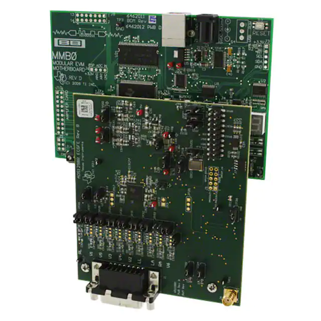
ADS1298R Hardware
Figure 1 shows the hardware included in the ADS1298R kit. Contact the factory if any component is
missing. The latest software is available on the TI website at http://www.ti.com; you should verify that you
have the latest software before using the device.
Figure 1. ADS1298R Kit
The complete kit includes the following items:
• ADS1298R ECG FE printed circuit board (PCB), Rev A
• MMB0 (Modular EVM motherboard, Rev C or higher)
SBAU181B – March 2011 – Revised Janurary 2016
Submit Documentation Feedback
Copyright © 2011–2016, Texas Instruments Incorporated
ADS1298R
9
�Quick Start
2
www.ti.com
Quick Start
This section provides a QuickStart guide to quickly begin evaluating the EVM using the ADS1298RECGFE software.
2.1
Default Jumper/Switch Configuration
Figure 2 shows the jumpers found on the ADS1298RECG-FE EVM and the respective factory default
conditions for each.
Figure 2. ADS1298RECG-FE Default Jumper Locations
Table 1 lists the jumpers and switches and the factory default conditions.
10
ADS1298R
SBAU181B – March 2011 – Revised Janurary 2016
Submit Documentation Feedback
Copyright © 2011–2016, Texas Instruments Incorporated
�Quick Start
www.ti.com
Table 1. ADS1298RECG-FE Default Jumper/Switch Configuration
Jumper
Default Position
Description
JP1
Installed
RLD feedback
JP2
Installed 1-2
AVDD selected for bipolar supply operation selected (AVDD = +2.5V)
JP3
Header Not Installed
External Vref buffer not connected
JP4
Installed
EVM +5V provided from J4 (power header)
JP5
Open
PWDN pin controlled from J5 header (pulled up to DVDD)
Header Not Installed (Pins 1-2
shorted on PCB)
DC-coupled input signals
JP15
Installed 2-3
Shield drive is open
JP16
Installed
Wilson Central Terminal (WCT) connected to INM for CH1 and CH4-8
JP17
Header Not Installed
ECG shield drive is connected to AGND
JP18
Installed 2-3
CLK connected to OSC1
JP19
Installed 1-2
OSC1 enabled
JP20
Installed 2-3
AVSS selected for bipolar supply operation (AVSS = -2.5V)
JP21
Installed 1-2
CS connected to DSP via J3.1
JP22
Installed 2-3
START comes from J3.14
JP23
Installed 1-2
CLKSEL set to 0
JP24
Installed 2-3
DVDD supply = 3.3V
JP25
Header Not Installed
No external reference selected
Installed 1-2 (top)
WCT connected to CH8- input
Installed 3-4 (bottom)
ECG_V1 connected to CH8+ input
Installed 1-2 (top)
WCT connected to CH7- input
Installed 3-4 (bottom)
ECG_V5 connected to CH7+ input
Installed 1-2 (top)
WCT connected to CH6- input
Installed 3-4 (bottom)
ECG_V4 connected to CH6+ input
Installed 1-2 (top)
WCT connected to CH5- input
Installed 3-4 (bottom)
ECG_V3 connected to CH5+ input
Installed 1-2 (top)
WCT connected to CH4- input
Installed 3-4 (bottom)
ECG_V2 connected to CH4+ input
Installed 1-2 (top)
ECG_RA connected to CH3- input
Installed 3-4 (bottom)
ECG_LL connected to CH3+ input
Installed 1-2 (top)
ECG_RA connected to CH2- input
Installed 3-4 (bottom)
ECG_LA connected to CH2+ input
Open 1-2 (top)
Not connected
Open 3-4
Not connected
Installed 5-6
CH1- input connected to source of JP35
JP6 to JP14
JP26
JP27
JP28
JP29
JP30
JP31
JP32
JP33
Installed 7-8 (bottom)
CH1+ input connected to source of JP36
JP34
Installed 1-2
Connected onboard RESP circuit to CH1- signal input mux (RESPMOD-)
JP35
Installed 1-2
Connected onboard RESP circuit to CH1+ signal input mux (RESPMOD+)
JP36
Installed 1-2
RESP control signal for U11/U12 controlled by MSP430 (U14)
SBAU181B – March 2011 – Revised Janurary 2016
Submit Documentation Feedback
Copyright © 2011–2016, Texas Instruments Incorporated
ADS1298R
11
�Quick Start
2.2
www.ti.com
ADS1298RECG-FE Operation
To prepare to evaluate the ADS1298R with the ADS1298RECG-FE, complete the following steps:
1. Verify the jumpers on the ADS1298RECG-FE are as shown in Figure 2 (note that these settings are
the factory-configured settings for the board).
2. Verify that the jumpers on the MMB0 motherboard are configured as shown below:
• MMB0 J13A → Open
• MMB0 J13B → Open
• Refer to Appendix B2 for details about the MMB0 power supply
3. Install the ADS1298RECG-FE software using the latest software version. The latest software can be
downloaded from the ADS1298RECG-FE product page. Double click the installer and follow the
instruction to complete the software installation. For detailed installation information and screenshots,
see Appendix C.
12
ADS1298R
SBAU181B – March 2011 – Revised Janurary 2016
Submit Documentation Feedback
Copyright © 2011–2016, Texas Instruments Incorporated
�Using the ADS1298RECG-FE Software
www.ti.com
3
Using the ADS1298RECG-FE Software
The ADS1298RECG-FE software provides complete control over all the settings of the ADS1298R. By
using the user interface (UI), the ADS1298R control registers can be manipulated to evaluate the various
options available on the device. Figure 3 shows the starting UI screen of the software. The UI consists of
a user menu (Section 3.1), a few top-level controls (Section 3.2), and a tabbed interface, with different
functions available on the different tabs. The tabs are:
• About (Section 3.3)
• ADC Register (Section 3.4.3)
• Analysis (Section 3.5)
• Save (Section 3.6)
Figure 3. Software Start Screen/About Tab
The user can adjust the settings when the software is not acquiring data. During acquisition, all controls
are disabled and settings may not be changed. When a setting is changed via a control, the settings are
immediately updated on the device and EVM. Settings in the software correspond to settings described in
the ADS1298R product data sheet.
SBAU181B – March 2011 – Revised Janurary 2016
Submit Documentation Feedback
Copyright © 2011–2016, Texas Instruments Incorporated
ADS1298R
13
�Using the ADS1298RECG-FE Software
3.1
www.ti.com
Application User Menu
The application user menu is located along the top of the application menu. It consists of two items: File
and Help.
File Menu (see Figure 4)
The File menu provides several options:
• Capture Screen takes a screen capture of the current view of the application and saves it as to a
file specified by the user.
• Save Configuration Settings saves the current states of the ADS1298R control registers for
reloading at a later time. This file is different from the save register on the Save tab (see
Section 3.6), which saves the current register map to a tab-delimited text file.
• Load Configuration Settings loads a previously save configuration setting file and initializes the
hardware and software to the settings within the configuration file. The configuration file must be a
file saved previously from this application using the Save Configuration Settings command, not a
file from the Save tab.
• Exit closes the application.
Help Menu (see Figure 5)
The Help menu provides the About option, which display the software and firmware version that is
currently being used. Please have this information if you need to request assistance or have a question
regarding the software or hardware.
Figure 4. User Menu - File Item
3.2
Figure 5. User Menu - Help Item
Top-Level Application Controls
Several controls/indicators are located along the top of the UI screen (see Figure 6). The controls and
indicators are described below.
Figure 6. Top Level Controls
The Data Rate indicator displays the current data rate of the ADS1298R. The data rate can be configured
in CONFIG1 control register (see Section 3.4.2.1).
The Progress indicator will display the current progress of data transfer to the PC during acquisition
cycles.
The Samples/CH control allows for the selection of the number of points, per channel, to collect during an
acquisition cycle. Keep in mind the value entered into this control in relation to the current data rate. Large
numbers of samples, coupled with slower data rates, can take time to acquire.
The ACQUIRE control starts the acquisition process. When pressed, the software will collect the
requested number of samples from the ADS1298R. All points collected during an acquisition process will
be contiguous points.
14
ADS1298R
SBAU181B – March 2011 – Revised Janurary 2016
Submit Documentation Feedback
Copyright © 2011–2016, Texas Instruments Incorporated
�Using the ADS1298RECG-FE Software
www.ti.com
The CONTINUOUS control starts a repeated acquisition process. This function acquires the requested
samples and repeats the data acquisition until the button is turned off. Within a single acquisition cycle,
the points will be contiguous, but from acquisition to acquisition, there may be points missing.
The Analysis Data input referred checkbox changes the displayed data that is read from the ADC.
Checking the box displays the data input referred, while not checking displays the data as converted.
The Show/Poll Lead Off Status displays a window (see Figure 7) that shows the status of the Lead-Off
status registers, LOFF STATP and LOFF STATN, of the ADS1298R. When the lead for the channel is
disconnected, the corresponding channel LED changes from green to red.
Figure 7. Lead-Off Status Registers Display Window
3.3
About Tab
The About tab provides software information to the user. Important safety warning, restrictions, and
disclaimers for the software and hardware are shown and should be followed during the evaluation of this
product. Additional indicators are present to provide device information (Device ID and Rev) and software
information (Firmware Version). The About tab should be the first screen displayed at startup (see
Figure 3).
SBAU181B – March 2011 – Revised Janurary 2016
Submit Documentation Feedback
Copyright © 2011–2016, Texas Instruments Incorporated
ADS1298R
15
�Using the ADS1298RECG-FE Software
3.4
www.ti.com
ADC Register Tab
The ADC Register tab provides controls to manipulate ADC control registers of the ADS1298R. Details of
the control registers are provided in the product datasheet. The ADC Register tab consists of a few
controls and several sub-tabs that further divide the control registers into different functions groups. The
sub-tabs are:
• Channel Registers tab (Section 3.4.2)
• LOFF and RLD tab (Section 3.3)
• GPIO and Other Registers tab (Section 3.4.4)
• Register Map tab (Section 3.4.5)
Figure 8. Channel Registers Tab
3.4.1
Standby and Reset Controls
The Standby control allows the user to place the ADS1298R in standby.
The Reset control allows the user to reset the ADS1298R. The Reset Mode determines which mode is
executed when the Reset control is pressed. Device Defaults resets the device to the device defaults;
Programmed Defaults resets the device, then writes the default values for using this software application.
16
ADS1298R
SBAU181B – March 2011 – Revised Janurary 2016
Submit Documentation Feedback
Copyright © 2011–2016, Texas Instruments Incorporated
�Using the ADS1298RECG-FE Software
www.ti.com
3.4.2
Channel Registers Tab (ADC Register)
The Channel Register tab provides access to control registers that control different properties/settings for
the ADC channels. The control register are grouped into two groups: Global Channel Registers and
Channel Control Registers.
3.4.2.1
Global Channel Registers
The Global Channel Registers box includes Configuration Register 1 (CONFIG1), Configuration Register 2
(CONFIG2), Configuration Register 3 (CONFIG3), and Lead Off Control Register (LOFF). The upper half
of Figure 8 shows the section of the UI panel that allows manipulation and control of these registers.
Configuration Register 1 enables the user to control the resolution mode, enable the daisy-chain
configuration options, and program the data rate.
Configuration Register 2 enables the user to select an internal square wave test source amplitude of
±1mV or ±2mV and a frequency of DC, 2Hz (fCLK/221), or 4Hz (fCLK/220).
Configuration Register 3 controls the bandgap reference (illustrated in Figure 9) and right leg drive
(RLD) options. This register enables the user to select between an external or internal reference voltage,
enable/disable the internal reference buffer, toggle between a 2.4V or a 4.0V output voltage, and to
enable/disable the RLD as well as choose whether the RLD voltage is provided internally or externally.
22mF
VCAP1
R1
(1)
Bandgap
2.4V or 4V
R3
VREFP
(1)
10mF
R2
(1)
VREFN
AVSS
To ADC Reference Inputs
Figure 9. Internal Reference and Buffer Connections
The Lead-Off Control Register allows the user to configure the threshold for the lead-off comparator,
resistive pull-up or current-source excitation, the lead-off current magnitude, and DC or AC detection.
Figure 10 illustrates a simplified diagram of the resistive pull-up and excitation options for the lead-off
detect feature.
AVDD
AVDD
ADS129x
ADS129x
10MW
INP
INP
PGA
INN
PGA
INN
10MW
a) Pull-Up/Pull-Down Resistors
b) Current Source
Figure 10. Lead-Off Excitation Options
SBAU181B – March 2011 – Revised Janurary 2016
Submit Documentation Feedback
Copyright © 2011–2016, Texas Instruments Incorporated
ADS1298R
17
�Using the ADS1298RECG-FE Software
3.4.2.2
www.ti.com
Channel Control Registers
The Channel Control Registers box allows the user to uniquely configure the front-end MUX for each ADC
channel. Additionally, at the top of the Channel Control Registers box (see Figure 8) is the option to
globally set all channels to the same setting. The channel-specific MUX is illustrated in Figure 11.
ADS129x
MUX
INT_TEST
TESTP_PACE_OUT1
INT_TEST
MUX[2:0] = 101
TestP
TempP
MvddP
(1)
MUX[2:0] = 100
MUX[2:0] = 011
From LoffP
MUX[2:0] = 000
VINP
MUX[2:0] = 110
EMI
Filter
To PgaP
MUX[2:0] = 010 AND
RLD_MEAS
MUX[2:0] = 001 (AVDD + AVSS)
2
MUX[2:0] = 111
MUX[2:0] = 000
VINN
RLDIN
From LoffN
MUX[2:0] = 001
To PgaN
MUX[2:0] = 010 AND
RLD_MEAS
RLD_REF
MvddN
(1)
TempN
MUX[2:0] = 011
MUX[2:0] = 100
MUX[2:0] = 101
TestN
INT_TEST
TESTN_PACE_OUT2
INT_TEST
Figure 11. Input Multiplexer for a Single Channel
18
ADS1298R
SBAU181B – March 2011 – Revised Janurary 2016
Submit Documentation Feedback
Copyright © 2011–2016, Texas Instruments Incorporated
�Using the ADS1298RECG-FE Software
www.ti.com
3.4.3
LOFF and RLD Tab (ADC Register)
The LOFF and RLD tab provides control over the Lead-Off Detection and Current Control Registers and
the Right Leg Derivation Control Registers. The tab and controls are shown in Figure 12.
Figure 12. LOFF and RLD Tab
3.4.3.1
Lead-Off Detection and Current Direction Control Registers
The first two arrays of controls (Lead Off Sense) enable lead-off detection for both the positive and
negative channels, LOFF_SENSP and LOFF_SENSN. By pressing the buttons, lead-off detection is
enabled for each channel individually and for each input (positive and negative). Set All LOFFP Bits and
Set All LOFFN Bits allow the user to turn on or off all the enable bits at once instead of clicking each
individual channel control.
The third array of controls (Lead Off Current Direction) determines the current direction used for lead-off
detection when an excitation signal is selected as a pull-up/pull-down resistor. Each channel is controlled
individually by selecting the button that corresponds to the desired channel to manipulate. When the
button is not illuminated, LOFF_FLIP = 0 (INP is pulled-up to AVDD and INN is pulled-down to ground).
When the button is pressed/illuminated, LOFF_FLIP = 1 (INP is pulled-down to ground and INN is pulledup to AVDD). Further details of these registers and lead-off function are located in the Applications
Section of the device data sheet.
SBAU181B – March 2011 – Revised Janurary 2016
Submit Documentation Feedback
Copyright © 2011–2016, Texas Instruments Incorporated
ADS1298R
19
�Using the ADS1298RECG-FE Software
www.ti.com
Figure 10 describes the mode for Lead-Off Detection (that is, resistive or current source) and the 4-bit
DAC settings to configure the lead-off threshold. Figure 13 illustrates the connections from the positive
and negative inputs to the lead-off comparators. The output of the comparators is viewed by using
Show/Poll Lead Off Status control as described in Section 3.2
LOFF_STATP
VINP
VINN
PGA
To ADC
LOFF_STATN
4-Bit
DAC
COMP_TH[2:0]
Figure 13. LOFF_STATP and LOFF_STATN Comparators
3.4.3.2
Right Leg Drive Derivation Control Registers
The Right Leg Drive Derivation Control Registers enable the user to set any combination of positive and/or
negative electrodes to derive the RLD voltage that is fed to the internal right leg drive amplifier.
20
ADS1298R
SBAU181B – March 2011 – Revised Janurary 2016
Submit Documentation Feedback
Copyright © 2011–2016, Texas Instruments Incorporated
�Using the ADS1298RECG-FE Software
www.ti.com
3.4.4
GPIO and OTHER Registers Tab (ADC Register)
The GPIO and Other Registers tab, located under the Analysis tab, includes controls for GPIO1 through
GPIO4, respiration phase and frequency, routing of the Wilson amplifiers, and derivation of the Goldberger
terminals. Figure 14 shows the GPIO and OTHER Registers tab and all controls contained on the tab.
Figure 14. GPIO and OTHER Register Tab
The General-Purpose I/O Register (GPIO) controls the four general-purpose I/O pins. Each GPIO can be
set as an input or an output via GPIOCx controls. If the output is selected, the GPIODx control is enabled
allowing the user to set the value to output. If the GPIO is selected as an input, the GPIODx control is
disabled and shows the value of the GPIO. If any of the GPIOs are selected as inputs, the Read GPIO
control is enabled which allows the GPIODx values to be updated to the current GPIO value.
The PACE Detect Register does not enable a special PACE measurement mode. The register allows for
enabling and configuration of the PACE amplifiers. PACE Amplifier 1 can connect to input channels 1-4
and Pace Amplifier 2 can connect to input channels 5-8.
The Configuration 4 Register allows control over the Respiration Frequency, WCT connection to the
RLD and lead-off comparator enable status.
The Respiration Control Register allows the user to configure the respiration modulation and
demodulation on Channel 1, Respiration Phase, and set the Respiration Control Signal.
SBAU181B – March 2011 – Revised Janurary 2016
Submit Documentation Feedback
Copyright © 2011–2016, Texas Instruments Incorporated
ADS1298R
21
�Using the ADS1298RECG-FE Software
3.4.4.1
www.ti.com
Wilson Central and Augmented Lead Registers
The Wilson Central Voltage (an average voltage between the right arm [RA], left arm [LA], and left leg [LL]
connections) can be derived from any combination of positive and negative terminals from channels 1-4
and routed to the WCT pin. Likewise, the Augmented Leads (AVF, AVL, AVR) may be derived from
channels 1-4 and routed to the negative terminal of channels 5, 6, and 7. Figure 15 shows these
configurations; Figure 15a illustrates the central lead routing, and Figure 15b shows the augmented lead
routing.
(b) Wilson Augmented Lead Routing
(a) Wilson Central Lead Routing
IN1P
IN1N
IN2P
IN2N
IN3P
IN3N
IN4P
IN4N
To Channel
PGAs
8:1 MUX
8:1 MUX
Wcta
Wctb
8:1 MUX
WCT2[2:0]
Wctc
8:1 MUX
WCT2[5:3]
30kW
8:1 MUX
WCT1[2:0]
30kW
Wctb
To Channel
PGAs
8:1 MUX
WCT2[2:0]
WCT2[5:3]
WCT1[2:0]
Wcta
IN1P
IN1N
IN2P
IN2N
IN3P
IN3N
IN4P
IN4N
Wctc
avF_ch4
30kW
WCT
ADS1298
80pF
AVSS
ADS1294/6/8
avF_ch6
avF_ch5
avF_ch7
IN5P
IN5N
IN6P
IN6N
IN7P
IN7N
To Channel
PGAs
Figure 15. Wilson Central and Augmented Lead Routing Diagrams
22
ADS1298R
SBAU181B – March 2011 – Revised Janurary 2016
Submit Documentation Feedback
Copyright © 2011–2016, Texas Instruments Incorporated
�Using the ADS1298RECG-FE Software
www.ti.com
3.4.5
Register Map (ADC Register)
The Register Map tab is a helpful debug feature that allows the user to view the state of all the internal
registers. This tab is illustrated in Figure 16. Refresh Registers control updates the register map values
with the current register settings of the ADS1298R.
Figure 16. Device Registers Settings
SBAU181B – March 2011 – Revised Janurary 2016
Submit Documentation Feedback
Copyright © 2011–2016, Texas Instruments Incorporated
ADS1298R
23
�Using the ADS1298RECG-FE Software
3.5
www.ti.com
Analysis Tab
The Analysis tab provides access to the different analysis options that are available using the software.
The different analyses are grouped by sub-tabs:
• Scope tab (Section 3.5.1)
• Histogram tab (Section 3.5.2)
• RESP tab (Section 3.5.4)
• FFT tab (Section 3.5.3)
• ECG tab (Section 3.5.5)
3.5.1
Scope Tab (Analysis)
The Scope tool is useful for examining the exact amplitude of the measured input signals from each
channel. Additionally, users can determine the noise contribution from each channel at a given resolution,
and review the sampling rate, the PGA gain, and the input signal amplitude. Figure 17 illustrates the
Scope tool features.
Figure 17. Scope Tool Features
In the Scope Analysis window, as Figure 18 illustrates, the different noise levels are displayed when the
MUX is selected as Input Short, PGA gain is set to 6 (default), and the sample rate is set to 500 samples
per second (SPS).
Figure 18. Scope Analysis Tab (Noise Levels for Each Channel Shown)
24
ADS1298R
SBAU181B – March 2011 – Revised Janurary 2016
Submit Documentation Feedback
Copyright © 2011–2016, Texas Instruments Incorporated
�Using the ADS1298RECG-FE Software
www.ti.com
3.5.1.1
Zoom Tool
The zoom tool allows the user to zoom in either on all channels simultaneously or on a single channel.
Figure 19 shows an example of the waveform examination tool with the magnifying glass zoomed in on
Channel 2. In this case, the tool makes it much easier to determine that the noise seen on the ECG
waveform is a result of 50Hz/60Hz line cycle noise.
Figure 19. Zoom Tool Options
SBAU181B – March 2011 – Revised Janurary 2016
Submit Documentation Feedback
Copyright © 2011–2016, Texas Instruments Incorporated
ADS1298R
25
�Using the ADS1298RECG-FE Software
3.5.2
www.ti.com
Histogram Tab (Analysis)
The Histogram tool is used primarily to see the bin separation of the different amplitudes of the ECG
waveform harmonics. Figure 20 illustrates the histogram output for a 12-lead signal. The same ECG
Signal Zoom analysis may be used on the histogram plots for a more detailed examination of the
amplitude bins.
Figure 20. Histogram Bins for 12-Lead ECG Signal
Figure 21 shows the Histogram Analysis window that is displayed when the Histogram Analysis button
(at the bottom of the screen in Figure 20) is clicked. The analysis window shows the mean, VRMS, and VPP
channel amplitude bins.
Figure 21. Statistics for the Signal Amplitude of Eight ECG Channels
26
ADS1298R
SBAU181B – March 2011 – Revised Janurary 2016
Submit Documentation Feedback
Copyright © 2011–2016, Texas Instruments Incorporated
�Using the ADS1298RECG-FE Software
www.ti.com
3.5.3
FFT Tab
The FFT tool allows the user to examine the channel-specific spectrum as well as typical figures of merit
such as SNR, THD, ENOB, and CMRR. Each feature is numbered below and described in detail in the
following subsections. Figure 22 illustrates an FFT plot for a normal electrode configuration.
Figure 22. FFT Graph of Normal Electrode Configuration
1 - Coherent Frequency Calculator
Coherent sampling in an FFT is defined as FAIN/FSAMPLE = NWINDOW/NTOTAL, where:
• FAIN is the input frequency
• FSAMPLE is the sampling frequency of the ADS1298R
• NWINDOW is the number of odd integer cycles during a given sampling period
• NTOTAL is the number of data points (in powers of 2) that is used to create the FFT
If the conditions for coherent sampling can be met, the FFT results for a periodic signal will be
optimized. The Ideal AIN Frequency is a value that is calculated based on the sampling rate, such that
the coherent sampling criteria can be met.
2 - AC Analysis Parameters
This section of the tool allows the user to dictate the number of harmonics, DC leakage bins, harmonic
leakage bins, and fundamental leakage bins that are used in the creation of various histograms.
Pressing the Windowing button, illustrated in Figure 23, allows the user to evaluate the FFT graph
under a variety of different windows. Note that pressing the Reference button toggles between dBFS
(decibels, full-scale) and dBc (decibels to carrier).
Figure 23. AC Analysis Parameters: Windowing Options
SBAU181B – March 2011 – Revised Janurary 2016
Submit Documentation Feedback
Copyright © 2011–2016, Texas Instruments Incorporated
ADS1298R
27
�Using the ADS1298RECG-FE Software
www.ti.com
3 - FFT Analysis
Pressing the FFT Analysis button pulls up the FFT Analysis window shown in Figure 24. This window
provides calculated parameters obtained from the collected data that may be useful during evaluation.
One of the values included in this analysis is the channel-to-channel noise.
Figure 24. FFT Analysis: Input Short Condition
4 - User-Defined Dynamic Range
This section enables the user to examine the SNR of a specific channel within a given frequency band
defined by Low Frequency and High Frequency. The SNR displayed in this window shows under the
Dynamic Range heading as Figure 25 illustrates.
Figure 25. Changing the User-Defined Dynamic Range for Channel 1
5 - Input Amplitude
This field is a user input that is important for accurately calculating the CMRR of each channel.
6 - Zoom Tool
As with the Analysis, Histogram, and Scope tool, this zoom function allows a closer examination of the
FFT at frequencies of interest, as shown in Figure 26.
28
ADS1298R
SBAU181B – March 2011 – Revised Janurary 2016
Submit Documentation Feedback
Copyright © 2011–2016, Texas Instruments Incorporated
�Using the ADS1298RECG-FE Software
www.ti.com
Figure 26. FFT Plot Using Zoom Tool
SBAU181B – March 2011 – Revised Janurary 2016
Submit Documentation Feedback
Copyright © 2011–2016, Texas Instruments Incorporated
ADS1298R
29
�Using the ADS1298RECG-FE Software
3.5.4
www.ti.com
RESP Tab
The Resp tool allows the user to make use of the on-board respiration circuitry to show a simulated
respiration signal. Respiration Tab shows the RESP tab tool features.
Respiration Tab
The bottom left portion of the screen provides controls that may be utilized to add filtering to the displayed
respiration signal. NOTE: The filtering performed using this analysis tool is performed in the UI software
and is not available in the ADS1298R device. The Low Pass Filter group of controls implement a lowpass digital filter on the collected data. The filter is enabled using the Enable control, and Filter Order
and Cutoff Frequency allow for the customization of the filter. The High Pass Filter group of controls
implement a digital high-pass filter on the collected data. The high-pass controls function the same as the
low-pass controls except that they apply to the high-pass filter. The Unsettled Points to Remove control
allows the user to remove a specific number of points from the beginning of the filtered data set. This
allows the user to remove the data the isn't filtered and look only at the filtered data.
The Simulated Respiration Frequency set the respiration frequency that the on-board respiration
circuitry will simulate when collecting data.
The Statistical Data group provides two calculated parameters from the displayed data, Mean and Noise.
30
ADS1298R
SBAU181B – March 2011 – Revised Janurary 2016
Submit Documentation Feedback
Copyright © 2011–2016, Texas Instruments Incorporated
�Using the ADS1298RECG-FE Software
www.ti.com
3.5.5
ECG Tab (Analysis)
This tool allows the user to examine the input signal according to the different lead configurations. For a
detailed description of the lead configurations, see Table 2 in Section 4.6. Figure 27 shows Leads I-III and
the Augmented Lead outputs with the input MUX configured in Normal Electrode mode. Figure 27 also
shows numerical annotations 1 to 4, which highlight the different features of this tool. These features are
described in detail in the following subsections.
Figure 27. ECG Display Tab Showing LEAD I-III and Augmented Leads
1 - Plot Set Selection Feature
The Plot Set Selection control allows the user to change the visual selection between:
• Limbs and Augmented Leads displays LEAD I, LEAD II, LEAD III, aVR, aVL, and AVF signals,
• Chest Leads displays V1 - V6 signals.
NOTE: For display that shows 6 leads combined, the ECG signals have any DC offset removed and
a different offset added to the signal to display the signals as shown. To see the raw ECG
data, you can select the individual signals as described below in the Zoom feature (box 4).
2 - ECG Separation Feature
The ECG separation control toggles the vertical distance between the input plots. This capability is
useful when ECG signals are large and require more separation to avoid overlap, or to collapse the
range between signals when the ECG signals are small.
3 - Post Processing Filters Feature
The Post Processing Filters Features controls provides a low-pass, a 50Hz/60Hz notch, and a highpass digital filters for post-processing the data from the ADS1298R. To activate each filter, the Enable
checkbox should be checked. To disable the filter, the Enable checkbox should be unchecked. Any
combination of the three digital filters can be used by enabling the respective filter.
SBAU181B – March 2011 – Revised Janurary 2016
Submit Documentation Feedback
Copyright © 2011–2016, Texas Instruments Incorporated
ADS1298R
31
�Using the ADS1298RECG-FE Software
www.ti.com
The low-pass filter controls a digital low-pass filter, whose order and cutoff frequency are controlled
using the Filter Order and Cutoff Freq controls in the low-pass filter part of the Post Processing
Filters group (left side of the box).
The notch filter provides a 50Hz/60Hz notch filter, whose order and 50Hz/60Hz notch selection are
controlled using the Filter Order and Notch Freq controls in the low-pass filter part of the Post
Processing Filters group (center of the box).
The high-pass filter controls a digital high-pass filter, whose order and cutoff frequency are
controlled using the Filter Order and Cutoff Freq controls in the high-pass filter part of the Post
Processing Filters group (right side of the box).
NOTE: The digital filters are not part of the ADS1298R. These are digital filters implemented in the
UI to aid in the evaluation of the ADS1298RECG-FE.
4 - Zoom Feature
The zoom feature is available to allow the user to navigate and view all signals at the same time, as
shown in Figure 28. This tool allows the user to zoom in/out on the horizontal or vertical axis and pan
left or right while viewing all ECG signals simultaneously.
Figure 28. ECG Signal Zoom Feature for Six Leads
Additionally, each ECG signal can be zoomed individually by moving the mouse (which appears as a plus
icon) over the lead of interest and clicking on it. A new window opens showing the raw ECG data as read
from the ADS1298R. This window provides controls in the lower right corner to zoom in/out or pan
right/left to provide a more detailed inspection of the individual ECG signal.
Figure 29. ECG Signal Zoom Feature for Lead 1
32
ADS1298R
SBAU181B – March 2011 – Revised Janurary 2016
Submit Documentation Feedback
Copyright © 2011–2016, Texas Instruments Incorporated
�Using the ADS1298RECG-FE Software
www.ti.com
3.6
Save Tab
The Save tab provides the user the ability to save the collected data for a record of the evaluation or
further analysis. Reference the previous sections for the list of the analysis data available for each
analysis.
The Analysis to Save group allows the user to save the different analysis calculations that were performed
on the data.
• Scope Analysis saves the scope analysis data available from the scope analysis pop-up window
• FFT Analysis saves the FFT analysis data available from the FFT analysis pop-up window.
• Histogram Analysis saves the histogram analysis data available from the histogram analysis pop-up
window.
• Register Settings saves the current settings from the register map and can be useful to obtain the
register values for your specific device configuration. Saving the register map in this format is not be
confused with saving your register settings for reloading into the software at another time (see
Section 3.1).
Each item will be saved if the corresponding checkbox is checked.
The Data to Save group allows the user to save the various data sets collected from the ADS1298R. The
CH x controls allow the user to specify which channels will be saved for each of the data selections made.
• Data - Codes selects the raw data (in codes format) to be saved to a file.
• Data - Volts selects the raw data (converted to voltage) to be saved to a file.
• FFT Data selects the calculated FFT data to be saved to a file. Note: This is not raw data; it is the
frequency bin and magnitude data that was calculated by the UI.
• Histogram Data selected the calculated Histogram data to be saved to a file. Note: This is not raw
data; it is the code bin and number of occurrences data that was calculated by the UI.
The User Comments/Notes group allows the user to indicate a Record Number and User Comments
that are saved with each file. This data permits the user to distinguish different data sets from one
another.
The Directory to Save Files is the directory where all the saved files will be placed. The user can select a
directory by pressing the folder button (located to the right of the control). Each data file that is saved is
automatically named to prevent overwriting of files.
The Save To File button saves all the data files that were selected using the check boxes to the selected
directory.
SBAU181B – March 2011 – Revised Janurary 2016
Submit Documentation Feedback
Copyright © 2011–2016, Texas Instruments Incorporated
ADS1298R
33
�Using the ADS1298RECG-FE Software
www.ti.com
Figure 30. Save Tab
34
ADS1298R
SBAU181B – March 2011 – Revised Janurary 2016
Submit Documentation Feedback
Copyright © 2011–2016, Texas Instruments Incorporated
�ADS1298RECG-FE Input Signals
www.ti.com
4
ADS1298RECG-FE Input Signals
NOTE: Before evaluating specific ECG functions, it is recommended that the user acquire data with
inputs shorted internally. This configuration ensures that the board is operating properly.
4.1
Input Short Testing
By default, the EVM powers up with the individual channels to an internal short with a data rate of 500SPS
and a PGA gain of 6. Once the Acquire button is pressed, the Scope Analysis should reflect inputreferred VPP values less than 5µVPP
4.2
Internal Test Signals Input
Configuration Register 2 controls the signal amplitude and frequency of an internally-generated square
wave test signal. The primary purpose of this test signal is to verify the functionality of the front-end MUX,
the PGA, and the ADC. The test signals may be viewed on the ECG Display tab, as Figure 31 shows.
Detailed instructions for using the ECG Display tab are provided in Section 3.5.5.
Figure 31. Example of Internal Test Signals Viewed on the ECG Display Tab
SBAU181B – March 2011 – Revised Janurary 2016
Submit Documentation Feedback
Copyright © 2011–2016, Texas Instruments Incorporated
ADS1298R
35
�ADS1298RECG-FE Input Signals
4.3
www.ti.com
Temperature Sensor
The internal temperature sensor on the ADS1298R is shown in Figure 32. When the internal MUX is
routed to the temperature sensor input, the ADC internal temperature is calculated from the ADC output
voltage using Equation 1.
AVDD
1x
2x
8x
1x
AVSS
Figure 32. Internal Temperature Sensor
Temperature (°C) =
Temperature Reading (mV) - 145,300mV
490mV/°C
+ 25°C
(1)
The ADC can be configured to give a temperature reading by selecting the Temperature Sensor option on
the Channel Control Registers GUI (see Section 3.4.2.2) and verified using the Scope tab as shown in
Figure 33. The number 0.1447V (on the y-axis) can be calculated as a temperature using Equation 1:
Temperature = (0.1447 – 0.145300) / 0.00049 + 25 = 23.78°C
A more detailed description of the Scope tab is provided in Section 3.5.1.
Figure 33. Eight-Channel Read of Internal Temperature
36
ADS1298R
SBAU181B – March 2011 – Revised Janurary 2016
Submit Documentation Feedback
Copyright © 2011–2016, Texas Instruments Incorporated
�ADS1298RECG-FE Input Signals
www.ti.com
4.4
Normal Electrode Input
The Normal Electrode input on the MUX routes the inputs (VINP and VINN) differentially to the internal
PGA, as Figure 11 illustrates. In this mode, an ECG, sine wave, or pulse generator may be connected to
test the ADS1298R.
Figure 34 shows a typical six-lead output when connected to a 5mVPEAK, 80BPM ECG signal.
Figure 34. Normal Electrode ECG Connection in ECG Display Tab
4.4.1
Capturing 12-Lead ECG Signals
To capture signals from external inputs:
1. Configure the Channel Input control in Globally Set Channels to Normal Electrode.
2. Connect the 10 ECG electrodes from the Fluke simulator to the EVM through the DB15 connector (J1).
Refer to Section A.3 for the ECG cable details. The ECG electrode signals are passed through a single
pole RC filter followed by the lead configuration. For ECG signal processing, the electrode signals are
routed through J5 to the ADS1298R input. The signal path in the board can be chosen by jumper
settings, depending on the application.
4.5
MVDD Input, RLD Measurement, RLD Positive Electrode Driver, and RLD Negative
Electrode Driver
The MVDD input option allows the measurement of the supply voltage VS = (AVDD + AVSS)/2 for channels 1,
2, 5, 6, 7, and 8; however, the supply voltage for channel 3 will be DVDD/2. As an example, in bipolar
supply mode, AVDD = 3.0V and AVSS = –2.5V. Therefore, with the PGA gain = 1, the output voltage
measured by the ADC will be approximately 0.25V.
The RLD measurement takes the voltage at the RLDIN pin and measures it on the PGA with respect to
(AVDD + AVSS)/2. This feature is beneficial if the user would like to optimize the gain of the RLD loop.
SBAU181B – March 2011 – Revised Janurary 2016
Submit Documentation Feedback
Copyright © 2011–2016, Texas Instruments Incorporated
ADS1298R
37
�ADS1298RECG-FE Input Signals
www.ti.com
The voltage used to derive the right leg drive for both the positive and negative electrodes may also be
measured with respect to (AVDD + AVSS)/2.
4.6
Lead Derivation
The EVM is configured to generate the 12 ECG signals using 10 electrodes connected to the eight ADC
channels. Lead I, Lead II, and V1-V6 are computed in the analog domain, while the augmented leads and
Lead III are computed digitally. The channel assignments are described in Table 2.
• LA = Left Arm
• LL = Left Leg
• RA = Right Arm
Table 2. ADS1298R Lead Measurements
Lead (1)
ADS1298R Input Channels
(1)
1
V6 = V6 – WCT
2
LEAD I = LA – RA
3
LEAD II = LL – RA
4
V2 = V2 – WCT
5
V3 = V3 – WCT
6
V4 = V4 – WCT
7
V5 = V5 – WCT
8
V1 = V1 – WCT
WCT = (LA + RA + LL)/3
Table 3. Derived Lead Calculations
Derived Lead
Formula Used to Calculate
LEAD III
4.7
LL - RA - LA = LEAD II - LEAD I
aVR
RA - (LA + LL) / 2 = - (LEAD I + LEAD II) / 2
aVL
LA - (RA +LL) / 2 = LEAD I - LEAD II / 2
aVF
LL - (RA + LA) / 2 = LEAD II - LEAD I /2
Wilson Center Terminal (WCT)
The Wilson Center Terminal voltage is internally generated by the ADS1298R device. The WCT1 and
WCT2 registers provide controls to select any of the eight inputs (CH1P to CH4P, CH1M to CH4M) for
routing to the three integrated WCT amplifiers.
The ADS1298RECG-FE is configured for 12-lead ECG inputs, with the limb electrodes connected as
shown in Table 2. During EVM power-up, the firmware configures the device to route CH2P, CH2M, and
CH3P (RA, LA, LL) to the internal buffers. This configuration generates a signal at the WCT pin equal to
(RA + LA + LL)/3. By installing JP16, the WCT is routed to the single-ended channels to achieve the
desired signals.
4.8
Right Leg Drive
The RL electrode is driven directly by the RLD signal generated on-chip by the ADS1298R. The bandwidth
of the RLD loop is determined by R8 (392kΩ) and C20 (10nF). Users can change these values to set the
bandwidth based on their specific application. The loop stability is determined by the user’s specific
system. Therefore, adjustment of the feedback component values may be required to ensure stability if
additional filtering components and long cables are added before the ADS1298RECG-FE.
In a typical application, the RLD signal is implemented as the average of RA, LA, and LL. For system
flexibility, the ADS1298R allows the user to select any combination of the electrodes to generate the RLD
(see ADS1298R data sheet for more details).
38
ADS1298R
SBAU181B – March 2011 – Revised Janurary 2016
Submit Documentation Feedback
Copyright © 2011–2016, Texas Instruments Incorporated
�ADS1298RECG-FE Input Signals
www.ti.com
4.8.1
RLD Common Mode Voltage
The RLD common mode voltage can be set to (AVDD+AVSS)/2 or to an externally provided source. If the
application requires the common mode to be set to any voltage other than mid-supply, this can be
accomplished by setting the appropriate bit in the Configuration 3 Register. On the ADS1298ECG-FE, the
external RLDREF voltage is set using resistor R1 and adjustable resistor R2 (R1 and R2 are not installed
by default).
During power-up, the firmware configures the device for internal RLDREF operation. To configure the RLD
circuitry manually, use the following steps and the controls found on the ADC Register tab.
1. Verify that the Channel Input is set to the Normal Electrode mode for all channels (Channel
Registers tab).
2. In CONFIG3 control register (Channel Registers tab):
• Enable the RLD Buffer (RLD Buffer Power = Enable)
• Set the internal RLD reference (RLDREF Signal Source)
3. Select the electrodes for the RLD loop from the Right Leg Drive Derivation Control Registers controls
(LOFF and RLD tab)
Once these steps are completed, measure and verify that the voltage on either side of R38 is close to
mid-supply. This measurement confirms whether the RLD loop is functional.
The on-chip RLD signal can be fed back into the ADS1298R by shorting JP1. This RLD signal can then be
sent to the ADC (to measure for debug purposes) or to other electrodes for driving (to change the
reference drive in case the RL electrode falls off). Refer to the ADS1298R product data sheet for
additional details.
4.8.2
Driving the RLD Cable Shield
Apart from the RLD signal, the ADS1298RECG-FE also offers three options to drive the cable shield:
• In-phase RLD signal
• Out-of-phase RLD signal
• Board AGND
Table 4 summarizes the configuration of JP15 and JP17 for each of the options.
Table 4. RLD Jumper Options
4.9
ECG Cable
ELEC_SHD signal
JP15
JP17
AGND
1-2
Don't Care
RLD (0: In phase)
2-3
2-3
RLD (180: Out of phase)
2-3
1-2
PACE Detection
The ADS1298R supports data rates up to 32kSPS for software PACE detection, which typically requires a
data rate of at least 8kSPS.
NOTE: The ADS1298RECG-FE does not include software PACE detection algorithms.
The ADS1298R provides the user the flexibility of doing hardware PACE detection with external circuitry.
PACE detection can be done simultaneously on two channels: one from the odd channels and one from
the even channels. Refer to the ADS1298R product data sheet for additional details.
To turn on the PACE buffer and select the channels, set the PACE Register from the GPIO and OTHER
Registers tab. The PGA outputs of the selected channels are available at connector J5, pins 1 and 2.
SBAU181B – March 2011 – Revised Janurary 2016
Submit Documentation Feedback
Copyright © 2011–2016, Texas Instruments Incorporated
ADS1298R
39
�ADS1298RECG-FE Input Signals
www.ti.com
Figure 35 shows an example waveform created by a Fluke Medsim 300B processed by the ADS1298R at
a data rate of 8kSPS. Using higher data rates increases power consumption because all channels must
sample at this data rate simultaneously; thus, the PACE buffers offer the flexibility to process PACE
signals separately from the ADS1298R. The signal must be AC coupled to obtain the waveform\ shown
below.
Figure 35. Digitization of PACE Signal Using ADS1298R
40
ADS1298R
SBAU181B – March 2011 – Revised Janurary 2016
Submit Documentation Feedback
Copyright © 2011–2016, Texas Instruments Incorporated
�Evaluation of the ADS1298R Respiration Function
www.ti.com
5
Evaluation of the ADS1298R Respiration Function
5.1
Introduction
The ADS1298R allows for the measurement of respiration rate based on the principle of impedance
pneumography. The key concept of this approach is to measure the change in impedance of the thoracic
cavity during breathing (respiration). The ADS1298REVM provides two ways to test the respiration
circuitry: first, using onboard circuitry; and second, using a patient simulator with respiration outputs. This
section describe both approaches.
5.2
Testing with Onboard Circuitry
For additional information on Impedance Pneumography, please refer to the following application note.
5.2.1
Hardware Configuration
The ADS1298REVM has onboard circuitry to test a respiration circuit. A simplified diagram illustrating only
the respiration portion of the circuit is shown in Figure 36; the onboard circuitry to generate the respiration
signal is within the red dotted box. By default, jumpers JP34 and JP35 connect the onboard circuitry for
respiration evaluation. R77 models the baseline impedance of the thoracic cavity. This component is a
surface-mount resistor located on the underside of the board; it can be changed if desired. R78 and R79
model the cable resistance (typically 1kΩ for patient monitoring). Capacitors C97 and C98 are used to
model the parasitic capacitance that may be present when real cables are used. Capacitors C113 and
C114 serve as a secondary means to prevent a single fault (such as a shorted C112 capacitor from a
carrier generator) from causing excessive DC currents through the electrodes.
The parameter of interest is the change in impedance during breathing. This change in impedance is
accomplished by switching 1MΩ impedance in parallel to R77 using an analog switch, U11. Two 1MΩ
resistors (R82 and R83) have been added to provide a DC bias to this switch. Switch U11 must have a
control signal that toggles between AVSS and AVDD at the desired respiration frequency. This control
signal can be fed from either an onboard signal source or an external function generator via JP36.
Figure 36. Respiration Evaluation with Onboard Circuitry
SBAU181B – March 2011 – Revised Janurary 2016
Submit Documentation Feedback
Copyright © 2011–2016, Texas Instruments Incorporated
ADS1298R
41
�Evaluation of the ADS1298R Respiration Function
www.ti.com
The remainder of the circuit is necessary for respiration measurements with both the onboard circuitry and
patient simulator. Resistors R96 and R97 limit the amount of AC current that flows into the body.
Capacitors C108 and C109 block any DC current from flowing into the body from the transmission side.
Capacitors C99 and C100 serve the same purpose on the receiver side. The respiration capability is
available on Channel 1. The respiration signals are routed to Channel 1 when the two shunts on JP33 are
in the respective default locations, shorting pins 5-6 and 7-8 as shown in Figure 36.
5.2.2
Software Configuration
The Respiration Control Register works in conjunction with Configuration Register 4 (CONFIG4). Certain
bit changes must be done in order to activate the respiration circuitry of the ADS1298R.
For internal respiration with an internal clock, set the following:
• Configuration Register 4
– Respiration Frequency to 32kHz
• CHxSET registers
– Normal Electrode
– Gain to 6
• RESP register set to:
– Respiration Demodulation to Enabled
– Respiration Modulation to Enabled
– VREF to VREFP
– Respiration Phase to 112.5 deg
– Respiration Control to Internal Respiration with Internal Clock
Next, switch U11 must be toggled at the desired respiration frequency by applying a square wave via
JP36. An onboard MSP430G2121 is provided to give approximately 0.1Hz through 0.5Hz. The MSP430
circuitry is selected when JP36 is loaded with a shunt jumper that shorts pins 1-2 (default). An external
function generator can also be used for this purpose by applying a signal to SMA connector J6 and
moving the shunt jumper on JP36 to cover pins 2-3. Data can be acquired by clicking on the Acquire tab.
Figure 37 shows the results for a 0.5Hz toggling of the switch.
The expected DC output can be calculated using Equation 2.
R77 + R78 +R79
· (VREFP - VREFM)
DC_V =
R96 + R97 + R77 + R78 +R79
DC_V =
0.33k + 1k +1k
· 2.4 = 67.9mV
40k + 40k + 0.33k + 1k +1k
(2)
The expected peak-to-peak output as a result of the impedance change can be calculated with
Equation 3; this value is the current flowing through the body:
2.4
VREFP - VREFM
IB =
= 29.15mA
=
R77 + R78 + R79 + R96 + R97 82.33k
(3)
The Δ impedance and peak-to-peak output can be calculated with Equation 4 and Equation 5.
DR = R77 - R77 || R76 = 330 - 329.89 = 0.11W
(4)
DV = DR · IB = 0.11 · 29.15 = 3.2mV
(5)
The results shown in Figure 37 are taken using a data rate of 500SPS. To obtain better resolution, these
results must be low-pass filtered. Figure 38 shows the result after the signal has been processed through
a 2Hz low-pass filter.
42
ADS1298R
SBAU181B – March 2011 – Revised Janurary 2016
Submit Documentation Feedback
Copyright © 2011–2016, Texas Instruments Incorporated
�Evaluation of the ADS1298R Respiration Function
www.ti.com
Figure 38. Results After Low-Pass Filtering
Figure 37. Channel 1 Δ Impedance Measurement
SBAU181B – March 2011 – Revised Janurary 2016
Submit Documentation Feedback
Copyright © 2011–2016, Texas Instruments Incorporated
ADS1298R
43
�Evaluation of the ADS1298R Respiration Function
5.3
5.3.1
www.ti.com
Testing with Patient Simulator
Hardware Configuration
The output from any typical patient simulator can be directly fed into the DB15 connector. The shunts on
jumpers JP34 and JP35 should be moved from the respective default positions (shorting pins 1-2) so that
these components now short pins 2-3.
5.3.2
Software Configuration
We then must write to the following registers before we take any data. Under the ADC Register, Channel
Registers tab, the Global Channel Registers should be configured to the software default configuration
(see Section 3.4.1 for further details on software default configuration).
For internal respiration with an internal clock, set the following:
• Channel Control Registers control
– Channel Input to Normal Electrode
– Gain to 6
• Configuration Register 4
– Respiration Frequency to 32kHz
– Pulse Mode Enabled to Disable
– Lead-off Comparator Power-down to Enable
• RESP register set to:
– Respiration Demodulation to Enable
– Respiration Modulation to Enable
– VREF to VREFP
– Respiration Phase to 112.5 deg
– Respiration Control to Internal Respiration with Internal Clock
There are several options that permit users to choose different base impedance (RB) and delta impedance
(ΔR) on the simulator. For illustration purposes, a base impedance RB of 500Ω is chosen.
Figure 39 shows the results with RB= 500Ω and ΔR = 1Ω. The expected DC output can be calculated with
Equation 6:
RB
· (VREFP - VREFM)
DC_V =
RB + R96 +R97
DC_V =
44
0.5k
· 2.4 = 14.9mV
0.5k + 40k + 40k
(6)
Current flowing through the body is calculated by Equation 7:
2.4
VREFP - VREFM
IB =
= 29.81mA
=
80.5k
R96 + R97 + RB
(7)
The peak-to-peak output can then be calculated as shown in Equation 8:
DV = DR · IB = 1 · 29.15 = 29.1mV
(8)
ADS1298R
SBAU181B – March 2011 – Revised Janurary 2016
Submit Documentation Feedback
Copyright © 2011–2016, Texas Instruments Incorporated
�Evaluation of the ADS1298R Respiration Function
www.ti.com
Figure 39 and Figure 40 show the results with RB = 500Ω and ΔR = 1Ω and with RB= 500Ω and ΔR =
0.1Ω, respectively.
Figure 39. Channel 1 Result for RB= 500Ω and ΔR = 1Ω
Figure 40. Channel 1 Result for RB= 500Ω and ΔR = 0.1Ω
These two approaches to performing respiration measurements show that the internal respiration circuitry
of the ADS1298R can resolve down to 100mΩ.
SBAU181B – March 2011 – Revised Janurary 2016
Submit Documentation Feedback
Copyright © 2011–2016, Texas Instruments Incorporated
ADS1298R
45
�ADS1298R Daughter Card Hardware Details
6
www.ti.com
ADS1298R Daughter Card Hardware Details
The ADS1298RECG front-end evaluation board is configured to be used with the TI MMB0 data converter
evaluation platform. The ADS1298RECG-FE board is a four-layer circuit board. The board schematic and
layout are provided in Appendix A.
The ADS1298R can be used as a demonstration board for standard, 12-lead ECG applications with an
input configuration of 10 electrodes. Users can also bypass the 12-lead configuration and provide any type
of signal directly to the ADS1298R through a variety of hardware jumper settings (JP26-JP33; see
Section A.2). External support circuits are provided for testing purposes such as external references,
clocks, lead-off resistors, and shield drive amplifiers.
Figure 41 shows the functional block diagram with important jumper names for the EVM.
ADS1298REVM
Power
Connector
J4
Shield
Drive
ADS1298R Signals
Connectors
Power
Mgmt
High-pass
Filter
Right Leg
Electrodes
MMB0/C5505 Interface
Connectors
ADS1298R
ECG SOC
JP6 to
J14
Input Signal
Connector
3 Limb and
6 Chest
J1 Electrodes
Diode Clamp
Low-pass Filter
DB Connector for
10 ECG Electrodes
Shield
JP26JP33
JP3
External
Reference
(optional)
JP18
External
Clock
(optional)
Figure 41. ADS1298R Front-End Block Diagram
6.1
Jumper Description
Table 5 shows the jumpers on the ADS1298RECG-FE and options available for each jumper.
Table 5. ADS1298RECG-FE Default Jumper/Switch Configuration
(1)
46
Jumper
Function
Settings
JP1
Installed
RLD feedback
JP2
AVDD supply source
1-2: AVDD selected for bipolar supply operation (AVDD = +2.5V)
2-3: AVDD selected for single supply operation (AVDD = +3.0V)
JP3
External Reference Connection
(Header Not Installed) (1)
Open: External reference not connected
Installed: External reference connected
JP4
Connect EVM +5V rail to
J4(power header)
Open: EVM +5V must be supplied externally
Installed: EVM +5V supplied from J4 (power header)
JP5
PWDN source
Open: PWDN pin controlled from J5 header (pulled up to DVDD)
Installed: Device is powered down (PWDN pin = AGND)
JP6 to
JP114
Input signal DC/AC couples
(Header Not Installed)
1-2: DC-coupled input signals (Pins 1-2 shorted on PCB)
2-3: AC-coupled input signals (Requires installation of header and cutting PCB
short of pin 1-2)
JP15
ECG shield drive connected
1-2: ECG shield is grounded (AGND)
2-3: ECG shield is connected to buffer (required U2 installation, otherwise shield
connection is open)
JP16
Wilson Central Terminal (WCT)
connection
Open: WCT NOT connected to JP26-30 and JP33
Installed: WCT connected to JP26-30 and JP33 for connection to CH1 and CH4-8
IN-
Requires installation of JP25 and references U3/U4
ADS1298R
SBAU181B – March 2011 – Revised Janurary 2016
Submit Documentation Feedback
Copyright © 2011–2016, Texas Instruments Incorporated
�ADS1298R Daughter Card Hardware Details
www.ti.com
Table 5. ADS1298RECG-FE Default Jumper/Switch Configuration (continued)
Jumper
Function
Settings
JP17
ECG shield drive buffer
input(Header Not Installed) (2)
1-2: ECG shield drive connected to RLDOUT
2-3: ECG shield drive connected to RLDINV
JP18
CLK connection
1-2: CLK connected to DSP (J3.17)
2-3: CLK connected to OSC1
JP19
OSC1 Enable
1-2: OSC1 enabled
2-3: OSC1 disabled
JP20
AVSS supply source
1-2: AVSS selected for single supply operation (AVSS = 0V (AGND))
2-3: AVSS selected for bipolar supply operation (AVSS = -2.5V)
JP21
CS source
1-2: CS connected to DSP via J3.1
2-3: CS connected to DSP via J3.7
JP22
START source
1-2: START comes from J3.1
2-3: START comes from J3.14
JP23
CLKSEL source
1-2: External Master Clock
2-3: Internal Master Clock (CLKSEL controlled by J3.2 (pulled up to DVDD))
JP24
DVDD Supply Select
1-2: DVDD supply = 1.8V
2-3: DVDD supply = 3.3V
JP25
External Reference Selection
(Header Not Installed) (3)
1-2: Select U4 as reference source
2-3: Selected U3 as reference source
1-2: CH8- connection
Open: Channel input not connected
Installed: Channel input connected to WCT (requires JP16 to be installed)
3-4: CH8+ connection
Open: Channel input not connected
Installed: Channel input connected to ECG_V1
1-2: CH7- connection
Open: Channel input not connected
Installed: Channel input connected to WCT (requires JP16 to be installed)
3-4: CH7+ connection
Open: Channel input not connected
Installed: Channel input connected to ECG_V5
1-2: CH6- connection
Open: Channel input not connected
Installed: Channel input connected to WCT (requires JP16 to be installed)
3-4: CH6+ connection
Open: Channel input not connected
Installed: Channel input connected to ECG_V4
1-2: CH5- connection
Open: Channel input not connected
Installed: Channel input connected to WCT (requires JP16 to be installed)
3-4: CH5+ connection
Open: Channel input not connected
Installed: Channel input connected to ECG_V3
1-2: CH4- connection
Open: Channel input not connected
Installed: Channel input connected to WCT (requires JP16 to be installed)
3-4: CH4+ connection
Open: Channel input not connected
Installed: Channel input connected to ECG_V2
1-2: CH3- connection
Open: Channel input not connected
Installed: Channel input is connected to ECG_RA
3-4: CH3+ connection
Open: Channel input not connected
Installed: Channel input is connected to ECG_LL
1-2: CH2- connection
Open: Channel input not connected
Installed: Channel input is connected to ECG_RA
3-4: CH2+ connection
Open: Channel input not connected
Installed: Channel input is connected to ECG_ LA
1-2: CH1- connection (Chest
Lead 6 connected)
Open: Channel input not connected
Installed: Channel input connected to WCT (requires JP16 to be installed)
3-4: CH1+ connection (Chest
Lead 6 connected)
Open: Channel input not connected
Installed: Channel input connected to ECG_V6
5-6: CH1- connection
(Respiration connected)
Open: Channel input not connected
Installed: Channel input connected to CH1- input signal mux (see JP34)
7-8: CH1+ connection
(Respiration connected)
Open: Channel input not connected
Installed: Channel input connected to CH1- input signal mux (see JP35)
JP26
JP27
JP28
JP29
JP30
JP31
JP32
JP33
(2)
(3)
Requires installation of U2
Requires installation of JP3 and references U3/U4
SBAU181B – March 2011 – Revised Janurary 2016
Submit Documentation Feedback
Copyright © 2011–2016, Texas Instruments Incorporated
ADS1298R
47
�ADS1298R Daughter Card Hardware Details
www.ti.com
Table 5. ADS1298RECG-FE Default Jumper/Switch Configuration (continued)
Jumper
6.2
Function
Settings
JP34
CH1- Input Signal Mux
1-2: Connect RESP MOD- to JP33
2-3: Connect ECG_LA to JP33
JP35
CH1+ Input Signal Mux
1-2: Connect RESP MOD+ to JP33
2-3: Connect ECG_RA to JP33
JP36
Control signal for U11/U12 for
on-board RESP circuitry
1-2: Use MSP430 as control signal source
2-3: Use External clock as control signal source
Power Supply
The ADS1298RECG front-end EVM mounts on the MMB0 EVM with connectors J2, J3 and J4. The main
power supplies (+5V, +3V and +1.8V) for the front-end board are supplied by the host board (MMB0)
through connector J4. All other power supplies needed for the front-end board are generated on board by
power management devices. The EVM is shipped in +3V unipolar supply configuration.
The ADS1298R can operate in a single supply with +3.0V to +5.0V analog supply (AVDD/AVSS) or
bipolar mode supply (±1.5V to ±2.5V). An additional digital supply of and +1.8V to +3.0V digital supply
(DVDD) is required for operation. The ADS1298REVM power consumption can be measured by removing
the JP4 jumper and JP24 jumper to connect an ammeter. By shorting JP5, the ADS1298R can be placed
in powerdown mode for low power consumption.
Test points TP5, TP6, TP7, TP8, TP9, TP10, and TP14 are provided to verify that the host power supplies
are correct. The corresponding voltages are shown in Table 6.
Table 6. Power-Supply Test Points
Test Point
Voltage
TP7
+5.0V
TP9
+1.8V
TP10
+3.3V
TP5
+3.0V
TP13
+2.5V
TP6
–2.5V
TP8
GND
The front-end board must be properly configured in order to achieve the various power-supply schemes.
The default power-supply setting for the ADS1298R is a unipolar analog supply of 3V or a bipolar analog
supply of ±2.5V and DVDD of either +3V or +1.8V. Table 7 shows the board and component
configurations for each analog power-supply scheme; Table 8 shows the board configurations for the
digital supply.
Table 7. Analog Supply Configurations (AVDD/AVSS)
Unipolar Analog Supply
48
ADS1298R
Bipolar Analog Supply
AVDD/AVSS
3V
5V
±1.5V
±2.5V
JP20
1-2
1-2
2-3
2-3
JP2
2-3
2-3
1-2
1-2
U7
TPS73230
TPS73250
Don't Care
Don't Care
U9
Don't Care
Don't Care
TPS73201
TPS73201
U8
Don't Care
Don't Care
TPS72301
TPS72301
R52
Don't Care
Don't Care
21kΩ
47.5kΩ
R53
Don't Care
Don't Care
78.7kΩ
43kΩ
R56
Don't Care
Don't Care
23.3kΩ
49.9kΩ
R57
Don't Care
Don't Care
95.3kΩ
46.4kΩ
C87, C66, C62
Optional
Optional
Optional
Optional
SBAU181B – March 2011 – Revised Janurary 2016
Submit Documentation Feedback
Copyright © 2011–2016, Texas Instruments Incorporated
�ADS1298R Daughter Card Hardware Details
www.ti.com
Table 8. Digital Supply Configurations (DVDD/DGND)
6.3
DVDD
+3.0V
+1.8V
JP24
1-2
2-3
Clock
The ADS1298R has an on-chip oscillator circuit that generates a 2.048MHz clock (nominal). This clock
can vary by ±2% over temperature. For applications that require higher accuracy, the ADS1298R can also
accept an external clock signal. The ADS1298R provides an option to test both internal and external clock
configurations. It also provides an option to generate the external clock from either the onboard oscillator
or from an external clock source.
The onboard oscillator is powered by the DVDD supply of the ADS1298R. Care must be taken to ensure
that the external oscillator can operate either with +1.8V or +3.0V, depending on the DVDD supply
configuration. Table 9 shows the jumper settings for the three options for the ADS1298R clocks.
Table 9. CLK Jumper Options
ADS1298R Clock
Internal Clock
External OSC Clock
External Clock
JP18
Not Installed
2-3
1-2
JP23
Open or 2-3
1-2 (Disable)
Don't Care
J3 – pin 17
Don't Care
Don't Care
Clock Source
A 2.048MHz oscillator installed on the EVM for +3V DVDD operation is FXO-HC735-2.048MHz. If
operation at +1.8V DVDD is desired, the oscillator will need to be replaced. SiT8002AC-34-18E-2.048 is a
possible oscillator for +1.8V DVDD operation. The EVM is shipped with the external oscillator enabled.
6.4
Reference
The ADS1298R has an on-chip internal reference circuit that provides reference voltages to the device.
Alternatively, the internal reference can be powered down and VREFP can be applied externally. This
configuration is achieved with the external reference generators (U3 and U4) and driver buffer. The
external reference voltage can be set to either 4.096V or 2.5V, depending on the analog supply voltage.
Measure TP3 to make sure the external reference is correct. The setting for the external reference is
described in Table 10.
Table 10. External Reference Jumper Options
Internal Reference
External Reference
ADS1298R Reference
VREF = 2.5V
VREFP = 4.096V
JP25
Don't Care
2-3
VREFP = 2.5V
1-2
JP3
Not Installed
Installed
Installed
The software uses the VREF value from the Reference Voltage control (CONFIG3 register) in
Section 3.4.2.1) to calculate the input-referred voltage value for all the tests. The default value is 2.5V. If
the user is using an alternative value, the control must be updated to display the collected data to the
proper scale.
6.5
Analog Output Signals
Several output signals from the ADS1298R are provided on the J5 header. Table 11 lists the various test
signals and their location on the header. The PACEOUT pins can also be used as an auxiliary differential
input channel. Alternatively with appropriate user configuration, these pins may provide PACE detection
for use with external PACE detection circuitry (see PACE Detect Register in Section 3.4.4).
SBAU181B – March 2011 – Revised Janurary 2016
Submit Documentation Feedback
Copyright © 2011–2016, Texas Instruments Incorporated
ADS1298R
49
�ADS1298R Daughter Card Hardware Details
www.ti.com
Table 11. Test Signals
Signal
6.6
J5 Pin Number
Signal
PACEOUT1
1
2
PACEOUT2
RESERVE
3
4
RESERVE
GPIO4
5
6
PWDNB
GPIO3
7
8
DAISY_IN
GND
9
10
VCC_5V
Digital Signals
The ADS1298R digital signals (including SPI interface signals, some GPIO signals, and some of the
control signals) are available at connector J3. These signals are used to interface to the MMB0 board
DSP. The pinout for this connector is given in Table 12.
Table 12. Serial Interface Pinout
Signal
6.7
J3 Pin Number
Signal
START/CS
1
2
CLKSEL
CLK
3
4
GND
NC
5
6
GPIO1
CS
7
8
RESETB
NC
9
10
GND
DIN
11
12
GPIO2
DOUT
13
14
NC/START
DRDYB
15
16
SCL
NC
17
18
GND
NC
19
20
SDA
Analog Input Signals
The ADS1298R provides users the option to feed in standard ECG signals from a patient simulator to the
DB15 connector, or to feed inputs from any arbitrary signal source directly to the ADS1298R.
50
ADS1298R
SBAU181B – March 2011 – Revised Janurary 2016
Submit Documentation Feedback
Copyright © 2011–2016, Texas Instruments Incorporated
�ADS1298R Daughter Card Hardware Details
www.ti.com
6.7.1
Patient Simulator Input
The output from any typical patient simulator can be directly fed in to the DB15 connector. For all
measurements in this user guide, a Fluke medSim 300B simulator was used, as Figure 42 shows . The
simulator is capable of generating ECG signals down to 50µV of amplitude. Particular attention must be
given to the common-mode value of the input signal for proper data capture. Refer to the ADS1298R
product data sheet for the common-mode range for various programmable gain amplifier (PGA) gain
settings. Section 4.4.1 explains the process used to capture 12-lead ECG data.
Figure 42. Fluke Simulator Configuration
6.7.2
Arbitrary Input Signals
Arbitrary input signals can be connected to the ADS1298R by bypassing the DB15 connector and feeding
the signal directly at jumpers JP26-JP33. This requires the removal of the 16 jumpers at JP26-JP33. The
input signal must be connected differentially since each ADC channel input is differential. If it is desired to
connect single-ended signals, bias the negative input of the channels to a mid-supply voltage.
NOTE: Ensure that the single-ended signal has an offset equal to the voltage supplied at the
negative input of the channel.
SBAU181B – March 2011 – Revised Janurary 2016
Submit Documentation Feedback
Copyright © 2011–2016, Texas Instruments Incorporated
ADS1298R
51
�Appendix A
SBAU181B – March 2011 – Revised Janurary 2016
BOM, Layout, and Schematics
This section contains the complete bill of materials, printed circuit board (PCB) layouts, and schematic
diagrams for the ADS1298R.
NOTE: Board layouts are not to scale. These are intended to show how the board is laid out; they
are not intended to be used for manufacturing ADS1298R PCBs.
A.1
ADS1298R Front-End Board Schematics
The ADS1298R schematic is appended to this document.
52
BOM, Layout, and Schematics
SBAU181B – March 2011 – Revised Janurary 2016
Submit Documentation Feedback
Copyright © 2011–2016, Texas Instruments Incorporated
�Printed Circuit Board Layout
www.ti.com
A.2
Printed Circuit Board Layout
Figure 43 through Figure 46 show the ADS1298R PCB layouts.
A.3
Figure 43. Top Component Placement
Figure 44. Bottom Component Placement and Routing
Figure 45. Internal Ground Plane (Layer 2)
Figure 46. Internal Power Plane (Layer 3)
ECG Cable Details
Figure 47 shows the details of the recommended ECG cable.
Cable details:
• 10-lead ECG cable for Philips/HP-snap, button (Part No: 010302013);
http://www.biometriccables.com/index.php?productID=692
• 10-lead ECG cable for Philips/HP-Clip-on type (Part No: 010303013A);
http://www.biometriccables.com/index.php?productID=693
SBAU181B – March 2011 – Revised Janurary 2016
Submit Documentation Feedback
Copyright © 2011–2016, Texas Instruments Incorporated
BOM, Layout, and Schematics
53
�ECG Cable Details
www.ti.com
Another compatible cable for the ADS1298R: HP/Philips/Agilent-compatible 10-lead ECG cable.
Figure 47. ECG Cable Schematic
54
BOM, Layout, and Schematics
SBAU181B – March 2011 – Revised Janurary 2016
Submit Documentation Feedback
Copyright © 2011–2016, Texas Instruments Incorporated
�Bill of Materials
www.ti.com
A.4
Bill of Materials
Table 13 lists the bill of materials for the ADS1298R.
Table 13. Bill of Materials: ADS1298R
Item
Quantity
Reference
Designator
1
1
NA
16
C1, C2, C3, C4, C5,
C6, C11, C17, C47,
C48, C49, C52, C58,
C76, C77, C96
Capacitor, ceramic 1µF 25V 10% X5R 0603
3
0
C7, C8, C15, C19,
C21, C22, C25, C27,
C34, C36, C38, C40,
C41, C42, C43, C44,
C56, C62, C67, C78,
C79, C81, C83, C85,
C87, C89, C92, C101
- C107, C110, C111
Not installed
4
1
C9
5
11
C10, C45, C46, C50,
C51, C54, C55, C60,
C61, C65, C66
6
13
7
Manufacturer
Part Number
TI
6522881
Murata
GRM188R61E105KA12D
Capacitor, ceramic 22µF 6.3V 10% X5R 0805
Taiyo Yuden
JMK212BJ226KG-T
Capacitor, ceramic 10µF 10V 10% X5R 0805
Murata
GRM219R61A106KE44D
C12, C13. C14, C16,
C18, C57, C69, C70,
C94, C95, C112,
C113, C114
Capacitor, ceramic 0.1µF 50V 10% X7R 0603
Murata
GRM188R71H104KA93D
1
C20
Capacitor, ceramic 1500pF 50V 5% C0G 0603
Murata
GRM1885C1H152JA01D
8
19
C23, C24, C26, C28,
C29, C30, C31, C32,
C72, C73, C74, C75,
C80, C82, C84, C86,
C88, C91, C93
Capacitor, ceramic 47pF 50V 5% C0G 0603
Murata
GRM1885C1H470JA01D
GRM185R60J225KE26D
2
Description
Printed Wiring Board
9
0
C33, C35, C37
Not installed
10
0
C39
Not installed
11
4
C53, C59, C63, C64
Capacitor, ceramic 2.2µF 6.3V 10% X5R 0603
Murata
12
2
C68, C71
Capacitor, ceramic 100µF 10V 20% X5R 1210
Taiyo Yuden
LMK325BJ107MM-T
13
1
C90
Capacitor, ceramic 1000pF 50V 5% C0G 0603
Murata
GRM1885C1H102JA01D
14
2
C97, C98
Capacitor, ceramic 560pF 50V 5% C0G 0603
Murata
GRM1885C1H561JA01D
15
4
C99, C100, C108,
C109
Capacitor, ceramic 2200pF 50V 5% C0G 0603
Murata
GRM1885C1H222JA01D
16
0
D1 - D10
17
1
D11
Lumex
SML-LX0603GW-TR
18
1
J1
FCI
D15S13A4GV00LF
Tyco
5747845-3
19
2
J2, J3 (Bottom)
10-Pin, Dual Row, SM Header (20 Pos.)
Samtec
SSW-110-22-F-D-VS-K
20
1
J3 (Top)
10-Pin, Dual Row, SM Header (20 Pos.)
Samtec
TSM-110-01-T-DV-P
21
1
J4 (Bottom)
5-Pin, Dual Row, SM Header (10 Pos.)
Samtec
SSW-105-22-F-D-VS-K
22
0
J5
Not Installed
23
1
J6
Connector, SMA Jack Straight PCB
Not installed
LED 565nm Green DIFF 0603 SMD
CONN D-SUB RCPT 15-Position R/A PCB SLD
CONN D-SUB RCPT R/A 15-Position Gold
Amphenol
132134
Emerson
142-0701-201
Connector, Socket RT ANG 50-Pos .050 (Cut to 4 pins)
Mill-Max
851-43-050-20-001000
2-Position Jumper _ 0.1" spacing
Samtec
TSW-102-07-T-S
3-Position Jumper _ 0.1" spacing
Samtec
TSW-103-07-T-S
2x2x.1, 2-Pin Dual Row Header
Samtec
TSW-102-07-T-D
24
1
J7(TOP)
25
4
JP1, JP4, JP5, JP16
26
0
JP3
Not installed
27
0
JP6, JP7, JP8, JP9,
JP10, JP11, JP12,
JP13, JP14, JP17,
JP25
Not installed
28
12
JP2, JP15, JP18,
JP19, JP20, JP21,
JP22, JP23, JP24,
JP34, JP35, JP36
29
7
JP26 - JP32
SBAU181B – March 2011 – Revised Janurary 2016
Submit Documentation Feedback
Copyright © 2011–2016, Texas Instruments Incorporated
BOM, Layout, and Schematics
55
�Bill of Materials
www.ti.com
Table 13. Bill of Materials: ADS1298R (continued)
Item
Quantity
Reference
Designator
30
1
JP34
31
5
Ferrite bead 470 Ω 0805
Manufacturer
Part Number
Samtec
TSW-104-07-T-D
Taiyo Yuden
BK2125HM471-T
R1, R4, R5, R11,
R12, R15, R16, R19,
R20, R23, R24, R27,
R28, R31, R32, R35,
R36, R41, R42, R45, Not installed
R46, R47 - R51, R54,
R55, R58 - R66, R68,
R69, R70, R89, R90,
R91, R92
32
0
33
0
R2
9
R3, R71, R72, R73,
R74, R88, R93, R94,
R95
Resistor, 0.0Ω 1/10W 5% 0603 SMD
Yageo
RC0603JR-070RL
35
17
R6, R7, R10, R14,
R18, R22, R26, R30,
R34, R38, R40, R44,
R67, R75, R100,
R101, R102
Resistor, 10.0kΩ 1/10W 1% 0603 SMD
Yageo
RC0603FR-0710KL
36
10
R9, R13, R17, R21,
R25, R29, R33, R37,
R39, R43
Resistor, 22.1kΩ 1/10W 1% 0603 SMD
Yageo
RC0603FR-0722K1L
37
1
R52
Resistor, 47.5kΩ 1/10W 1% 0603 SMD
Yageo
RC0603FR-0747K5L
38
1
R53
Resistor, 43.2kΩ 1/10W 1% 0603 SMD
Yageo
RC0603FR-0743K2L
39
1
R56
Resistor, 49.9kΩ 1/10W 1% 0603 SMD
Yageo
RC0603FR-0749K9L
40
1
R57
Resistor, 46.4kΩ 1/10W 1% 0603 SMD
Yageo
RC0603FR-0746K4L
41
1
R76
Resistor, 1.00MΩ 1/8W 1% 0805 SMD
Yageo
RC0805FR-071ML
42
1
R77
Resistor, 330Ω 1/8W 1% 0805 SMD
Yageo
RC0805FR-07330RL
43
2
R78, R79
Resistor, 1.00kΩ 1/10W 1% 0603 SMD
Yageo
RC0603FR-071KL
44
5
R8, R80, R81, R82,
R83
Resistor, 1.00MΩ 1/10W 1% 0603 SMD
Yageo
RC0603FR-071ML
45
4
R84, R85, R86, R87
Resistor, 10.0MΩ 1/10W 1% 0603 SMD
Yageo
RC0603FR-0710ML
46
2
R96, R97
Resistor, 40.2kΩ 1/10W 1% 0603 SMD
Yageo
RC0603FR-0740K2L
47
1
R98
Resistor, 330Ω 1/10W 1% 0603 SMD
Yageo
RC0603FR-07330RL
48
1
R99
Resistor, 47.0kΩ 1/10W 1% 0603 SMD
Yageo
RC0603FR-0747KL
Keystone
5001
Keystone
5000
TI
ADS1298RIZXG
34
56
L1 - L5
Description
4x2x.1, 4-Pin Dual Row Header
Not installed
49
5
TP1, TP2, TP8, TP11,
Test Point PC Mini .040"D Black
TP12
50
8
TP3, TP4, TP5, TP6,
TP7, TP9, TP10,
TP13
51
1
U1
8-Channel, 24-Bit Analog-To-Digital Converter with
Integrated ECG Front End
52
0
U2
Not installed
53
0
U3, U4, U5, U13
Not installed
54
1
U6
IC, Unreg Chrg Pump V Inv SOT23-5
TI
TPS60403DBVR
55
1
U7
IC LDO Reg 250mA 3.0V SOT23-5
TI
TPS73230DBVR
56
1
U8
IC LDO Reg Neg 200mA ADJ SOT23-5
TI
TPS72301DBVT
57
1
U9
IC LDO Reg 250mA ADJ-V SOT23-5
TI
TPS73201DBV
58
1
U10
IC EEPROM 256kBit 400kHZ 8TSSOP
59
1
U11
60
1
61
1
62
1
OSC1
Test Point PC Mini .040"D Red
Microchip
24AA256-I/ST
IC Switch SPST SOT23-5
TI
TS5A3166DBVR
U12
IC Comparator P-P Nanopwr 8-SOIC
TI
TLV3491AID
U14
IC MCU 16-Bit 14TSSOP
TI
MSP430G2121IPW14R
Fox
FXO-HC735-2.048MHz
BOM, Layout, and Schematics
OSC 2.0480 MHz 3.3V HCMOS SMT
SBAU181B – March 2011 – Revised Janurary 2016
Submit Documentation Feedback
Copyright © 2011–2016, Texas Instruments Incorporated
�Appendix B
SBAU181B – March 2011 – Revised Janurary 2016
External Optional Hardware
B.1
Optional External Hardware (Not Included)
The input of the ADS1298R requires a DB15 connector. Figure 48 illustrates the most optimal cable
connection to the ADS1298R. Figure 49 and Figure 50 show two alternate ways that cables can be
constructed to interface with the ADS1298R. Figure 51 shows an alternate testing tool to the instrument
used in the tests for this user guide (refer to Section 6.7.1).
Figure 48. 15-Pin, Shielded Connector from Biometric Cables
SBAU181B – March 2011 – Revised Janurary 2016
Submit Documentation Feedback
Copyright © 2011–2016, Texas Instruments Incorporated
External Optional Hardware
57
�Optional External Hardware (Not Included)
Figure 49. 15-Pin, Twisted Wire Cable to Banana Jacks
www.ti.com
Figure 50. 15-Pin, Twisted Wire Cable
Figure 51. Cardiosim ECG Simulator Tool
58
External Optional Hardware
SBAU181B – March 2011 – Revised Janurary 2016
Submit Documentation Feedback
Copyright © 2011–2016, Texas Instruments Incorporated
�ADS1298R Power-Supply Recommendations
www.ti.com
B.2
ADS1298R Power-Supply Recommendations
If you chose to power the MMB0 board through the wall adapter jack, it must comply with the following
requirements:
• Output voltage: 5.5 VDC to 15 VDC.
• Maximum output current: ≥ 500 mA.
• Output connector: barrel plug (positive center), 2.5-mm I.D. x 5.5-mm O.D. (9-mm insertion depth).
• Complies with applicable regional safety standards.
Figure 52 shows a +6V power-supply cable (not provided in the EVM kit) connected to a battery pack with
four 1.5V batteries connected in series. Connecting to a wall-powered source makes the ADS1298R more
susceptible to 50Hz/60Hz noise pickup; therefore, for best performance, it is recommended to power the
ADS1298R with a battery source. This configuration minimizes the amount of noise pickup seen at the
digitized output of the ADS1298R.
Figure 52. Recommended Power Supply for ADS1298R
SBAU181B – March 2011 – Revised Janurary 2016
Submit Documentation Feedback
Copyright © 2011–2016, Texas Instruments Incorporated
External Optional Hardware
59
�Appendix C
SBAU181B – March 2011 – Revised Janurary 2016
Software Installation
C.1
Minimum Requirements
Before installing the software, verify that your PC meets the minimum requirements outlined below.
• Pentium III®/Celeron® processor, 866MHz or equivalent
• Minimum 256MB of RAM (512MB or greater recommended)
• USB 1.1-compatible input
• Hard disk drive with at least 200MB free space
• Microsoft® Windows® XP operating system with SP2 (Windows Vista and Windows 7 are NOT
supported)
• Mouse or other pointing device
• 1280 x 960 minimum display resolution
C.2
Installing the Software
CAUTION
Do not connect the ADS1298R before installing the software on a suitable PC.
Failure to observe this caution may cause Microsoft Windows to not recognize
the ADS1298R.
The latest software is available from the ADS1298RECGFE-PDK product folder on the TI web site. Check
the TI web site regularly for updated versions.
To install the ADS1298R software:
• Download the software from http://www.ti.com/tool/ads1298recgfe-pdk.
• Click on the executable file ads129xecg-fe-y.y.y.exe, where y.y.y represents the version number of
the software installer
Then follow the prompts illustrated in Figure 53 through Figure 56.
You must accept the license agreement (shown in Figure 54) before you can proceed with the installation.
60
Software Installation
SBAU181B – March 2011 – Revised Janurary 2016
Submit Documentation Feedback
Copyright © 2011–2016, Texas Instruments Incorporated
�Revision History
www.ti.com
Figure 53. Initialization of ADS1298R
Figure 54. License Agreement
Figure 55. Installation Process
Figure 56. Completion of ADS1298R Software
Installation
Revision History
Changes from A Revision (September 2012) to B Revision .......................................................................................... Page
•
•
•
•
•
Deleted power adapter from Figure 1 .................................................................................................. 9
Deleted bullet in Section 1.5 ..."Universal AC to DC wall adapter"... ............................................................... 9
Changed "No additional power connections are required" in Section 2.2 to "Refer to Appendix B2 for details about the
MMB0 power supply". ................................................................................................................... 12
Added new paragraph to Section B.2... "If you chose to power the MMB0 board through the wall adapter jack"... ....... 59
Deleted "provided in the EVM kit" from Section B.2. ................................................................................ 59
NOTE: Page numbers for previous revisions may differ from page numbers in the current version.
SBAU181B – March 2011 – Revised Janurary 2016
Submit Documentation Feedback
Copyright © 2011–2016, Texas Instruments Incorporated
Revision History
61
�1
2
3
4
AVDD
AVDD
R9
D
22.1k
AVDD
R11
NI
R10
47pF
C72
47pF
AGND
AGND
JP11
ECG_V2
R12
NI
R17
R18
22.1k
10k
ECG_V2
NI
AVSS
AVDD
AVSS
AVDD
C26
47pF
AGND
AGND
R20
NI
R27
NI
D8
NI
C27 NI
C28
47pF
AVSS
R19
NI
D5
NI
C78 NI
10k
C91
6
AVDD
AVSS
D1
NI
5
JP9
ECG_V4
R25
R26
22.1k
10k
ECG_V4
NI
AVSS
C79
C93
47pF
C32
47pF
AGND
AGND
D
NI
R28
NI
JP6
ECG_V6
ECG_V6
NI
AVSS
AVDD
AVDD
AVSS
AVDD
AVDD
D2
NI
R13
22.1k
C81
10k
C80
NI
C73
47pF
47pF
JP10
ECG_V3
R16
NI
R21
R22
22.1k
10k
ECG_V3
NI
C
AGND
J1
1
2
3
4
5
6
7
8
9
10
11
12
13
14
15
AVDD
R23
NI
D6
NI
R14
AGND
AVDD
AVSS
R15
NI
C83
C82
47pF
C29
47pF
AGND
AGND
R31
NI
D9
NI
NI
R24
NI
AVSS
JP8
ECG_V5
R29
R30
22.1k
10k
C85
JP7
C84
47pF
C75
47pF
AGND
AGND
ECG_V5
NI
NI
R32
NI
ECG_V1
ECG_V1
NI
C
AVSS
ELEC_V2
ELEC_V3
ELEC_V4
ELEC_V5
ELEC_V6
ELEC_SHD
AVSS
AVSS
ELEC_RA
ELEC_LA
ELEC_LL
ELEC_V1
ELEC_RL
AVDD
AVDD
AVDD
R41
NI
D3
NI
ECG_SHD_DRV
JP15
B
R39
R40
22.1k
10k
AGND
AVDD
AVSS
JP14
C74
47pF
AGND
AGND
R42
NI
R35
NI
D7
NI
C87 NI
C86
47pF
AVSS
ECG_RA
NI
ECG_RA
AVSS
R33
R34
22.1k
10k
C89
NI
B
JP12
C88
47pF
C30
47pF
AGND
AGND
R36
NI
ECG_LL
ECG_LL
NI
AVSS
ELEC_RA
ELEC_LA
AVDD
AVDD
R45
NI
D4
NI
A
R43
R44
22.1k
10k
AVDD
AVSS
D10
NI
C25
NI
JP13
C24
47pF
C23
47pF
AGND
AGND
AVSS
R46
NI
ECG_LA
NI
R38
R37
10k
22.1k
C31
47pF
C92
NI
ECG_LA
AGND
ECG_RL
ECG_RL
ti
AGND
AVSS
A
12500 TI Boulevard. Dallas, Texas 75243
Title:
Engineer:
Tom Hendrick
Drawn By:
Tom Hendrick
FILE:
1
2
3
4
5
ADS1298R ECG FE
DOCUMENTCONTROL #
REV:
6522881
DATE:
19-Feb-2011
SIZE:
6
SHEET:
B
1 OF: 5
�1
2
3
4
5
6
AVDD
AVDD
C21
NI
AVDD
AVDD
C6
C16
C7
C19
C8
C15
1uF
0.1uF
NI
NI
NI
NI
AVDD
5
AGND
U2
NI
R4
1
4
ECG_SHD_DRV
ECG_SHD_DRV
D
R1
NI
JP1
R3
ECG_RL
R64
NI
R65
NI
R66
NI
AVSS
C90
IN8N
IN8P
ECG_V6
U1
ADS1298R
ECG_V1
1
3
ECG_LL
ECG_RA
ECG_LA
ECG_LL
ECG_RA
ECG_LA
R88
8
NI
AGND
2
2200pF
C97
AVDD
R83
1M
5
R79
C98
4
C114
7
C96
1uF
6
5
V+
DVDD
-IN2
OUT
+IN3
N/C
AGND
V-
2200pF
B5
B6
B7
B8
C1
C2
C3
C4
C5
C6
C7
C8
D1
D2
D3
D4
D5
D6
D7
D8
E1
E2
E3
E4
E5
E6
E7
E8
F1
F2
F3
F4
F5
F6
F7
F8
G1
G2
G3
G4
G5
G6
G7
G8
H2
H3
H4
H5
IN1P
MSP
R80
1M
AVSS
3
4
AVSS
SPI_DRDY
GPIO4
SPI_OUT
GPIO2
GPIO3
SPI_CLK
SPI_CS
SPI_START
H6
H7
SPI_IN
H8
CLKSEL
SPI_DRDY
GPIO4
SPI_OUT
GPIO2
GPIO3
SPI_CLK
SPI_CS
DVDD
SPI_START
SPI_IN
1uF
0
3
R6
10K
R7
10K
CLK
VREFP
C10
10uF
JP19
1
E/D
JP18
RESETB
GPIO1
C95
HC735-2.048MHZ
EXT_CLK
B
2
Output GND
AGND
EXT_CLK
PWDNB
DAISY_IN
0.1uF
AVSS
0
JP5
C1
NI
1uF
AVSS
AVSS
C33
NI
C9
C2
22uF
1uF
AGND
J5
AVSS
0
C108
2200pF
R96
40.2k
C109
2200pF
R97
40.2k
C110
C111
R81
1M
NI
AVSS
PACEOUT1
GPIO4
GPIO3
VCC_5v
2
4
6
8
10
1
3
5
7
9
PACEOUT2
PWDNB
DAISY_IN
AGND
Title:
Engineer:
Tom Hendrick
Drawn By:
Tom Hendrick
FILE:
4
5
A
12500 TI Boulevard. Dallas, Texas 75243
NI
AGND
3
ti
NI
AVSS AVSS
2
VDD
AGND
TLV3491
1
OSC1
4
AGND
DVDD
NI
R93
TP12
C
PACEOUT2
PACEOUT1
1
2
CLKSEL
C11
U13B
R87
10M
TP11
AGND
IN1N
2
4
6
8
7
5
0.1uF
AVDD
R95
TP2
A8
B4
H1
TP3
NI
C100
U12
A7
IN2N
IN2P
C107
6
ELEC_RA
A
2
4
C106
R92
JP35
N/C
1
3
IN3N
IN3P
NI
C103 NI
R86
R91
10M
NI
560pF
A6
AGND
NI
AVSS
N/C
R94
C104 NI
1.0k
8
2
4
NI
AVDD
2
AGND
R89
R90
NI
A5
B3
AVSS
AVSS NI
560pF
R77
330
AVSS
A4
B2
4
1.0k
A3
IN4N
IN4P
C105
R85
10M
A2
B1
NI
C102
R78
GND V+
1
3
1
3
5
7
U13A
3
TP1
C77
1uF
JP33
C99
R82
1M
1
2
4
IN5N
IN5P
JP32
1
U11
TS5A3166
1
3
0
AVDD C101
R84
10M
AVDD
3
2
4
JP31
AVSS
C113
C76
1uF
PACEOUT2
VCAP4
VREFP
PACEOUT1
RESP_MOD_P
R58
NI
AVSS
AGND
JP30
ECG_V2
ECG_V2
R76
1M
1
3
ECG_V3
ECG_V3
AGND
JP29
ECG_V4
ECG_V4
AGND
AVSS
IN6N
IN6P
2
4
ECG_V5
ECG_V5
B
1uF
DVDD
A1
JP28
ECG_V1
JP34
C5
0.1uF
0.1uF
1000pF
IN7N
IN7P
2
4
ECG_V6
0.1uF
C12
0.1uF
AVDD
JP26
2
4
1
3
AVSS
C18
1uF
VCAP3
JP27
ELEC_LA
C17
0.1uF
AVSS
RESP_MOD_N
PWDNB
VBG
GPIO1
DAISY_IN
VCAP2
RESETB
R63
NI
1
3
C
C14
1uF
C3
1uF
C13
JP16
DVDD
C4
RLDINV
RLDOUT
RLDIN
RLDREF
WCT
R62
NI
0
R8
1M
1.5nF
AVDD
R61
NI
R2
NI
AVDD
AVSS
C20
R60
NI
AVDD
AGND
AVSS
R59
NI
D
R5 NI
C22
AVSS
AGND
NI
NI
2
JP17
ECG_RL
AVSS
NI
3
ADS1298R ECG FE
DOCUMENTCONTROL #
REV:
6522881
DATE:
19-Feb-2011
SIZE:
6
SHEET:
2
OF:
B
5
�1
2
3
4
5
6
D
D
External Reference
2
3
C34
4
NI
N/C
VIN
R50
C40
7
C35
TEMP
GND
NI
6
OUT
NI
NI
AVDD
5
TRIM
C43
AVSS
C41 NI
7
1
U3
NI
N/C
AVDD
N/C
8
Optional External Reference
AGND
8
NI
1
2
3
C36
4
NI
N/C
VIN
U4
NI
JP25
N/C
AVDD
N/C
C
R49
NI
NI
OUT
6
C37
TEMP
GND
R47
3
NI
JP3 NI
VREFP
NI
NI
C38
NI
C39
NI
C42 NI
AGND
NI
TRIM
R51
6
C
R48
NI
U5
4
7
2
8
AVSS
5
C44
AVSS
AVSS
NI
AVSS
NOT INSTALLED
B
B
ti
A
A
12500 TI Boulevard. Dallas, Texas 75243
Title:
Engineer:
Tom Hendrick
Drawn By:
Tom Hendrick
FILE:
1
2
3
4
5
ADS1298R ECG FE
DOCUMENTCONTROL #
REV:
6522881
DATE:
19-Feb-2011
SIZE:
6
SHEET:
B
3 OF: 5
�1
2
3
4
5
6
C48
D
D
3
5
1uF
2
10uF
AGND
C46
C47
10uF
1uF
IN
OUT
L2
1
GND
3.3uH
CFLY-
L1
AGND
4
C45
TP4
U6
CFLY+
VCC_5v
C50
1uF
10uF
TPS60403
VCC_-5v
3.3uH
C49
C51
10uF
AGND
AGND
AGND
TP5
U7
1
IN
OUT
L3
5
C52
C
1uF
3
R54
NI
EN
C53
C54
2.2uF
10uF
3.3uH
+3.0V
JP2
C55
AVDD
C
10uF
AGND
AGND
2
AGND
GND
NR/FB
AGND
4
C57
TPS73230
R55
NI
C56
0.1uF
NI
AGND
AGND
TP13
U9
1
IN
OUT
L5
5
C58
1uF
3
EN
C60
2.2uF
10uF
3.3uH
10uF
49.9K
2
AGND
GND
+2.5V
C61
R56
AGND
B
C59
NR/FB
AGND
AGND
4
C62
TPS73201
R57
B
NI
46.4K
AGND
AGND
TP6
U8
VCC_-5v
2
IN
OUT
L4
5
C63
2.2uF
3
EN
C64
C65
2.2uF
10uF
AGND
C66
JP20
AVSS
10uF
AGND
47.5K
GND
-2.5V
R52
AGND
1
3.3uH
NR/FB
AGND
4
AGND
ECG Power Supplies
TPS72301
R53
C67
NI
43.2K
ti
AGND
A
AGND
A
12500 TI Boulevard. Dallas, Texas 75243
Title:
Engineer:
Tom Hendrick
Drawn By:
Tom Hendrick
FILE:
1
2
3
4
5
ADS1298R ECG FE
DOCUMENTCONTROL #
REV:
6522881
DATE:
19-Feb-2011
SIZE:
6
SHEET:
B
4 OF: 5
�1
2
3
4
5
6
D
D
DVDD
DVDD
For MMB0 - JP21 and 23 short 1-2, JP22 short 2-3
C71 100uF
R67
DVDD
10K
C70
R75
10k
J2
1
3
5
7
9
11
13
15
17
19
C
2
4
6
8
10
12
14
16
18
20
JP23
J3
1
3
5
7
9
11
13
15
17
19
SPI_CLK
SPI_CS
JP21
SPI_IN
SPI_OUT
SPI_DRDY
EXT_CLK
DVDD
R102
10k
CLKSEL
TP7
2
4
6
8
10
12
14
16
18
20
VCC_5v
JP4
GPIO1
RESETB
GPIO2
VCC_3.3V
1
3
5
7
9
TP9
VCC_1.8V
JP24
VCC_3.3V
TP10
TP8
C68
C69
100uF
0.1uF
C
VCC_3.3V
R100 R101
Dummy Connector SPI_START
10k
C94
10k
0.1uF
VCC_3.3V
U10
AGND
JP22
8
6
5
7
SCL
SDA
VCC
SCL
SDA
WP
1
2
3
4
A0
A1
A2
GND
24AA256-I/ST
JP36
R98
J6
330
1
R74
0
AGND
0.1uF
U14
1
2
3
4
5
6
7
NI
NI
NI
VCC_3.3V
C112
B
R68
R69
R70
R71 R72 R73
0
0
0
VCC_3.3V
MSP
2
4
6
8
10
AGND
0.1uF
J4
VCC GND
P1.0 P2.6
1.1
P2.7
1.2
TCK
1.3
TDIO
1.4
1.7
1.5
1.6
R99
14
13
12
11
10
9 SDA
8 SCL
47k
B
J7
4
3
2
1
4X1X.1
MSP430G2121
5
4
3
2
D11
ti
A
12500 TI Boulevard. Dallas, Texas 75243
Title:
Engineer:
Tom Hendrick
Drawn By:
Tom Hendrick
FILE:
1
2
3
4
5
ADS1298R ECG FE
REV:
6522881
B
DOCUMENTCONTROL #
DATE:
19-Feb-2011
SIZE:
6
SHEET:
5
OF: 5
A
�STANDARD TERMS AND CONDITIONS FOR EVALUATION MODULES
1.
Delivery: TI delivers TI evaluation boards, kits, or modules, including any accompanying demonstration software, components, or
documentation (collectively, an “EVM” or “EVMs”) to the User (“User”) in accordance with the terms and conditions set forth herein.
Acceptance of the EVM is expressly subject to the following terms and conditions.
1.1 EVMs are intended solely for product or software developers for use in a research and development setting to facilitate feasibility
evaluation, experimentation, or scientific analysis of TI semiconductors products. EVMs have no direct function and are not
finished products. EVMs shall not be directly or indirectly assembled as a part or subassembly in any finished product. For
clarification, any software or software tools provided with the EVM (“Software”) shall not be subject to the terms and conditions
set forth herein but rather shall be subject to the applicable terms and conditions that accompany such Software
1.2 EVMs are not intended for consumer or household use. EVMs may not be sold, sublicensed, leased, rented, loaned, assigned,
or otherwise distributed for commercial purposes by Users, in whole or in part, or used in any finished product or production
system.
2
Limited Warranty and Related Remedies/Disclaimers:
2.1 These terms and conditions do not apply to Software. The warranty, if any, for Software is covered in the applicable Software
License Agreement.
2.2 TI warrants that the TI EVM will conform to TI's published specifications for ninety (90) days after the date TI delivers such EVM
to User. Notwithstanding the foregoing, TI shall not be liable for any defects that are caused by neglect, misuse or mistreatment
by an entity other than TI, including improper installation or testing, or for any EVMs that have been altered or modified in any
way by an entity other than TI. Moreover, TI shall not be liable for any defects that result from User's design, specifications or
instructions for such EVMs. Testing and other quality control techniques are used to the extent TI deems necessary or as
mandated by government requirements. TI does not test all parameters of each EVM.
2.3 If any EVM fails to conform to the warranty set forth above, TI's sole liability shall be at its option to repair or replace such EVM,
or credit User's account for such EVM. TI's liability under this warranty shall be limited to EVMs that are returned during the
warranty period to the address designated by TI and that are determined by TI not to conform to such warranty. If TI elects to
repair or replace such EVM, TI shall have a reasonable time to repair such EVM or provide replacements. Repaired EVMs shall
be warranted for the remainder of the original warranty period. Replaced EVMs shall be warranted for a new full ninety (90) day
warranty period.
3
Regulatory Notices:
3.1 United States
3.1.1
Notice applicable to EVMs not FCC-Approved:
This kit is designed to allow product developers to evaluate electronic components, circuitry, or software associated with the kit
to determine whether to incorporate such items in a finished product and software developers to write software applications for
use with the end product. This kit is not a finished product and when assembled may not be resold or otherwise marketed unless
all required FCC equipment authorizations are first obtained. Operation is subject to the condition that this product not cause
harmful interference to licensed radio stations and that this product accept harmful interference. Unless the assembled kit is
designed to operate under part 15, part 18 or part 95 of this chapter, the operator of the kit must operate under the authority of
an FCC license holder or must secure an experimental authorization under part 5 of this chapter.
3.1.2
For EVMs annotated as FCC – FEDERAL COMMUNICATIONS COMMISSION Part 15 Compliant:
CAUTION
This device complies with part 15 of the FCC Rules. Operation is subject to the following two conditions: (1) This device may not
cause harmful interference, and (2) this device must accept any interference received, including interference that may cause
undesired operation.
Changes or modifications not expressly approved by the party responsible for compliance could void the user's authority to
operate the equipment.
FCC Interference Statement for Class A EVM devices
NOTE: This equipment has been tested and found to comply with the limits for a Class A digital device, pursuant to part 15 of
the FCC Rules. These limits are designed to provide reasonable protection against harmful interference when the equipment is
operated in a commercial environment. This equipment generates, uses, and can radiate radio frequency energy and, if not
installed and used in accordance with the instruction manual, may cause harmful interference to radio communications.
Operation of this equipment in a residential area is likely to cause harmful interference in which case the user will be required to
correct the interference at his own expense.
SPACER
SPACER
SPACER
SPACER
SPACER
SPACER
SPACER
SPACER
�FCC Interference Statement for Class B EVM devices
NOTE: This equipment has been tested and found to comply with the limits for a Class B digital device, pursuant to part 15 of
the FCC Rules. These limits are designed to provide reasonable protection against harmful interference in a residential
installation. This equipment generates, uses and can radiate radio frequency energy and, if not installed and used in accordance
with the instructions, may cause harmful interference to radio communications. However, there is no guarantee that interference
will not occur in a particular installation. If this equipment does cause harmful interference to radio or television reception, which
can be determined by turning the equipment off and on, the user is encouraged to try to correct the interference by one or more
of the following measures:
•
•
•
•
Reorient or relocate the receiving antenna.
Increase the separation between the equipment and receiver.
Connect the equipment into an outlet on a circuit different from that to which the receiver is connected.
Consult the dealer or an experienced radio/TV technician for help.
3.2 Canada
3.2.1
For EVMs issued with an Industry Canada Certificate of Conformance to RSS-210
Concerning EVMs Including Radio Transmitters:
This device complies with Industry Canada license-exempt RSS standard(s). Operation is subject to the following two conditions:
(1) this device may not cause interference, and (2) this device must accept any interference, including interference that may
cause undesired operation of the device.
Concernant les EVMs avec appareils radio:
Le présent appareil est conforme aux CNR d'Industrie Canada applicables aux appareils radio exempts de licence. L'exploitation
est autorisée aux deux conditions suivantes: (1) l'appareil ne doit pas produire de brouillage, et (2) l'utilisateur de l'appareil doit
accepter tout brouillage radioélectrique subi, même si le brouillage est susceptible d'en compromettre le fonctionnement.
Concerning EVMs Including Detachable Antennas:
Under Industry Canada regulations, this radio transmitter may only operate using an antenna of a type and maximum (or lesser)
gain approved for the transmitter by Industry Canada. To reduce potential radio interference to other users, the antenna type
and its gain should be so chosen that the equivalent isotropically radiated power (e.i.r.p.) is not more than that necessary for
successful communication. This radio transmitter has been approved by Industry Canada to operate with the antenna types
listed in the user guide with the maximum permissible gain and required antenna impedance for each antenna type indicated.
Antenna types not included in this list, having a gain greater than the maximum gain indicated for that type, are strictly prohibited
for use with this device.
Concernant les EVMs avec antennes détachables
Conformément à la réglementation d'Industrie Canada, le présent émetteur radio peut fonctionner avec une antenne d'un type et
d'un gain maximal (ou inférieur) approuvé pour l'émetteur par Industrie Canada. Dans le but de réduire les risques de brouillage
radioélectrique à l'intention des autres utilisateurs, il faut choisir le type d'antenne et son gain de sorte que la puissance isotrope
rayonnée équivalente (p.i.r.e.) ne dépasse pas l'intensité nécessaire à l'établissement d'une communication satisfaisante. Le
présent émetteur radio a été approuvé par Industrie Canada pour fonctionner avec les types d'antenne énumérés dans le
manuel d’usage et ayant un gain admissible maximal et l'impédance requise pour chaque type d'antenne. Les types d'antenne
non inclus dans cette liste, ou dont le gain est supérieur au gain maximal indiqué, sont strictement interdits pour l'exploitation de
l'émetteur
3.3 Japan
3.3.1
Notice for EVMs delivered in Japan: Please see http://www.tij.co.jp/lsds/ti_ja/general/eStore/notice_01.page 日本国内に
輸入される評価用キット、ボードについては、次のところをご覧ください。
http://www.tij.co.jp/lsds/ti_ja/general/eStore/notice_01.page
3.3.2
Notice for Users of EVMs Considered “Radio Frequency Products” in Japan: EVMs entering Japan may not be certified
by TI as conforming to Technical Regulations of Radio Law of Japan.
If User uses EVMs in Japan, not certified to Technical Regulations of Radio Law of Japan, User is required by Radio Law of
Japan to follow the instructions below with respect to EVMs:
1.
2.
3.
Use EVMs in a shielded room or any other test facility as defined in the notification #173 issued by Ministry of Internal
Affairs and Communications on March 28, 2006, based on Sub-section 1.1 of Article 6 of the Ministry’s Rule for
Enforcement of Radio Law of Japan,
Use EVMs only after User obtains the license of Test Radio Station as provided in Radio Law of Japan with respect to
EVMs, or
Use of EVMs only after User obtains the Technical Regulations Conformity Certification as provided in Radio Law of Japan
with respect to EVMs. Also, do not transfer EVMs, unless User gives the same notice above to the transferee. Please note
that if User does not follow the instructions above, User will be subject to penalties of Radio Law of Japan.
SPACER
SPACER
SPACER
SPACER
SPACER
�【無線電波を送信する製品の開発キットをお使いになる際の注意事項】 開発キットの中には技術基準適合証明を受けて
いないものがあります。 技術適合証明を受けていないもののご使用に際しては、電波法遵守のため、以下のいずれかの
措置を取っていただく必要がありますのでご注意ください。
1.
2.
3.
電波法施行規則第6条第1項第1号に基づく平成18年3月28日総務省告示第173号で定められた電波暗室等の試験設備でご使用
いただく。
実験局の免許を取得後ご使用いただく。
技術基準適合証明を取得後ご使用いただく。
なお、本製品は、上記の「ご使用にあたっての注意」を譲渡先、移転先に通知しない限り、譲渡、移転できないものとします。
上記を遵守頂けない場合は、電波法の罰則が適用される可能性があることをご留意ください。 日本テキサス・イ
ンスツルメンツ株式会社
東京都新宿区西新宿6丁目24番1号
西新宿三井ビル
3.3.3
Notice for EVMs for Power Line Communication: Please see http://www.tij.co.jp/lsds/ti_ja/general/eStore/notice_02.page
電力線搬送波通信についての開発キットをお使いになる際の注意事項については、次のところをご覧くださ
い。http://www.tij.co.jp/lsds/ti_ja/general/eStore/notice_02.page
SPACER
4
EVM Use Restrictions and Warnings:
4.1 EVMS ARE NOT FOR USE IN FUNCTIONAL SAFETY AND/OR SAFETY CRITICAL EVALUATIONS, INCLUDING BUT NOT
LIMITED TO EVALUATIONS OF LIFE SUPPORT APPLICATIONS.
4.2 User must read and apply the user guide and other available documentation provided by TI regarding the EVM prior to handling
or using the EVM, including without limitation any warning or restriction notices. The notices contain important safety information
related to, for example, temperatures and voltages.
4.3 Safety-Related Warnings and Restrictions:
4.3.1
User shall operate the EVM within TI’s recommended specifications and environmental considerations stated in the user
guide, other available documentation provided by TI, and any other applicable requirements and employ reasonable and
customary safeguards. Exceeding the specified performance ratings and specifications (including but not limited to input
and output voltage, current, power, and environmental ranges) for the EVM may cause personal injury or death, or
property damage. If there are questions concerning performance ratings and specifications, User should contact a TI
field representative prior to connecting interface electronics including input power and intended loads. Any loads applied
outside of the specified output range may also result in unintended and/or inaccurate operation and/or possible
permanent damage to the EVM and/or interface electronics. Please consult the EVM user guide prior to connecting any
load to the EVM output. If there is uncertainty as to the load specification, please contact a TI field representative.
During normal operation, even with the inputs and outputs kept within the specified allowable ranges, some circuit
components may have elevated case temperatures. These components include but are not limited to linear regulators,
switching transistors, pass transistors, current sense resistors, and heat sinks, which can be identified using the
information in the associated documentation. When working with the EVM, please be aware that the EVM may become
very warm.
4.3.2
EVMs are intended solely for use by technically qualified, professional electronics experts who are familiar with the
dangers and application risks associated with handling electrical mechanical components, systems, and subsystems.
User assumes all responsibility and liability for proper and safe handling and use of the EVM by User or its employees,
affiliates, contractors or designees. User assumes all responsibility and liability to ensure that any interfaces (electronic
and/or mechanical) between the EVM and any human body are designed with suitable isolation and means to safely
limit accessible leakage currents to minimize the risk of electrical shock hazard. User assumes all responsibility and
liability for any improper or unsafe handling or use of the EVM by User or its employees, affiliates, contractors or
designees.
4.4 User assumes all responsibility and liability to determine whether the EVM is subject to any applicable international, federal,
state, or local laws and regulations related to User’s handling and use of the EVM and, if applicable, User assumes all
responsibility and liability for compliance in all respects with such laws and regulations. User assumes all responsibility and
liability for proper disposal and recycling of the EVM consistent with all applicable international, federal, state, and local
requirements.
5.
Accuracy of Information: To the extent TI provides information on the availability and function of EVMs, TI attempts to be as accurate
as possible. However, TI does not warrant the accuracy of EVM descriptions, EVM availability or other information on its websites as
accurate, complete, reliable, current, or error-free.
SPACER
SPACER
SPACER
SPACER
SPACER
SPACER
�SPACER
6.
Disclaimers:
6.1 EXCEPT AS SET FORTH ABOVE, EVMS AND ANY WRITTEN DESIGN MATERIALS PROVIDED WITH THE EVM (AND THE
DESIGN OF THE EVM ITSELF) ARE PROVIDED "AS IS" AND "WITH ALL FAULTS." TI DISCLAIMS ALL OTHER
WARRANTIES, EXPRESS OR IMPLIED, REGARDING SUCH ITEMS, INCLUDING BUT NOT LIMITED TO ANY IMPLIED
WARRANTIES OF MERCHANTABILITY OR FITNESS FOR A PARTICULAR PURPOSE OR NON-INFRINGEMENT OF ANY
THIRD PARTY PATENTS, COPYRIGHTS, TRADE SECRETS OR OTHER INTELLECTUAL PROPERTY RIGHTS.
6.2 EXCEPT FOR THE LIMITED RIGHT TO USE THE EVM SET FORTH HEREIN, NOTHING IN THESE TERMS AND
CONDITIONS SHALL BE CONSTRUED AS GRANTING OR CONFERRING ANY RIGHTS BY LICENSE, PATENT, OR ANY
OTHER INDUSTRIAL OR INTELLECTUAL PROPERTY RIGHT OF TI, ITS SUPPLIERS/LICENSORS OR ANY OTHER THIRD
PARTY, TO USE THE EVM IN ANY FINISHED END-USER OR READY-TO-USE FINAL PRODUCT, OR FOR ANY
INVENTION, DISCOVERY OR IMPROVEMENT MADE, CONCEIVED OR ACQUIRED PRIOR TO OR AFTER DELIVERY OF
THE EVM.
7.
USER'S INDEMNITY OBLIGATIONS AND REPRESENTATIONS. USER WILL DEFEND, INDEMNIFY AND HOLD TI, ITS
LICENSORS AND THEIR REPRESENTATIVES HARMLESS FROM AND AGAINST ANY AND ALL CLAIMS, DAMAGES, LOSSES,
EXPENSES, COSTS AND LIABILITIES (COLLECTIVELY, "CLAIMS") ARISING OUT OF OR IN CONNECTION WITH ANY
HANDLING OR USE OF THE EVM THAT IS NOT IN ACCORDANCE WITH THESE TERMS AND CONDITIONS. THIS OBLIGATION
SHALL APPLY WHETHER CLAIMS ARISE UNDER STATUTE, REGULATION, OR THE LAW OF TORT, CONTRACT OR ANY
OTHER LEGAL THEORY, AND EVEN IF THE EVM FAILS TO PERFORM AS DESCRIBED OR EXPECTED.
8.
Limitations on Damages and Liability:
8.1 General Limitations. IN NO EVENT SHALL TI BE LIABLE FOR ANY SPECIAL, COLLATERAL, INDIRECT, PUNITIVE,
INCIDENTAL, CONSEQUENTIAL, OR EXEMPLARY DAMAGES IN CONNECTION WITH OR ARISING OUT OF THESE
TERMS ANDCONDITIONS OR THE USE OF THE EVMS PROVIDED HEREUNDER, REGARDLESS OF WHETHER TI HAS
BEEN ADVISED OF THE POSSIBILITY OF SUCH DAMAGES. EXCLUDED DAMAGES INCLUDE, BUT ARE NOT LIMITED
TO, COST OF REMOVAL OR REINSTALLATION, ANCILLARY COSTS TO THE PROCUREMENT OF SUBSTITUTE GOODS
OR SERVICES, RETESTING, OUTSIDE COMPUTER TIME, LABOR COSTS, LOSS OF GOODWILL, LOSS OF PROFITS,
LOSS OF SAVINGS, LOSS OF USE, LOSS OF DATA, OR BUSINESS INTERRUPTION. NO CLAIM, SUIT OR ACTION SHALL
BE BROUGHT AGAINST TI MORE THAN ONE YEAR AFTER THE RELATED CAUSE OF ACTION HAS OCCURRED.
8.2 Specific Limitations. IN NO EVENT SHALL TI'S AGGREGATE LIABILITY FROM ANY WARRANTY OR OTHER OBLIGATION
ARISING OUT OF OR IN CONNECTION WITH THESE TERMS AND CONDITIONS, OR ANY USE OF ANY TI EVM
PROVIDED HEREUNDER, EXCEED THE TOTAL AMOUNT PAID TO TI FOR THE PARTICULAR UNITS SOLD UNDER
THESE TERMS AND CONDITIONS WITH RESPECT TO WHICH LOSSES OR DAMAGES ARE CLAIMED. THE EXISTENCE
OF MORE THAN ONE CLAIM AGAINST THE PARTICULAR UNITS SOLD TO USER UNDER THESE TERMS AND
CONDITIONS SHALL NOT ENLARGE OR EXTEND THIS LIMIT.
9.
Return Policy. Except as otherwise provided, TI does not offer any refunds, returns, or exchanges. Furthermore, no return of EVM(s)
will be accepted if the package has been opened and no return of the EVM(s) will be accepted if they are damaged or otherwise not in
a resalable condition. If User feels it has been incorrectly charged for the EVM(s) it ordered or that delivery violates the applicable
order, User should contact TI. All refunds will be made in full within thirty (30) working days from the return of the components(s),
excluding any postage or packaging costs.
10. Governing Law: These terms and conditions shall be governed by and interpreted in accordance with the laws of the State of Texas,
without reference to conflict-of-laws principles. User agrees that non-exclusive jurisdiction for any dispute arising out of or relating to
these terms and conditions lies within courts located in the State of Texas and consents to venue in Dallas County, Texas.
Notwithstanding the foregoing, any judgment may be enforced in any United States or foreign court, and TI may seek injunctive relief
in any United States or foreign court.
Mailing Address: Texas Instruments, Post Office Box 655303, Dallas, Texas 75265
Copyright © 2015, Texas Instruments Incorporated
spacer
�IMPORTANT NOTICE
Texas Instruments Incorporated and its subsidiaries (TI) reserve the right to make corrections, enhancements, improvements and other
changes to its semiconductor products and services per JESD46, latest issue, and to discontinue any product or service per JESD48, latest
issue. Buyers should obtain the latest relevant information before placing orders and should verify that such information is current and
complete. All semiconductor products (also referred to herein as “components”) are sold subject to TI’s terms and conditions of sale
supplied at the time of order acknowledgment.
TI warrants performance of its components to the specifications applicable at the time of sale, in accordance with the warranty in TI’s terms
and conditions of sale of semiconductor products. Testing and other quality control techniques are used to the extent TI deems necessary
to support this warranty. Except where mandated by applicable law, testing of all parameters of each component is not necessarily
performed.
TI assumes no liability for applications assistance or the design of Buyers’ products. Buyers are responsible for their products and
applications using TI components. To minimize the risks associated with Buyers’ products and applications, Buyers should provide
adequate design and operating safeguards.
TI does not warrant or represent that any license, either express or implied, is granted under any patent right, copyright, mask work right, or
other intellectual property right relating to any combination, machine, or process in which TI components or services are used. Information
published by TI regarding third-party products or services does not constitute a license to use such products or services or a warranty or
endorsement thereof. Use of such information may require a license from a third party under the patents or other intellectual property of the
third party, or a license from TI under the patents or other intellectual property of TI.
Reproduction of significant portions of TI information in TI data books or data sheets is permissible only if reproduction is without alteration
and is accompanied by all associated warranties, conditions, limitations, and notices. TI is not responsible or liable for such altered
documentation. Information of third parties may be subject to additional restrictions.
Resale of TI components or services with statements different from or beyond the parameters stated by TI for that component or service
voids all express and any implied warranties for the associated TI component or service and is an unfair and deceptive business practice.
TI is not responsible or liable for any such statements.
Buyer acknowledges and agrees that it is solely responsible for compliance with all legal, regulatory and safety-related requirements
concerning its products, and any use of TI components in its applications, notwithstanding any applications-related information or support
that may be provided by TI. Buyer represents and agrees that it has all the necessary expertise to create and implement safeguards which
anticipate dangerous consequences of failures, monitor failures and their consequences, lessen the likelihood of failures that might cause
harm and take appropriate remedial actions. Buyer will fully indemnify TI and its representatives against any damages arising out of the use
of any TI components in safety-critical applications.
In some cases, TI components may be promoted specifically to facilitate safety-related applications. With such components, TI’s goal is to
help enable customers to design and create their own end-product solutions that meet applicable functional safety standards and
requirements. Nonetheless, such components are subject to these terms.
No TI components are authorized for use in FDA Class III (or similar life-critical medical equipment) unless authorized officers of the parties
have executed a special agreement specifically governing such use.
Only those TI components which TI has specifically designated as military grade or “enhanced plastic” are designed and intended for use in
military/aerospace applications or environments. Buyer acknowledges and agrees that any military or aerospace use of TI components
which have not been so designated is solely at the Buyer's risk, and that Buyer is solely responsible for compliance with all legal and
regulatory requirements in connection with such use.
TI has specifically designated certain components as meeting ISO/TS16949 requirements, mainly for automotive use. In any case of use of
non-designated products, TI will not be responsible for any failure to meet ISO/TS16949.
Products
Applications
Audio
www.ti.com/audio
Automotive and Transportation
www.ti.com/automotive
Amplifiers
amplifier.ti.com
Communications and Telecom
www.ti.com/communications
Data Converters
dataconverter.ti.com
Computers and Peripherals
www.ti.com/computers
DLP® Products
www.dlp.com
Consumer Electronics
www.ti.com/consumer-apps
DSP
dsp.ti.com
Energy and Lighting
www.ti.com/energy
Clocks and Timers
www.ti.com/clocks
Industrial
www.ti.com/industrial
Interface
interface.ti.com
Medical
www.ti.com/medical
Logic
logic.ti.com
Security
www.ti.com/security
Power Mgmt
power.ti.com
Space, Avionics and Defense
www.ti.com/space-avionics-defense
Microcontrollers
microcontroller.ti.com
Video and Imaging
www.ti.com/video
RFID
www.ti-rfid.com
OMAP Applications Processors
www.ti.com/omap
TI E2E Community
e2e.ti.com
Wireless Connectivity
www.ti.com/wirelessconnectivity
Mailing Address: Texas Instruments, Post Office Box 655303, Dallas, Texas 75265
Copyright © 2016, Texas Instruments Incorporated
�