Product
Folder
Order
Now
Support &
Community
Tools &
Software
Technical
Documents
ADS1299, ADS1299-4, ADS1299-6
SBAS499C – JULY 2012 – REVISED JANUARY 2017
ADS1299-x Low-Noise, 4-, 6-, 8-Channel, 24-Bit, Analog-to-Digital Converter for EEG and
Biopotential Measurements
1 Features
•
1
•
•
•
•
•
•
•
•
•
•
•
•
•
Up to Eight Low-Noise PGAs and Eight HighResolution Simultaneous-Sampling ADCs
Input-Referred Noise: 1 μVPP (70-Hz BW)
Input Bias Current: 300 pA
Data Rate: 250 SPS to 16 kSPS
CMRR: –110 dB
Programmable Gain: 1, 2, 4, 6, 8, 12, or 24
Unipolar or Bipolar Supplies:
– Analog: 4.75 V to 5.25 V
– Digital: 1.8 V to 3.6 V
Built-In Bias Drive Amplifier,
Lead-Off Detection, Test Signals
Built-In Oscillator
Internal or External Reference
Flexible Power-Down, Standby Mode
Pin-Compatible with the ADS129x
SPI-Compatible Serial Interface
Operating Temperature Range: –40°C to +85°C
The ADS1299-x has a flexible input multiplexer per
channel that can be independently connected to the
internally-generated signals for test, temperature, and
lead-off detection. Additionally, any configuration of
input channels can be selected for derivation of the
patient bias output signal. Optional SRB pins are
available to route a common signal to multiple inputs
for a referential montage configuration. The
ADS1299-x operates at data rates from 250 SPS to
16 kSPS. Lead-off detection can be implemented
internal to the device using an excitation current sink
or source.
Multiple ADS1299-4, ADS1299-6, or ADS1299
devices can be cascaded in high channel count
systems in a daisy-chain configuration. The
ADS1299-x is offered in a TQFP-64 package
specified from –40°C to +85°C.
Device Information(1)
PART NUMBER
ADS1299-x
Block Diagram
REF
Reference
A1
ADC1
A2
ADC2
A3
ADC3
A4
ADC4
SPI
MUX
ADS1299 Only
Oscillator
Control
A5
ADC5
A6
ADC6
A7
ADC7
A8
ADC8
GPIO AND CONTROL
ADS1299-6,
ADS1299 Only
INPUTS
CLK
The ADS1299-4, ADS1299-6, and ADS1299 devices
are a family of four-, six-, and eight-channel, lownoise, 24-bit, simultaneous-sampling delta-sigma (ΔΣ)
analog-to-digital converters (ADCs) with a built-in
programmable gain amplifier (PGA), internal
reference, and an onboard oscillator. The ADS1299-x
incorporates all commonly-required features for
extracranial electroencephalogram (EEG) and
electrocardiography (ECG) applications. With its high
levels of integration and exceptional performance, the
ADS1299-x enables the creation of scalable medical
instrumentation systems at significantly reduced size,
power, and overall cost.
Test Signals and
Monitors
SPI
Medical Instrumentation Including:
– Electroencephalogram (EEG) Study
– Fetal Electrocardiography (ECG)
– Sleep Study Monitor
– Bispectral Index (BIS)
– Evoked Audio Potential (EAP)
3 Description
BODY SIZE (NOM)
10.00 mm × 10.00 mm
(1) For all available packages, see the orderable addendum at
the end of the data sheet.
2 Applications
•
PACKAGE
TQFP (64)
To Channel
¼
¼
PATIENT BIAS AND REFERENCE
1
An IMPORTANT NOTICE at the end of this data sheet addresses availability, warranty, changes, use in safety-critical applications,
intellectual property matters and other important disclaimers. PRODUCTION DATA.
�ADS1299, ADS1299-4, ADS1299-6
SBAS499C – JULY 2012 – REVISED JANUARY 2017
www.ti.com
Table of Contents
1
2
3
4
5
6
7
Features ..................................................................
Applications ...........................................................
Description .............................................................
Revision History.....................................................
Device Comparison ...............................................
Pin Configuration and Functions .........................
Specifications.........................................................
7.1
7.2
7.3
7.4
7.5
7.6
7.7
7.8
1
1
1
2
5
5
7
Absolute Maximum Ratings ...................................... 7
ESD Ratings.............................................................. 7
Recommended Operating Conditions....................... 8
Thermal Information .................................................. 8
Electrical Characteristics........................................... 9
Timing Requirements: Serial Interface.................... 12
Switching Characteristics: Serial Interface.............. 12
Typical Characteristics ............................................ 13
8
Parametric Measurement Information ............... 16
9
Detailed Description ............................................ 18
8.1 Noise Measurements .............................................. 16
9.1
9.2
9.3
9.4
9.5
Overview .................................................................
Functional Block Diagram .......................................
Feature Description.................................................
Device Functional Modes........................................
Programming...........................................................
18
19
20
34
38
9.6 Register Maps ......................................................... 44
10 Applications and Implementation...................... 61
10.1 Application Information.......................................... 61
10.2 Typical Application ................................................ 66
11 Power Supply Recommendations ..................... 70
11.1 Power-Up Sequencing .......................................... 70
11.2 Connecting the Device to Unipolar (5 V and 3.3 V)
Supplies ................................................................... 70
11.3 Connecting the Device to Bipolar (±2.5 V and 3.3 V)
Supplies ................................................................... 71
12 Layout................................................................... 72
12.1 Layout Guidelines ................................................. 72
12.2 Layout Example .................................................... 72
13 Device and Documentation Support ................. 74
13.1
13.2
13.3
13.4
13.5
13.6
13.7
Documentation Support ........................................
Related Links ........................................................
Receiving Notification of Documentation Updates
Community Resources..........................................
Trademarks ...........................................................
Electrostatic Discharge Caution ............................
Glossary ................................................................
74
74
74
74
74
74
74
14 Mechanical, Packaging, and Orderable
Information ........................................................... 75
4 Revision History
NOTE: Page numbers for previous revisions may differ from page numbers in the current version.
Changes from Revision B (October 2016) to Revision C
Page
•
Changed Maximum Junction parameter name to Junction in Absolute Maximum Ratings table .......................................... 7
•
Changed Recommended Operating Conditions table: changed free-air to ambient in conditions statement, changed
specifications of Input voltage parameter, and added VCM and fCLK symbols ........................................................................ 8
•
Changed conditions statement of Electrical Characteristics table: added TA to temperature conditions, moved DVDD
condition to after AVDD – AVSS condition ............................................................................................................................ 9
•
Changed Input bias current parameter test conditions from input to InxP and INxN ............................................................. 9
•
Changed Drift parameter unit from ppm to ppm/°C and changed Internal clock accuracy parameter test conditions
from –40°C ≤ TA ≤ +85°C to TA = –40°C to +85°C in Electrical Characteristics table ......................................................... 10
•
Changed IAVDD and IDVDD parameters [deleted (normal mode) from parameter names and added Normal mode to
test conditions], and deleted Quiescent from Power dissipation parameter name in Electrical Characteristics table ......... 11
•
Changed free-air to ambient in conditions statement of Timing Requirements: Serial Interface table ................................ 12
•
Changed Analog Input section ............................................................................................................................................ 22
•
Changed Table 9 cross-reference to Table 7 in Settling Time section ................................................................................ 34
•
Changed Ideal Output Code versus Input Signal table: changed all VREF in first column to FS in and deleted footnote
1 ........................................................................................................................................................................................... 38
•
Changed reset settings of bits 4 and 3 in bit register of CONFIG1 register......................................................................... 46
•
Changed reset value settings of bits 7 to 5 in CONFIG2 register: split cells apart .............................................................. 47
•
Changed reset value settings of bits 6 to 5 in CONFIG3 register: split cells apart ............................................................. 48
•
Changed AVDD – AVSS to AVDD + AVSS in description of bit 3 in Configuration Register 3 Field Descriptions ............. 48
•
Changed Lead-Off Control Register Field Descriptions table: changed 01 bit setting of bits 3:2 to 24 nA from 12 nA
changed description of bits 1:0............................................................................................................................................. 49
•
Changed Unused Inputs and Outputs section: added DRDY description, deleted statement of not floating unused
2
Submit Documentation Feedback
Copyright © 2012–2017, Texas Instruments Incorporated
Product Folder Links: ADS1299 ADS1299-4 ADS1299-6
�ADS1299, ADS1299-4, ADS1299-6
www.ti.com
SBAS499C – JULY 2012 – REVISED JANUARY 2017
Revision History (continued)
digital inputs ......................................................................................................................................................................... 61
•
Deleted second Layout Guidelines sub-section from Layout section .................................................................................. 72
Changes from Revision A (August 2012) to Revision B
Page
•
Added ESD Ratings table, Feature Description section, Device Functional Modes, Application and Implementation
section, Power Supply Recommendations section, Layout section, Device and Documentation Support section, and
Mechanical, Packaging, and Orderable Information section ................................................................................................. 1
•
Added ADS1299-4 and ADS1299-6 to document .................................................................................................................. 1
•
Added .................................................................................................................................................................................... 1
•
Deleted Low Power Features bullet ...................................................................................................................................... 1
•
Changed extracranial electroencephalogram (EEG) in Applications and Description sections ............................................. 1
•
Deleted last Applications bullet .............................................................................................................................................. 1
•
Changed Description section: added sentence on SRB pins, changed last sentence of second paragraph ........................ 1
•
Changed ADS1299 family to ADS1299-x throughout document ........................................................................................... 1
•
Changed Block Diagram: added dotted boxes ...................................................................................................................... 1
•
Changed specifications for Lead-Off Detect, Frequency parameter of Electrical Characteristics table............................... 10
•
Added specifications for ADS1299-4 and ADS1299-6 in Supply Current (Bias Turned Off) and Power Dissipation
(Analog Supply = 5 V, Bias Amplifiers Turned Off) sections of Electrical Characteristics table .......................................... 11
•
Changed Noise Measurements section................................................................................................................................ 16
•
Changed Functional Block Diagram to show channels 5-8 not covered in ADS1299-4 and channels 7-8 not covered
in ADS1299-6 ....................................................................................................................................................................... 19
•
Changed INxP and INxN pins in Figure 18 ......................................................................................................................... 20
•
Changed Figure 23: changed PgaP, PgaN to PGAp, PGAn ............................................................................................... 23
•
Changed Input Common-Mode Range section: changed input common-mode range description .................................... 23
•
Changed differential input voltage range in the Input Differential Dynamic Range section ................................................. 24
•
Changed Figure 34: MUX8[2:0] = 010 on IN8N, and BIAS_MEAS = 1 on BIASIN ............................................................. 29
•
Changed first sentence of second paragraph in Lead-Off Detection section....................................................................... 30
•
Changed AC Lead-Off (One Time or Periodic) section ........................................................................................................ 31
•
Changed Bias Lead-Off section............................................................................................................................................ 32
•
Changed title of Figure 38 and power-down description in Bias Drive (DC Bias Circuit) section ........................................ 33
•
Changed START Opcode to START in Figure 39................................................................................................................ 34
•
Changed Reset (RESET) section for clarity ......................................................................................................................... 35
•
Changed title, first paragraph, START Opcode and STOP Opcode to START and STOP (Figure 42), and STOP
Opcode to STOP Command (Figure 43) in Continuous Conversion Mode section............................................................. 36
•
Added last sentence to Data Input (DIN) section ................................................................................................................. 39
•
Added cross-reference to the Sending Multi-Byte Commands section in RDATAC: Read Data Continuous section ........ 41
•
Changed RDATAC Opcode to RDATAC in Figure 46.......................................................................................................... 41
•
Changed RDATA Opcode to RDATA in Figure 46............................................................................................................... 42
•
Changed description of SCLK rate restrictions, OPCODE 1 and OPCODE 2 to BYTE 1 and BYTE 2 in Figure 48 of
RREG: Read From Register section .................................................................................................................................... 43
•
Changed footnotes 1 and 2 and added more cross-references to footnotes in rows 0Dh to 11h in Table 11 ................... 44
•
Changed register description and description of bit 5 in MISC1: Miscellaneous 1 Register section ................................... 59
•
Changed output names in Figure 68 from RA, LA, and RL to Electrode 1, Electrode 2, and BIAS Electrode,
respectively........................................................................................................................................................................... 63
•
Changed Power-Up Sequencing section.............................................................................................................................. 70
Copyright © 2012–2017, Texas Instruments Incorporated
Product Folder Links: ADS1299 ADS1299-4 ADS1299-6
Submit Documentation Feedback
3
�ADS1299, ADS1299-4, ADS1299-6
SBAS499C – JULY 2012 – REVISED JANUARY 2017
www.ti.com
Changes from Original (July 2012) to Revision A
•
4
Page
Changed product column of Family and Ordering Information table ..................................................................................... 1
Submit Documentation Feedback
Copyright © 2012–2017, Texas Instruments Incorporated
Product Folder Links: ADS1299 ADS1299-4 ADS1299-6
�ADS1299, ADS1299-4, ADS1299-6
www.ti.com
SBAS499C – JULY 2012 – REVISED JANUARY 2017
5 Device Comparison
PRODUCT
PACKAGE
OPTIONS
OPERATING
TEMPERATURE
RANGE
CHANNELS
ADC RESOLUTION
MAXIMUM
SAMPLING RATE
ADS1299-4
TQFP-64
–40°C to +85°C
4
24
16 kSPS
ADS1299-6
TQFP-64
–40°C to +85°C
6
24
16 kSPS
ADS1299
TQFP-64
–40°C to +85°C
8
24
16 kSPS
6 Pin Configuration and Functions
49 DGND
50 DVDD
51 DGND
52 CLKSEL
53 AVSS1
54 AVDD1
55 VCAP3
56 AVDD
57 AVSS
58 AVSS
59 AVDD
60 BIASREF
61 BIASINV
62 BIASIN
63 BIASOUT
64 RESERVED
PAG Package
64-Pin TQFP
Top View
IN6N
5
44
GPIO2
IN6P
6
43
DOUT
IN5N
7
42
GPIO1
IN5P
8
41
DAISY_IN
IN4N
9
40
SCLK
IN4P 10
39
CS
IN3N 11
38
START
IN3P 12
37
CLK
IN2N 13
36
RESET
IN2P 14
35
PWDN
IN1N 15
34
DIN
IN1P 16
33
DGND
Copyright © 2012–2017, Texas Instruments Incorporated
Product Folder Links: ADS1299 ADS1299-4 ADS1299-6
AVSS 32
GPIO3
RESV1 31
45
VCAP2 30
4
NC 29
IN7P
VCAP1 28
GPIO4
NC 27
46
VCAP4 26
3
VREFN 25
IN7N
VREFP 24
DRDY
AVSS 23
47
AVDD 22
2
AVDD 21
IN8P
AVSS 20
DVDD
AVDD 19
48
SRB2 18
1
SRB1 17
IN8N
Submit Documentation Feedback
5
�ADS1299, ADS1299-4, ADS1299-6
SBAS499C – JULY 2012 – REVISED JANUARY 2017
www.ti.com
Pin Functions
PIN
TYPE
DESCRIPTION
19, 21, 22, 56, 59
Supply
Analog supply. Connect a 1-μF capacitor to AVSS.
59
Supply
Charge pump analog supply. Connect a 1-μF capacitor to AVSS, pin 58.
54
Supply
Analog supply. Connect a 1-μF capacitor to AVSS1.
20, 23, 32, 57
Supply
Analog ground
58
Supply
Analog ground for charge pump
AVSS1
53
Supply
Analog ground
BIASIN
62
Analog input
Bias drive input to MUX
BIASINV
61
Analog input/output
Bias drive inverting input
BIASOUT
63
Analog output
BIASREF
60
Analog input
Bias drive noninverting input
CS
39
Digital input
Chip select, active low
CLK
37
Digital input
Master clock input
CLKSEL
52
Digital input
Master clock select (1)
Daisy-chain input
NAME
AVDD
AVDD1
AVSS
DAISY_IN
NO.
Bias drive output
41
Digital input
33, 49, 51
Supply
DIN
34
Digital input
Serial data input
DOUT
43
Digital output
Serial data output
DRDY
47
Digital output
Data ready, active low
DVDD
48, 50
Supply
GPIO1
42
Digital input/output
General-purpose input/output pin 1.
Connect to DGND with a ≥10-kΩ resistor if unused.
GPIO2
44
Digital input/output
General-purpose input/output pin 2.
Connect to DGND with a ≥10-kΩ resistor if unused.
GPIO3
45
Digital input/output
General-purpose input/output pin 3.
Connect to DGND with a ≥10-kΩ resistor if unused.
GPIO4
46
Digital input/output
General-purpose input/output pin 4.
Connect to DGND with a ≥10-kΩ resistor if unused.
IN1N
15
Analog input
Differential analog negative input 1 (2)
IN1P
16
Analog input
Differential analog positive input 1 (2)
IN2N
13
Analog input
Differential analog negative input 2 (2)
IN2P
14
Analog input
Differential analog positive input 2 (2)
IN3N
11
Analog input
Differential analog negative input 3 (2)
IN3P
12
Analog input
Differential analog positive input 3 (2)
IN4N
9
Analog input
Differential analog negative input 4 (2)
IN4P
10
Analog input
Differential analog positive input 4 (2)
IN5N
7
Analog input
Differential analog negative input 5 (2) (ADS1299-6 and ADS1299 only)
IN5P
8
Analog input
Differential analog positive input 5 (2) (ADS1299-6 and ADS1299 only)
IN6N
5
Analog input
Differential analog negative input 6 (2) (ADS1299-6 and ADS1299 only)
IN6P
6
Analog input
Differential analog positive input 6 (2) (ADS1299-6 and ADS1299 only)
IN7N
3
Analog input
Differential analog negative input 7 (2) (ADS1299 only)
IN7P
4
Analog input
Differential analog positive input 7 (2) (ADS1299 only)
IN8N
1
Analog input
Differential analog negative input 8 (2) (ADS1299 only)
IN8P
2
Analog input
Differential analog positive input 8 (2) (ADS1299 only)
DGND
NC
Digital ground
Digital power supply. Connect a 1-μF capacitor to DGND.
27, 29
—
Reserved
64
Analog output
RESET
36
Digital input
System reset, active low
RESV1
31
Digital input
Reserved for future use, connect directly to DGND
SCLK
40
Digital input
Serial clock input
SRB1
17
Analog input/output
Patient stimulus, reference, and bias signal 1
SRB2
18
Analog input/output
Patient stimulus, reference, and bias signal 2
(1)
(2)
6
No connection, leave as open circuit
Reserved for future use, leave as open circuit
Set the two-state mode setting pins high to DVDD or low to DGND through ≥10-kΩ resistors.
Connect unused analog inputs directly to AVDD.
Submit Documentation Feedback
Copyright © 2012–2017, Texas Instruments Incorporated
Product Folder Links: ADS1299 ADS1299-4 ADS1299-6
�ADS1299, ADS1299-4, ADS1299-6
www.ti.com
SBAS499C – JULY 2012 – REVISED JANUARY 2017
Pin Functions (continued)
PIN
NAME
NO.
TYPE
DESCRIPTION
START
38
Digital input
Synchronization signal to start or restart a conversion
PWDN
35
Digital input
Power-down, active low
VCAP1
28
Analog output
Analog bypass capacitor pin. Connect a 100-μF capacitor to AVSS.
VCAP2
30
Analog output
Analog bypass capacitor pin. Connect a 1-μF capacitor to AVSS.
VCAP3
55
Analog output
Analog bypass capacitor pin. Connect a parallel combination of 1-μF and 0.1-μF
capacitors to AVSS.
VCAP4
26
Analog output
Analog bypass capacitor pin. Connect a 1-μF capacitor to AVSS.
VREFN
25
Analog input
VREFP
24
Analog input/output
Negative analog reference voltage.
Positive analog reference voltage. Connect a minimum 10-μF capacitor to VREFN.
7 Specifications
7.1 Absolute Maximum Ratings (1)
Voltage
Temperature
(2)
MAX
–0.3
5.5
DVDD to DGND
–0.3
3.9
UNIT
AVSS to DGND
–3
0.2
VREFP to AVSS
–0.3
AVDD + 0.3
VREFN to AVSS
–0.3
AVDD + 0.3
Analog input
AVSS – 0.3
AVDD + 0.3
Digital input
DGND – 0.3
DVDD + 0.3
–10
10
Input, continuous, any pin except power supply pins (2)
Current
(1)
MIN
AVDD to AVSS
Junction, TJ
V
mA
150
Storage, Tstg
–60
°C
150
Stresses beyond those listed under Absolute Maximum Ratings may cause permanent damage to the device. These are stress ratings
only, which do not imply functional operation of the device at these or any other conditions beyond those indicated under Recommended
Operating Conditions. Exposure to absolute-maximum-rated conditions for extended periods may affect device reliability.
Input pins are diode-clamped to the power-supply rails. Limit the input current to 10 mA or less if the analog input voltage exceeds
AVDD + 0.3 V or is less than AVSS – 0.3 V, or if the digital input voltage exceeds DVDD + 0.3 V or is less than DGND – 0.3 V.
7.2 ESD Ratings
VALUE
V(ESD)
(1)
(2)
Electrostatic discharge
Human-body model (HBM), per ANSI/ESDA/JEDEC JS-001 (1)
±1000
Charged-device model (CDM), per JEDEC specification JESD22-C101 (2)
±500
UNIT
V
JEDEC document JEP155 states that 500-V HBM allows safe manufacturing with a standard ESD control process.
JEDEC document JEP157 states that 250-V CDM allows safe manufacturing with a standard ESD control process.
Copyright © 2012–2017, Texas Instruments Incorporated
Product Folder Links: ADS1299 ADS1299-4 ADS1299-6
Submit Documentation Feedback
7
�ADS1299, ADS1299-4, ADS1299-6
SBAS499C – JULY 2012 – REVISED JANUARY 2017
www.ti.com
7.3 Recommended Operating Conditions
over operating ambient temperature range (unless otherwise noted)
MIN
NOM
MAX
UNIT
POWER SUPPLY
Analog power supply
AVDD to AVSS
4.75
5
5.25
V
Digital power supply
DVDD to DGND
1.8
1.8
3.6
V
Analog to Digital supply
AVDD – DVDD
–2.1
3.6
V
ANALOG INPUTS
VCM
Full-scale differential input
voltage
VINxP – VINxN
Input common-mode range
(VINxP + VINxN) / 2
±VREF / gain
V
See the Input Common-Mode Range
subsection of the PGA Settings and Input
Range section
VOLTAGE REFERENCE INPUTS
VREF
Reference input voltage
VREFN
Negative input
VREFP
Positive input
VREF = (VVREFP – VVREFN)
4.5
V
AVSS
V
AVSS + 4.5
V
CLOCK INPUT
fCLK
External clock input frequency CLKSEL pin = 0
1.5
2.048
2.25
MHz
DIGITAL INPUTS
Input voltage
DGND – 0.1
DVDD + 0.1
V
–40
85
°C
TEMPERATURE RANGE
TA
Operating temperature range
7.4 Thermal Information
ADS1299-4, ADS1299-6, ADS1299
THERMAL METRIC (1)
PAG (TQFP)
UNIT
64 PINS
RθJA
Junction-to-ambient thermal resistance
46.2
°C/W
RθJC(top)
Junction-to-case (top) thermal resistance
5.8
°C/W
RθJB
Junction-to-board thermal resistance
19.6
°C/W
ψJT
Junction-to-top characterization parameter
0.2
°C/W
ψJB
Junction-to-board characterization parameter
19.2
°C/W
RθJC(bot)
Junction-to-case (bottom) thermal resistance
n/a
°C/W
(1)
8
For more information about traditional and new thermal metrics, see the Semiconductor and IC Package Thermal Metrics application
report.
Submit Documentation Feedback
Copyright © 2012–2017, Texas Instruments Incorporated
Product Folder Links: ADS1299 ADS1299-4 ADS1299-6
�ADS1299, ADS1299-4, ADS1299-6
www.ti.com
SBAS499C – JULY 2012 – REVISED JANUARY 2017
7.5 Electrical Characteristics
Minimum and maximum specifications apply from TA = –40°C to 85°C. Typical specifications are at TA = +25°C. All
specifications are at AVDD – AVSS = 5 V, DVDD = 3.3 V, VREF = 4.5 V, external fCLK = 2.048 MHz, data rate = 250 SPS, and
gain = 12 (unless otherwise noted)
PARAMETER
TEST CONDITIONS
MIN
TYP
MAX
UNIT
ANALOG INPUTS
Input capacitance
20
pF
TA = +25°C, InxP and INxN = 2.5 V
Input bias current
±300
TA = –40°C to +85°C, InxP and INxN = 2.5
V
No lead-off
DC input impedance
pA
±300
1000
Current source lead-off detection
(ILEADOFF = 6 nA)
MΩ
500
PGA PERFORMANCE
Gain settings
BW
1, 2, 4, 6, 8, 12, 24
Bandwidth
See Table 5
ADC PERFORMANCE
Resolution
DR
24
Data rate
fCLK = 2.048 MHz
Bits
250
16000
SPS
DC CHANNEL PERFORMANCE
Input-referred noise (0.01 Hz to 70 Hz)
10 seconds of data, gain = 24 (1)
1
250 points, 1 second of data, gain = 24,
TA = +25°C
1
1.35
250 points, 1 second of data, gain = 24,
TA = –40°C to +85°C
1
1.6
All other sample rates and gain settings
INL
Integral nonlinearity
μVPP
See Noise Measurements
Full-scale with gain = 12, best fit
8
ppm
Offset error
60
μV
Offset error drift
80
nV/°C
Gain error
Excluding voltage reference error
Gain drift
Excluding voltage reference drift
0.1
Gain match between channels
±0.5
% of FS
3
ppm/°C
0.2
% of FS
AC CHANNEL PERFORMANCE
CMRR
Common-mode rejection ratio
fCM = 50 Hz and 60 Hz (2)
–120
dB
PSRR
Power-supply rejection ratio
fPS = 50 Hz and 60 Hz
96
dB
Crosstalk
fIN = 50 Hz and 60 Hz
–110
dB
SNR
Signal-to-noise ratio
VIN = –2 dBFs, fIN = 10-Hz input, gain = 12
121
dB
THD
Total harmonic distortion
VIN = –0.5 dBFs, fIN = 10 Hz
–99
dB
–110
PATIENT BIAS AMPLIFIER
THD
Integrated noise
BW = 150 Hz
Gain bandwidth product
50-kΩ || 10-pF load, gain = 1
100
kHz
Slew rate
50-kΩ || 10-pF load, gain = 1
0.07
V/μs
Total harmonic distortion
fIN = 10 Hz, gain = 1
Common-mode input range
(1)
(2)
2
μVRMS
–80
AVSS + 0.3
dB
AVDD – 0.3
V
Short-circuit current
1.1
mA
Quiescent power consumption
20
μA
Noise data measured in a 10-second interval. Test not performed in production. Input-referred noise is calculated with the input shorted
(without electrode resistance) over a 10-second interval.
CMRR is measured with a common-mode signal of AVSS + 0.3 V to AVDD – 0.3 V. The values indicated are the minimum of the eight
channels.
Copyright © 2012–2017, Texas Instruments Incorporated
Product Folder Links: ADS1299 ADS1299-4 ADS1299-6
Submit Documentation Feedback
9
�ADS1299, ADS1299-4, ADS1299-6
SBAS499C – JULY 2012 – REVISED JANUARY 2017
www.ti.com
Electrical Characteristics (continued)
Minimum and maximum specifications apply from TA = –40°C to 85°C. Typical specifications are at TA = +25°C. All
specifications are at AVDD – AVSS = 5 V, DVDD = 3.3 V, VREF = 4.5 V, external fCLK = 2.048 MHz, data rate = 250 SPS, and
gain = 12 (unless otherwise noted)
PARAMETER
TEST CONDITIONS
MIN
TYP
MAX
UNIT
LEAD-OFF DETECT
Continuous
Frequency
At dc, fDR / 4,
see Register Maps for settings
One time or periodic
Current
Hz
7.8, 31.2
ILEAD_OFF[1:0] = 00
6
ILEAD_OFF[1:0] = 01
24
ILEAD_OFF[1:0] = 10
6
ILEAD_OFF[1:0] = 11
24
Current accuracy
nA
μA
±20%
Comparator threshold accuracy
±30
mV
5.6
kΩ
4.5
V
EXTERNAL REFERENCE
Input impedance
INTERNAL REFERENCE
VREF
Internal reference voltage
VREF accuracy
±0.2%
Drift
TA = –40°C to +85°C
Start-up time
35
ppm/°C
150
ms
SYSTEM MONITORS
Reading error
Analog supply
2%
Digital supply
2%
From power-up to DRDY low
Device wake up
Temperature
sensor reading
Test signal
150
STANDBY mode
Voltage
ms
31.25
µs
145
mV
490
μV/°C
TA = +25°C
Coefficient
Signal frequency
See Register Maps section for settings
fCLK / 221, fCLK / 220
Hz
Signal voltage
See Register Maps section for settings
±1, ±2
mV
Accuracy
±2%
CLOCK
Internal oscillator clock frequency
Nominal frequency
2.048
TA = +25°C
Internal clock accuracy
MHz
±0.5%
TA = –40°C to +85°C
±2.5%
Internal oscillator start-up time
Internal oscillator power consumption
20
μs
120
μW
DIGITAL INPUT/OUTPUT (DVDD = 1.8 V to 3.6 V)
VIH
High-level input voltage
0.8 DVDD
DVDD + 0.1
V
VIL
Low-level input voltage
–0.1
0.2 DVDD
V
VOH
High-level output voltage
IOH = –500 μA
VOL
Low-level output voltage
IOL = +500 μA
Input current
0 V < VDigitalInput < DVDD
10
Submit Documentation Feedback
0.9 DVDD
–10
V
0.1 DVDD
V
10
μA
Copyright © 2012–2017, Texas Instruments Incorporated
Product Folder Links: ADS1299 ADS1299-4 ADS1299-6
�ADS1299, ADS1299-4, ADS1299-6
www.ti.com
SBAS499C – JULY 2012 – REVISED JANUARY 2017
Electrical Characteristics (continued)
Minimum and maximum specifications apply from TA = –40°C to 85°C. Typical specifications are at TA = +25°C. All
specifications are at AVDD – AVSS = 5 V, DVDD = 3.3 V, VREF = 4.5 V, external fCLK = 2.048 MHz, data rate = 250 SPS, and
gain = 12 (unless otherwise noted)
PARAMETER
TEST CONDITIONS
MIN
TYP
MAX
UNIT
SUPPLY CURRENT (Bias Turned Off)
ADS1299-4
IAVDD
AVDD current
ADS1299-6
4.06
Normal mode, AVDD – AVSS = 5 V
ADS1299
IDVDD
DVDD current
0.54
Normal mode, DVDD = 3.3 V
ADS1299
0.66
1
ADS1299-4
ADS1299-6
mA
7.14
ADS1299-4
ADS1299-6
5.57
mA
0.27
Normal mode, DVDD = 1.8 V
ADS1299
0.34
0.5
POWER DISSIPATION (Analog Supply = 5 V, Bias Amplifiers Turned Off)
ADS1299-4
Power dissipation
ADS1299-6
ADS1299
Normal mode
22
Power-down
10
24
µW
Standby mode, internal reference
5.1
mW
Normal mode
30
Power-down
10
µW
Standby mode, internal reference
5.1
mW
Normal mode
39
33
42
mW
mW
mW
Power-down
10
µW
Standby mode, internal reference
5.1
mW
Copyright © 2012–2017, Texas Instruments Incorporated
Product Folder Links: ADS1299 ADS1299-4 ADS1299-6
Submit Documentation Feedback
11
�ADS1299, ADS1299-4, ADS1299-6
SBAS499C – JULY 2012 – REVISED JANUARY 2017
www.ti.com
7.6 Timing Requirements: Serial Interface
over operating ambient temperature range (unless otherwise noted)
2.7 V ≤ DVDD ≤ 3.6 V
tCLK
Master clock period
tCSSC
Delay time, CS low to first SCLK
tSCLK
1.8 V ≤ DVDD ≤ 2.0 V
MIN
MAX
MIN
MAX
UNIT
414
666
414
666
ns
6
17
ns
SCLK period
50
66.6
ns
tSPWH, L
Pulse duration, SCLK pulse duration, high or low
15
25
ns
tDIST
Setup time, DIN valid to SCLK falling edge
10
10
ns
tDIHD
Hold time, valid DIN after SCLK falling edge
10
11
ns
tCSH
Pulse duration, CS high
2
2
tCLK
tSCCS
Delay time, final SCLK falling edge to CS high
4
4
tCLK
tSDECODE
Command decode time
4
4
tCLK
tDISCK2ST
Setup time, DAISY_IN valid to SCLK rising edge
10
10
ns
tDISCK2HT
Hold time, DAISY_IN valid after SCLK rising edge
10
10
ns
7.7 Switching Characteristics: Serial Interface
over operating ambient temperature range (unless otherwise noted)
2.7 V ≤ DVDD ≤ 3.6 V
PARAMETER
MIN
tDOHD
Hold time, SCLK falling edge to invalid DOUT
tDOPD
Propagation delay time, SCLK rising edge to DOUT valid
tCSDOD
Propagation delay time, CS low to DOUT driven
tCSDOZ
Propagation delay time, CS high to DOUT Hi-Z
1.8 V ≤ DVDD ≤ 2.0 V
MAX
MIN
10
MAX
10
ns
17
32
10
UNIT
20
ns
ns
10
20
ns
tCLK
CLK
tCSSC
tSCLK
SCLK
tCSH
tSDECODE
CS
1
3
2
tSPWL
tSPWH
8
1
tDIHD
tDIST
tSCCS
3
2
8
tDOHD
tDOPD
DIN
tCSDOZ
tCSDOD
Hi-Z
Hi-Z
DOUT
NOTE: SPI settings are CPOL = 0 and CPHA = 1.
Figure 1. Serial Interface Timing
tDISCK2ST
MSBD1
DAISY_IN
SCLK
DOUT
1
MSB
tDISCK2HT
LSBD1
2
3
216
218
217
LSB
219
MSBD1
Figure 2. Daisy-Chain Interface Timing
12
Submit Documentation Feedback
Copyright © 2012–2017, Texas Instruments Incorporated
Product Folder Links: ADS1299 ADS1299-4 ADS1299-6
�ADS1299, ADS1299-4, ADS1299-6
www.ti.com
SBAS499C – JULY 2012 – REVISED JANUARY 2017
7.8 Typical Characteristics
At TA = 25°C, AVDD = 5 V, AVSS = 0 V, DVDD = 3.3 V, internal VREFP = 4.5 V, VREFN = AVSS, external clock = 2.048
MHz, data rate = 250 SPS, and gain = 12 (unless otherwise noted)
0.5
800
Gain = 24
Gain = 24
700
0.3
600
0.2
Occurences
0.1
0
−0.1
500
400
300
−0.2
200
−0.3
100
−0.4
G003
0.5
0
10
0.4
9
0.3
8
0.2
7
0.1
5
6
Time (s)
0
4
−0.1
3
−0.2
2
−0.3
1
−0.5
−0.5
−0.4
Input−Referred Noise (µV)
0.4
Input−Referred Noise (µV)
Figure 3. Input-Referred Noise
Figure 4. Noise Histogram
400
−100
Data Rate = 4 kSPS
AIN = AVDD − 0.3 V to AVSS + 0.3 V
CMRR (dB)
−110
−115
Gain = 1
Gain = 2
Gain = 4
Gain = 6
Gain = 8
Gain = 12
Gain = 24
−120
−125
−130
10
Data Rate = 250 SPS to 8 kSPS
Data Rate = 16 kSPS
350
Input Leakage Current (pA)
−105
−135
100
Frequency (Hz)
300
250
200
150
100
50
0
1000
0
0.5
1
1.5
G005
Figure 5. Common-Mode Rejection Ratio vs Frequency
2
2.5
3
3.5
Input Voltage (V)
4
4.5
5
G006
Figure 6. Leakage Current vs Input Voltage
120
175
150
125
100
75
50
Input Voltage = 2.5 V
Data Rate = 250 SPS to 8 kSPS
25
0
−40 −30 −20 −10 0
10 20 30 40 50 60 70 80 90
Temperature (°C)
G007
Figure 7. Leakage Current vs Temperature
Power−Supply Rejection Ratio (dB)
200
Leakage Current (pA)
G004
G=1
G=2
G=4
115
110
G=6
G=8
G = 12
G = 24
105
100
95
90
85
80
10
100
Frequency (Hz)
1000
G008
Figure 8. PSRR vs Frequency
Copyright © 2012–2017, Texas Instruments Incorporated
Product Folder Links: ADS1299 ADS1299-4 ADS1299-6
Submit Documentation Feedback
13
�ADS1299, ADS1299-4, ADS1299-6
SBAS499C – JULY 2012 – REVISED JANUARY 2017
www.ti.com
Typical Characteristics (continued)
At TA = 25°C, AVDD = 5 V, AVSS = 0 V, DVDD = 3.3 V, internal VREFP = 4.5 V, VREFN = AVSS, external clock = 2.048
MHz, data rate = 250 SPS, and gain = 12 (unless otherwise noted)
12
Gain = 1
Gain = 2
Gain = 4
Gain = 6
Gain = 8
Gain = 12
Gain = 24
−65
−70
−75
−80
Data Rate = 8 kSPS
AIN = −0.5 dBFS
−85
−90
−95
8
6
4
2
0
−2
−4
−6
−100
−8
−105
−10
10
Gain = 1
Gain = 2
Gain = 4
Gain = 6
Gain = 8
Gain = 12
Gain = 24
10
Integral Nonlinearity (ppm)
Total Harmonic Distortion (dB)
−60
100
Frequency (Hz)
1000
−1
G009
Figure 9. THD vs Frequency
Gain = 12
G010
PGA Gain = 12
THD = −99 dB
SNR = 120 dB
Data Rate = 500 SPS
−20
4
−40
Amplitude (dBFS)
Integral Nonlinearity (ppm)
1
0
6
2
0
−2
−4
−6
−1
−60
−80
−100
−120
−140
+25°C
−40°C
+85°C
−8
−160
−0.8 −0.6 −0.4 −0.2 0
0.2 0.4 0.6
Input Range (Normalized to Full−Scale)
0.8
−180
1
0
50
G011
Figure 11. INL vs Temperature
100
150
Frequency (Hz)
200
250
G012
Figure 12. THD FFT Plot (60-Hz Signal)
0
600
PGA Gain = 12
THD = −94 dB
SNR = 101 dB
Data Rate = 16 kSPS
−20
−40
500
−60
400
Offset (µV)
Amplitude (dBFS)
0.8
Figure 10. INL vs PGA Gain
8
−10
−0.8 −0.6 −0.4 −0.2 0
0.2 0.4 0.6
Input (Normalized to Full-Scale)
−80
−100
−120
300
200
−140
100
−160
−180
0
2000
4000
Frequency (Hz)
6000
Figure 13. FFT Plot (60-Hz Signal)
14
Submit Documentation Feedback
8000
0
1
10
PGA Gain
G013
30
G014
Figure 14. Offset vs PGA Gain (Absolute Value)
Copyright © 2012–2017, Texas Instruments Incorporated
Product Folder Links: ADS1299 ADS1299-4 ADS1299-6
�ADS1299, ADS1299-4, ADS1299-6
www.ti.com
SBAS499C – JULY 2012 – REVISED JANUARY 2017
Typical Characteristics (continued)
At TA = 25°C, AVDD = 5 V, AVSS = 0 V, DVDD = 3.3 V, internal VREFP = 4.5 V, VREFN = AVSS, external clock = 2.048
MHz, data rate = 250 SPS, and gain = 12 (unless otherwise noted)
70
80
Data From 31 Devices, Two Lots
60
70
50
60
Number of Bins
Number of Bins
Data From 31 Devices, Two Lots
40
30
20
50
40
30
20
10
10
Error (%)
35
30
25
20
15
10
5
0
-10
-20
-15
0
0.66
0.54
0.42
0.3
0.18
0.06
-0.06
-0.18
-0.29
-0.41
-0.53
0
Threshold Error (mV)
G015
Figure 15. Test Signal Amplitude Accuracy
G016
Figure 16. Lead-Off Comparator Threshold Accuracy
350
Current Setting = 24 nA
Number of Bins
300
250
200
150
100
50
2
2.5
1.5
1
0.5
0
−1
−0.5
−1.5
−2
−2.5
−3
−3.5
0
Error in Current Magnitude (nA)
G017
Figure 17. Lead-Off Current Source Accuracy Distribution
Copyright © 2012–2017, Texas Instruments Incorporated
Product Folder Links: ADS1299 ADS1299-4 ADS1299-6
Submit Documentation Feedback
15
�ADS1299, ADS1299-4, ADS1299-6
SBAS499C – JULY 2012 – REVISED JANUARY 2017
www.ti.com
8 Parametric Measurement Information
8.1 Noise Measurements
NOTE
Unless otherwise noted, ADS1299-x refers to all specifications and functional descriptions
of the ADS1299-4, ADS1299-6, and ADS1299.
Optimize the ADS1299-x noise performance by adjusting the data rate and PGA setting. Reduce the data rate to
increase the averaging, and the noise drops correspondingly. Increase the PGA value to reduce the inputreferred noise. This lowered noise level is particularly useful when measuring low-level biopotential signals.
Table 1 to Table 4 summarize the ADS1299-x noise performance with a 5-V analog power supply. The data are
representative of typical noise performance at TA = +25°C. The data shown are the result of averaging the
readings from multiple devices and are measured with the inputs shorted together. A minimum of 1000
consecutive readings are used to calculate the RMS and peak-to-peak noise for each reading. For the lower data
rates, the ratio is approximately 6.6.
Table 1 shows measurements taken with an internal reference. The data are also representative of the
ADS1299-x noise performance when using a low-noise external reference such as the REF5045.
Table 1, Table 2, Table 3, and Table 4 list the input-referred noise in units of μVRMS and μVPP for the conditions
shown. The corresponding data in units of effective number of bits (ENOB) where ENOB for the RMS noise is
defined as in Equation 1:
§
VREF
ENOB = log2 ¨
¨ 2 u Gain u V
RMS
©
·
¸¸
¹
(1)
Noise-free bits for the peak-to-peak noise are calculated with the same method.
The dynamic range data in Table 1, Table 2, Table 3, and Table 4 are calculated using Equation 2:
§
·
VREF
Dynamic Range = 20 u log ¨
¸¸
¨ 2 u Gain u V
RMS ¹
©
(2)
Table 1. Input-Referred Noise (μVRMS, μVPP) in Normal Mode
5-V Analog Supply and 4.5-V Reference (1)
PGA
GAIN = 1
DR BITS OF
CONFIG1
REGISTER
OUTPUT
DATA RATE
(SPS)
–3-dB
BANDWIDTH (Hz)
μVRMS
000
16000
4193
21.70
001
8000
2096
010
4000
011
(1)
16
PGA
GAIN = 2
μVPP
DYNAMIC
RANGE
(dB)
NOISEFREE
BITS
μVPP
DYNAMIC
RANGE
(dB)
NOISEFREE
BITS
ENOB
μVRMS
151.89
103.3
15.85
17.16
10.85
ENOB
75.94
103.3
15.85
6.93
48.53
113.2
17.50
18.81
17.16
3.65
25.52
112.8
17.43
1048
4.33
30.34
117.3
18.18
18.74
19.49
2.28
15.95
116.9
18.11
2000
524
3.06
21.45
120.3
19.41
18.68
19.99
1.61
11.29
119.9
18.60
100
1000
262
2.17
15.17
19.91
123.3
19.18
20.49
1.14
7.98
122.9
19.10
101
500
131
1.53
20.41
10.73
126.3
19.68
20.99
0.81
5.65
125.9
19.60
110
250
65
20.91
1.08
7.59
129.3
20.18
21.48
0.57
3.99
128.9
20.10
111
n/a
n/a
21.41
—
—
—
—
—
—
—
—
—
—
At least 1000 consecutive readings were used to calculate the RMS and peak-to-peak noise values in this table.
Submit Documentation Feedback
Copyright © 2012–2017, Texas Instruments Incorporated
Product Folder Links: ADS1299 ADS1299-4 ADS1299-6
�ADS1299, ADS1299-4, ADS1299-6
www.ti.com
SBAS499C – JULY 2012 – REVISED JANUARY 2017
Table 2. Input-Referred Noise (μVRMS, μVPP) in Normal Mode
5-V Analog Supply and 4.5-V Reference (1)
PGA
GAIN = 4
PGA
GAIN = 6
DR BITS OF
CONFIG1
REGISTER
OUTPUT
DATA RATE
(SPS)
–3-dB
BANDWIDTH (Hz)
μVRMS
μVPP
DYNAMIC
RANGE
(dB)
NOISEFREE
BITS
ENOB
μVRMS
μVPP
DYNAMIC
RANGE
(dB)
NOISEFREE
BITS
ENOB
000
16000
4193
5.60
39.23
103.0
15.81
17.12
3.87
27.10
102.7
15.76
17.06
001
8000
2096
1.98
13.87
112.1
17.31
18.62
1.31
9.19
112.1
17.32
18.62
010
4000
1048
1.24
8.66
116.1
17.99
19.29
0.93
6.50
115.1
17.82
19.12
011
2000
524
0.88
6.13
119.2
18.49
19.79
0.66
4.60
118.1
18.32
19.62
100
1000
262
0.62
4.34
122.2
18.99
20.29
0.46
3.25
121.1
18.81
20.12
101
500
131
0.44
3.07
125.2
19.49
20.79
0.33
2.30
124.1
19.31
20.62
110
250
65
0.31
2.16
128.2
19.99
21.30
0.23
1.62
127.2
19.82
21.13
111
n/a
n/a
—
—
—
—
—
—
—
—
—
—
NOISEFREE
BITS
ENOB
(1)
At least 1000 consecutive readings were used to calculate the RMS and peak-to-peak noise values in this table.
Table 3. Input-Referred Noise (μVRMS, μVPP) in Normal Mode
5-V Analog Supply and 4.5-V Reference (1)
PGA
GAIN = 8
DR BITS OF
CONFIG1
REGISTER
OUTPUT
DATA RATE
(SPS)
–3-dB
BANDWIDTH (Hz)
μVRMS
000
16000
4193
3.05
001
8000
2096
010
4000
011
(1)
PGA
GAIN = 12
μVPP
DYNAMIC
RANGE
(dB)
NOISEFREE
BITS
ENOB
μVRMS
μVPP
DYNAMIC
RANGE
(dB)
21.32
102.3
15.69
16.99
2.27
15.89
101.3
15.53
16.83
1.11
7.80
111.0
17.14
18.45
0.92
6.41
109.2
16.84
18.14
1048
0.79
5.52
114.0
17.64
18.95
0.65
4.53
112.2
17.34
18.64
2000
524
0.56
3.90
117.1
18.14
19.44
0.46
3.20
115.2
17.84
19.14
100
1000
262
0.39
2.76
120.1
18.64
19.94
0.32
2.26
118.3
18.34
19.65
101
500
131
0.28
1.95
123.1
19.14
20.44
0.23
1.61
121.2
18.83
20.14
110
250
65
0.20
1.38
126.1
19.64
20.95
0.16
1.13
124.3
19.34
20.65
111
n/a
n/a
—
—
—
—
—
—
—
—
—
—
At least 1000 consecutive readings were used to calculate the RMS and peak-to-peak noise values in this table.
Table 4. Input-Referred Noise (μVRMS, μVPP) in Normal Mode
5-V Analog Supply and 4.5-V Reference (1)
PGA
GAIN = 24
DR BITS OF CONFIG1
REGISTER
OUTPUT DATA
RATE (SPS)
–3-dB BANDWIDTH (Hz)
μVRMS
μVPP
DYNAMIC
RANGE (dB)
NOISE-FREE
BITS
ENOB
000
16000
4193
1.66
11.64
98.0
14.98
16.28
001
8000
2096
0.80
5.57
104.4
16.04
17.35
010
4000
1048
0.56
3.94
107.4
16.54
17.84
011
2000
524
0.40
2.79
110.4
17.04
18.35
100
1000
262
0.28
1.97
113.5
17.54
18.85
101
500
131
0.20
1.39
116.5
18.04
19.35
110
250
65
0.14
0.98
119.5
18.54
19.85
111
n/a
n/a
—
—
—
—
—
(1)
At least 1000 consecutive readings were used to calculate the RMS and peak-to-peak noise values in this table.
Copyright © 2012–2017, Texas Instruments Incorporated
Product Folder Links: ADS1299 ADS1299-4 ADS1299-6
Submit Documentation Feedback
17
�ADS1299, ADS1299-4, ADS1299-6
SBAS499C – JULY 2012 – REVISED JANUARY 2017
www.ti.com
9 Detailed Description
9.1 Overview
The ADS1299-x is a low-noise, low-power, multichannel, simultaneously-sampling, 24-bit, delta-sigma (ΔΣ)
analog-to-digital converter (ADC) with an integrated programmable gain amplifier (PGA). These devices integrate
various EEG-specific functions that makes the family well-suited for scalable electrocardiogram (ECG),
electroencephalography (EEG) applications. These devices can also be used in high-performance, multichannel,
data acquisition systems by powering down the ECG or EEG-specific circuitry.
The devices have a highly-programmable multiplexer that allows for temperature, supply, input short, and bias
measurements. Additionally, the multiplexer allows any input electrodes to be programmed as the patient
reference drive. The PGA gain can be chosen from one of seven settings (1, 2, 4, 6, 8, 12, and 24). The ADCs in
the device offer data rates from 250 SPS to 16 kSPS. Communication to the device is accomplished using an
SPI-compatible interface. The device provides four general-purpose input/output (GPIO) pins for general use.
Multiple devices can be synchronized using the START pin.
The internal reference generates a low noise 4.5 V internal voltage when enabled and the internal oscillator
generates a 2.048-MHz clock when enabled. The versatile patient bias drive block allows the average of any
electrode combination to be chosen in order to generate the patient drive signal. Lead-off detection can be
accomplished by using a current source or sink. A one-time, in-band, lead-off option and a continuous, out-ofband, internal lead-off option are available.
18
Submit Documentation Feedback
Copyright © 2012–2017, Texas Instruments Incorporated
Product Folder Links: ADS1299 ADS1299-4 ADS1299-6
�ADS1299, ADS1299-4, ADS1299-6
www.ti.com
SBAS499C – JULY 2012 – REVISED JANUARY 2017
9.2 Functional Block Diagram
AVDD AVDD1
DVDD
VREFP VREFN
Test Signal
Temperature Sensor Input
Lead-Off Excitation Source
Power-Supply Signal
Reference
DRDY
IN1P
DS
ADC1
Low-Noise
PGA1
IN1N
SPI
IN2P
Low-Noise
PGA2
DS
ADC2
Low-Noise
PGA3
DS
ADC3
CS
SCLK
DIN
DOUT
IN2N
IN3P
IN3N
CLKSEL
IN4P
DS
ADC4
Low-Noise
PGA4
MUX
Oscillator
CLK
IN4N
ADS1299-6 and ADS1299 Only
Control
GPIO1
IN5P
GPIO4
GPIO3
DS
ADC5
Low-Noise
PGA5
IN5N
GPIO2
IN6P
DS
ADC6
Low-Noise
PGA6
IN6N
PWDN
ADS1299 Only
IN7P
DS
ADC7
Low-Noise
PGA7
RESET
IN7N
START
IN8P
DS
ADC8
Low-Noise
PGA8
IN8N
SRB1
SRB2
AVSS AVSS1
BIASIN
BIAS
Amplifier
BIAS BIAS
REF OUT
BIAS
INV
Copyright © 2012–2017, Texas Instruments Incorporated
Product Folder Links: ADS1299 ADS1299-4 ADS1299-6
DGND
Submit Documentation Feedback
19
�ADS1299, ADS1299-4, ADS1299-6
SBAS499C – JULY 2012 – REVISED JANUARY 2017
www.ti.com
9.3 Feature Description
This section contains details of the ADS1299-x internal functional elements. The analog blocks are discussed
first, followed by the digital interface. Blocks implementing EEG-specific functions are covered at the end of this
section.
Throughout this document, fCLK denotes the CLK pin signal frequency, tCLK denotes the CLK pin signal period,
fDR denotes the output data rate, tDR denotes the output data time period, and fMOD denotes the frequency at
which the modulator samples the input.
9.3.1 Analog Functionality
9.3.1.1 Input Multiplexer
The ADS1299-x input multiplexers are very flexible and provide many configurable signal-switching options.
Figure 18 shows the multiplexer on a single channel of the device. Note that the device has either four
(ADS1299-4), six (ADS1299-6) or eight (ADS1299) such blocks, one for each channel. SRB1, SRB2, and
BIASIN are common to all blocks. INxP and INxN are separate for each of the four, six, or eight blocks. This
flexibility allows for significant device and sub-system diagnostics, calibration, and configuration. Switch setting
selections for each channel by writing the appropriate values to the CHnSET[3:0] register (see the CHnSET:
Individual Channel Settings section for details) using the BIAS_MEAS bit in the CONFIG3 register and the SRB1
bit in the MISC1 register (see the CONFIG3: Configuration Register 3 subsection of the Register Maps section
for details). See the Input Multiplexer section for further information regarding the EEG-specific features of the
multiplexer.
To Next Channels
To Next Channels
TI Device
MUX
INT_TEST
TESTP
MUX[2:0] = 101
MUX[2:0] =100
TempP
MUX[2:0] =011
MVDDP
From LOFFP
MAIN(1)
INxP
To PGAP
MUX[2:0] =110
MUX[2:0] = 010 AND
BIAS_MEAS
CHxSET[3] = 1
MUX[2:0] =001
(VREFP + VREFN)
2
MUX[2:0] =111
MUX[2:0] =001
MAIN(1) AND SRB1
INxN
To PGAN
MAIN(1)
AND SRB1
From LoffN
BIASREF_INT=1
(AVDD+AVSS)
2
BIASREF_INT=0
MVDDN
TempN
MUX[2:0] = 010
AND
BIAS_MEAS
MUX[2:0] = 011
MUX[2:0] = 100
MUX[2:0] = 101
INT_TEST
SRB2
BIAS_IN
TESTM
BIASREF
SRB1
Copyright © 2016, Texas Instruments Incorporated
(1)
MAIN is equal to either MUX[2:0] = 000, MUX[2:0] = 110, or MUX[2:0] = 111.
Figure 18. Input Multiplexer Block for One Channel
20
Submit Documentation Feedback
Copyright © 2012–2017, Texas Instruments Incorporated
Product Folder Links: ADS1299 ADS1299-4 ADS1299-6
�ADS1299, ADS1299-4, ADS1299-6
www.ti.com
SBAS499C – JULY 2012 – REVISED JANUARY 2017
Feature Description (continued)
9.3.1.1.1 Device Noise Measurements
Setting CHnSET[2:0] = 001 sets the common-mode voltage of [(VVREFP + VVREFN) / 2] to both channel inputs.
This setting can be used to test inherent device noise in the user system.
9.3.1.1.2 Test Signals (TestP and TestN)
Setting CHnSET[2:0] = 101 provides internally-generated test signals for use in sub-system verification at powerup. This functionality allows the device internal signal chain to be tested out.
Test signals are controlled through register settings (see the CONFIG2: Configuration Register 2 subsection in
the Register Maps section for details). TEST_AMP controls the signal amplitude and TEST_FREQ controls
switching at the required frequency.
9.3.1.1.3 Temperature Sensor (TempP, TempN)
The ADS1299-x contains an on-chip temperature sensor. This sensor uses two internal diodes with one diode
having a current density 16x that of the other, as shown in Figure 19. The difference in diode current densities
yields a voltage difference proportional to absolute temperature.
As a result of the low thermal resistance of the package to the printed circuit board (PCB), the internal device
temperature tracks PCB temperature closely. Note that self-heating of the ADS1299-x causes a higher reading
than the temperature of the surrounding PCB.
The scale factor of Equation 3 converts the temperature reading to degrees Celsius. Before using this equation,
the temperature reading code must first be scaled to microvolts.
Temperature (°C) =
Temperature Reading (mV) - 145,300 mV
490 mV/°C
+ 25°C
(3)
Temperature Sensor Monitor
AVDD
1x
2x
To MUX TempP
To MUX TempN
8x
1x
AVSS
Figure 19. Temperature Sensor Measurement in the Input
9.3.1.1.4 Supply Measurements (MVDDP, MVDDN)
Setting CHnSET[2:0] = 011 sets the channel inputs to different supply voltages of the device.
For channels 1, 2, 5, 6, 7, and 8, (MVDDP – MVDDN) is [0.5 × (AVDD + AVSS)].
For channels 3 and 4, (MVDDP – MVDDN) is DVDD / 4.
To avoid saturating the PGA when measuring power supplies, set the gain to 1.
9.3.1.1.5 Lead-Off Excitation Signals (LoffP, LoffN)
The lead-off excitation signals are fed into the multiplexer before the switches. The comparators that detect the
lead-off condition are also connected to the multiplexer block before the switches. For a detailed description of
the lead-off block, see the Lead-Off Detection section.
Copyright © 2012–2017, Texas Instruments Incorporated
Product Folder Links: ADS1299 ADS1299-4 ADS1299-6
Submit Documentation Feedback
21
�ADS1299, ADS1299-4, ADS1299-6
SBAS499C – JULY 2012 – REVISED JANUARY 2017
www.ti.com
Feature Description (continued)
9.3.1.1.6 Auxiliary Single-Ended Input
The BIASIN pin is primarily used for routing the bias signal to any electrodes in case the bias electrode falls off.
However, the BIASIN pin can be used as a multiple single-ended input channel. The signal at the BIASIN pin can
be measured with respect to the voltage at the BIASREF pin using any of the eight channels. This measurement
is done by setting the channel multiplexer setting to '010' and the BIAS_MEAS bit of the CONFIG3 register to '1'.
9.3.1.2 Analog Input
The analog inputs to the device connect directly to an integrated low-noise, low-drift, high input impedance,
programmable gain amplifier. The amplifier is located following the individual channel multiplexer.
The ADS1299-x analog inputs are fully differential. The differential input voltage (VINxP – VINxN) can span from
–VREF / gain to VREF / gain. See the Data Format section for an explanation of the correlation between the analog
input and digital codes. There are two general methods of driving the ADS1299-x analog inputs: pseudodifferential or fully-differential, as shown in Figure 20, Figure 21, and Figure 22.
VREF / Gain
to
VREF / Gain
VREF / Gain
Peak-to-Peak
Device
Device
Common
Voltage
Common
Voltage
a) Psuedo-Differential Input
VREF / Gain
Peak-to-Peak
b) Differential Input
Figure 20. Methods of Driving the ADS1299-x: Pseudo-Differential or Fully Differential
INxP
INxN
INxP
VCM
VCM
INxN
Figure 21. Pseudo-Differential Input Mode
Figure 22. Fully-Differential Input Mode
Hold the INxN pin at a common voltage, preferably at mid supply, to configure the fully differential input for a
pseudo-differential signal. Swing the INxP pin around the common voltage –VREF / gain to VREF / gain and remain
within the absolute maximum specifications. The common-mode voltage (VCM) changes with varying signal level
when the inputs are configured in pseudo-differential mode. Verify that the differential signal at the minimum and
maximum points meets the common-mode input specification discussed in the Input Common-Mode Range
section.
Configure the signals at INxP and INxN to be 180° out-of-phase centered around a common voltage to use a
fully differential input method. Both the INxP and INxN inputs swing from the common voltage + ½ VREF / gain to
the common voltage – ½ VREF / gain. The differential voltage at the maximum and minimum points is equal to
–VREF / gain to VREF / gain and centered around a fixed common-mode voltage (VCM). Use the ADS1299-x in a
differential configuration to maximize the dynamic range of the data converter. For optimal performance, the
common voltage is recommended to be set at the midpoint of the analog supplies [(AVDD + AVSS) / 2].
22
Submit Documentation Feedback
Copyright © 2012–2017, Texas Instruments Incorporated
Product Folder Links: ADS1299 ADS1299-4 ADS1299-6
�ADS1299, ADS1299-4, ADS1299-6
www.ti.com
SBAS499C – JULY 2012 – REVISED JANUARY 2017
9.3.1.3 PGA Settings and Input Range
The low-noise PGA is a differential input and output amplifier, as shown in Figure 23. The PGA has seven gain
settings (1, 2, 4, 6, 8, 12, and 24) that can be set by writing to the CHnSET register (see the CHnSET: Individual
Channel Settings subsection of the Register Maps section for details). The ADS1299-x has CMOS inputs and
therefore has negligible current noise. Table 5 shows the typical bandwidth values for various gain settings. Note
that Table 5 shows small-signal bandwidth. For large signals, performance is limited by PGA slew rate.
From MuxP
Low-Noise
PGAp
R2
18.15 kW
R1
3.3 kW
(for Gain = 12)
Low-Noise
PGAn
To ADC
R2
18.15 kW
From MuxN
Figure 23. PGA Implementation
Table 5. PGA Gain versus Bandwidth
GAIN
NOMINAL BANDWIDTH AT ROOM
TEMPERATURE (kHz)
1
662
2
332
4
165
6
110
8
83
12
55
24
27
The PGA resistor string that implements the gain has 39.6 kΩ of resistance for a gain of 12. This resistance
provides a current path across the PGA outputs in the presence of a differential input signal. This current is in
addition to the quiescent current specified for the device in the presence of a differential signal at the input.
9.3.1.3.1 Input Common-Mode Range
To stay within the linear operating range of the PGA, the input signals must meet certain requirements that are
discussed in this section.
The outputs of the amplifiers in Figure 23 cannot swing closer to the supplies (AVSS and AVDD) than 200 mV. If
the outputs of the amplifiers are driven to within 200 mV of the supply rails, then the amplifiers saturate and
consequently become nonlinear. To prevent this nonlinear operating condition, the output voltages must not
exceed the common-mode range of the front-end.
The usable input common-mode range of the front-end depends on various parameters, including the maximum
differential input signal, supply voltage, PGA gain, and the 200 mV for the amplifier headroom. This range is
described in Equation 4:
æ Gain ´ VMAX _ DIFF ö
æ Gain ´ VMAX _ DIFF ö
AVDD - 0.2 V - çç
÷÷ > CM > AVSS + 0.2 V + çç
÷÷
2
2
è
ø
è
ø
where:
VMAX_DIFF = maximum differential signal at the PGA input
CM = common-mode range
(4)
Copyright © 2012–2017, Texas Instruments Incorporated
Product Folder Links: ADS1299 ADS1299-4 ADS1299-6
Submit Documentation Feedback
23
�ADS1299, ADS1299-4, ADS1299-6
SBAS499C – JULY 2012 – REVISED JANUARY 2017
www.ti.com
For example:
If AVDD = 5 V, gain = 12, and VMAX_DIFF = 350 mV
Then 2.3 V < CM < 2.7 V
9.3.1.3.2 Input Differential Dynamic Range
The differential input voltage range (VINxP – VINxN) depends on the analog supply and reference used in the
system. This range is shown in Equation 5.
2VREF
± VREF
Full-Scale Range =
=
Gain
Gain
(5)
9.3.1.3.3 ADC ΔΣ Modulator
Power Spectral Density (dB)
Each ADS1299-x channel has a 24-bit, ΔΣ ADC. This converter uses a second-order modulator optimized for
low-noise applications. The modulator samples the input signal at the rate of (fMOD = fCLK / 2). As in the case of
any ΔΣ modulator, the device noise is shaped until fMOD / 2, as shown in Figure 24. The on-chip digital
decimation filters explained in the next section can be used to filter out the noise at higher frequencies. These
on-chip decimation filters also provide antialias filtering. This ΔΣ converter feature drastically reduces the
complexity of the analog antialiasing filters typically required with nyquist ADCs.
0
−10
−20
−30
−40
−50
−60
−70
−80
−90
−100
−110
−120
−130
−140
−150
−160
0.001
0.01
0.1
Normalized Frequency (fIN/fMOD)
1
G001
Figure 24. Modulator Noise Spectrum Up To 0.5 × fMOD
9.3.1.3.4 Reference
Figure 25 shows a simplified block diagram of the ADS1299-x internal reference. The 4.5-V reference voltage is
generated with respect to AVSS. When using the internal voltage reference, connect VREFN to AVSS.
100 mF
VCAP1
R1
(1)
Bandgap
4.5 V
R3
VREFP
(1)
10 mF
R2
(1)
VREFN
AVSS
To ADC Reference Inputs
(1)
For VREF = 4.5 V: R1 = 9.8 kΩ, R2 = 13.4 kΩ, and R3 = 36.85 kΩ.
Figure 25. Internal Reference
24
Submit Documentation Feedback
Copyright © 2012–2017, Texas Instruments Incorporated
Product Folder Links: ADS1299 ADS1299-4 ADS1299-6
�ADS1299, ADS1299-4, ADS1299-6
www.ti.com
SBAS499C – JULY 2012 – REVISED JANUARY 2017
The external band-limiting capacitors determine the amount of reference noise contribution. For high-end EEG
systems, the capacitor values should be chosen such that the bandwidth is limited to less than 10 Hz so that the
reference noise does not dominate system noise.
Alternatively, the internal reference buffer can be powered down and an external reference can be applied to
VREFP. Figure 26 shows a typical external reference drive circuitry. Power-down is controlled by the
PD_REFBUF bit in the CONFIG3 register. This power-down is also used to share internal references when two
devices are cascaded. By default, the device wakes up in external reference mode.
100 k
22 nF
+5 V
0.1 F
10
OPA350
100
5V
VIN
10 F
OUT
10 F
0.1 F
To VREFP
Pin
100 F
REF5025
1 F
TRIM
Figure 26. External Reference Driver
9.3.2 Digital Functionality
9.3.2.1 Digital Decimation Filter
The digital filter receives the modulator output and decimates the data stream. By adjusting the amount of
filtering, tradeoffs can be made between resolution and data rate: filter more for higher resolution, filter less for
higher data rates. Higher data rates are typically used in EEG applications for ac lead-off detection.
The digital filter on each channel consists of a third-order sinc filter. The sinc filter decimation ratio can be
adjusted by the DR bits in the CONFIG1 register (see the Register Maps section for details). This setting is a
global setting that affects all channels and, therefore, all channels operate at the same data rate in a device.
9.3.2.1.1 Sinc Filter Stage (sinx / x)
The sinc filter is a variable decimation rate, third-order, low-pass filter. Data are supplied to this section of the
filter from the modulator at the rate of fMOD. The sinc filter attenuates the modulator high-frequency noise, then
decimates the data stream into parallel data. The decimation rate affects the overall converter data rate.
Equation 6 shows the scaled Z-domain transfer function of the sinc filter.
½H(z)½ =
1 - Z-N
3
1 - Z-1
(6)
The frequency domain transfer function of the sinc filter is shown in Equation 7.
sin
½H(f)½ =
N ´ sin
Npf
fMOD
3
pf
fMOD
where:
N = decimation ratio
(7)
Copyright © 2012–2017, Texas Instruments Incorporated
Product Folder Links: ADS1299 ADS1299-4 ADS1299-6
Submit Documentation Feedback
25
�ADS1299, ADS1299-4, ADS1299-6
SBAS499C – JULY 2012 – REVISED JANUARY 2017
www.ti.com
0
0
-20
-0.5
-40
-1
Gain (dB)
Gain (dB)
The sinc filter has notches (or zeroes) that occur at the output data rate and multiples thereof. At these
frequencies, the filter has infinite attenuation. Figure 27 shows the sinc filter frequency response and Figure 28
shows the sinc filter roll-off. With a step change at input, the filter takes 3 × tDR to settle. After a rising edge of the
START signal, the filter takes tSETTLE time to give the first data output. The settling time of the filters at various
data rates are discussed in the Start subsection of the SPI Interface section. Figure 29 and Figure 30 show the
filter transfer function until fMOD / 2 and fMOD / 16, respectively, at different data rates. Figure 31 shows the
transfer function extended until 4 × fMOD. The ADS1299-x pass band repeats itself at every fMOD. The input R-C
antialiasing filters in the system should be chosen such that any interference in frequencies around multiples of
fMOD are attenuated sufficiently.
-60
-80
-1.5
-2
-100
-2.5
-120
-3
-140
0
0.5
1
1.5
2
2.5
3
3.5
4
4.5
0
5
0.05
Figure 27. Sinc Filter Frequency Response
0.2
0.25
0.3
0.35
0
DR[2:0] = 000
DR[2:0] = 001
DR[2:0] = 010
DR[2:0] = 011
−40
DR[2:0] = 100
DR[2:0] = 101
DR[2:0] = 110
DR[2:0] = 000
DR[2:0] = 001
DR[2:0] = 010
DR[2:0] = 011
−20
−40
−60
Gain (dB)
Gain (dB)
0.15
Figure 28. Sinc Filter Roll-Off
0
−20
−80
−100
DR[2:0] = 100
DR[2:0] = 101
DR[2:0] = 110
−60
−80
−100
−120
−120
−140
−160
0.1
Normalized Frequency (fIN / fDR)
Normalized Frequency (fIN / fDR)
0
−140
0.05 0.1 0.15 0.2 0.25 0.3 0.35 0.4 0.45 0.5
Normalized Frequency (fIN/fMOD)
G027
Figure 29. Transfer Function of On-Chip Decimation Filters
Until fMOD / 2
0
0.01
0.02
0.03
0.04
0.05
Normalized Frequency (fIN/fMOD)
0.06
0.07
G028
Figure 30. Transfer Function of On-Chip Decimation Filters
Until fMOD / 16
0
−20
Gain (dB)
−40
−60
−80
−100
−120
−140
0
0.5
1
1.5
2
2.5
3
Normalized Frequency (fIN/fMOD)
3.5
4
G029
Figure 31. Transfer Function of On-Chip Decimation Filters
Until 4 fMOD for DR[2:0] = 000 and DR[2:0] = 110
26
Submit Documentation Feedback
Copyright © 2012–2017, Texas Instruments Incorporated
Product Folder Links: ADS1299 ADS1299-4 ADS1299-6
�ADS1299, ADS1299-4, ADS1299-6
www.ti.com
SBAS499C – JULY 2012 – REVISED JANUARY 2017
9.3.2.2 Clock
The ADS1299-x provides two methods for device clocking: internal and external. Internal clocking is ideally
suited for low-power, battery-powered systems. The internal oscillator is trimmed for accuracy at room
temperature. Accuracy varies over the specified temperature range; see the Electrical Characteristics. Clock
selection is controlled by the CLKSEL pin and the CLK_EN register bit.
The CLKSEL pin selects either the internal or external clock. The CLK_EN bit in the CONFIG1 register enables
and disables the oscillator clock to be output in the CLK pin. A truth table for these two pins is shown in Table 6.
The CLK_EN bit is useful when multiple devices are used in a daisy-chain configuration. During power-down, the
external clock is recommended be shut down to save power.
Table 6. CLKSEL Pin and CLK_EN Bit
CLKSEL PIN
CONFIG1.CLK_EN
BIT
CLOCK SOURCE
CLK PIN STATUS
0
X
External clock
Input: external clock
1
0
Internal clock oscillator
3-state
1
1
Internal clock oscillator
Output: internal clock oscillator
9.3.2.3 GPIO
The ADS1299-x has a total of four general-purpose digital I/O (GPIO) pins available in normal mode of operation.
The digital I/O pins are individually configurable as either inputs or outputs through the GPIOC bits register. The
GPIOD bits in the GPIO register control the pin level. When reading the GPIOD bits, the data returned are the
logic level of the pins, whether they are programmed as inputs or outputs. When the GPIO pin is configured as
an input, a write to the corresponding GPIOD bit has no effect. When configured as an output, a write to the
GPIOD bit sets the output value.
If configured as inputs, these pins must be driven (do not float). The GPIO pins are set as inputs after power-on
or after a reset. Figure 32 shows the GPIO port structure. The pins should be shorted to DGND if not used.
GPIO Data (read)
GPIO Pin
GPIO Data (write)
GPIO Control
Figure 32. GPIO Port Pin
Copyright © 2012–2017, Texas Instruments Incorporated
Product Folder Links: ADS1299 ADS1299-4 ADS1299-6
Submit Documentation Feedback
27
�ADS1299, ADS1299-4, ADS1299-6
SBAS499C – JULY 2012 – REVISED JANUARY 2017
www.ti.com
9.3.2.4 ECG and EEG Specific Features
9.3.2.4.1 Input Multiplexer (Rerouting the BIAS Drive Signal)
The input multiplexer has EEG-specific functions for the bias drive signal. The BIAS signal is available at the
BIASOUT pin when the appropriate channels are selected for BIAS derivation, feedback elements are installed
external to the chip, and the loop is closed. This signal can either be fed after filtering or fed directly into the
BIASIN pin, as shown in Figure 33. This BIASIN signal can be multiplexed into any input electrode by setting the
MUX bits of the appropriate channel set registers to '110' for P-side or '111' for N-side. Figure 33 shows the BIAS
signal generated from channels 1, 2, and 3 and routed to the N-side of channel 8. This feature can be used to
dynamically change the electrode that is used as the reference signal to drive the patient body.
BIAS_SENSP[0] = 1
IN1P
Low-Noise
PGA1
BIAS_SENSN[0] = 1
MUX1[2:0] = 000
IN1N
BIAS_SENSP[1] = 1
IN2P
Low-Noise
PGA2
BIAS_SENSN[1] = 1
MUX2[2:0] = 000
IN2N
BIAS_SENSP[2] = 1
IN3P
Low-Noise
PGA3
BIAS_SENSN[2] = 1
MUX3[2:0] = 000
¼
¼
¼
IN3N
BIAS_SENSP[7] = 0
IN8P
Low-Noise
PGA8
MUX8[2:0] = 111
BIAS_SENSN[7] = 0
IN8N
BIASREF_INT = 1
MUX
(AVDD + AVSS)
2
BIASREF_INT = 0
BIAS_AMP
Device
BIASIN
BIASREF
Filter or
Feedthrough
BIASOUT
1 MW
1.5 nF
(1)
BIASINV
(1)
(1)
Typical values for example only.
Figure 33. Example of BIASOUT Signal Configured to be Routed to IN8N
28
Submit Documentation Feedback
Copyright © 2012–2017, Texas Instruments Incorporated
Product Folder Links: ADS1299 ADS1299-4 ADS1299-6
�ADS1299, ADS1299-4, ADS1299-6
www.ti.com
SBAS499C – JULY 2012 – REVISED JANUARY 2017
9.3.2.4.2 Input Multiplexer (Measuring the BIAS Drive Signal)
Also, the BIASOUT signal can be routed to a channel (that is not used for the calculation of BIAS) for
measurement. Figure 34 shows the register settings to route the BIASIN signal to channel 8. The measurement
is done with respect to the voltage on the BIASREF pin. If BIASREF is chosen to be internal, then BIASREF is at
[(AVDD + AVSS) / 2]. This feature is useful for debugging purposes during product development.
BIAS_SENSP[0] = 1
IN1P
Low-Noise
PGA1
BIAS_SENSN[0] = 1
MUX1[2:0] = 000
IN1N
BIAS_SENSP[1] = 1
IN2P
Low-Noise
PGA2
BIAS_SENSN[1] = 1
MUX2[2:0] = 000
IN2N
BIAS_SENSP[2] = 1
IN3P
Low-Noise
PGA3
BIAS_SENSN[2] = 1
MUX3[2:0] = 000
¼
¼
¼
IN3N
BIAS_SENSP[7] = 0
IN8P
BIAS_SENSN[7] = 0
Low-Noise
PGA8
MUX8[2:0] = 010
IN8N
MUX
BIASREF_INT = 1
BIAS_MEAS = 1
(AVDD + AVSS)
2
BIAS_AMP
BIASREF_INT = 0
TI Device
BIASIN
BIASREF
BIASOUT
BIASINV
(1)
Filter or
Feedthrough
1 MW
(1)
1.5 nF
Copyright © 2016, Texas Instruments Incorporated
(1)
Typical values for example only.
Figure 34. BIASOUT Signal Configured to be Read Back by Channel 8
Copyright © 2012–2017, Texas Instruments Incorporated
Product Folder Links: ADS1299 ADS1299-4 ADS1299-6
Submit Documentation Feedback
29
�ADS1299, ADS1299-4, ADS1299-6
SBAS499C – JULY 2012 – REVISED JANUARY 2017
www.ti.com
9.3.2.4.3 Lead-Off Detection
Patient electrode impedances are known to decay over time. These electrode connections must be continuously
monitored to verify that a suitable connection is present. The ADS1299-x lead-off detection functional block
provides significant flexibility to the user to choose from various lead-off detection strategies. Though called leadoff detection, this is in fact an electrode-off detection.
The basic principle is to inject an excitation current and measure the voltage to determine if the electrode is off.
As shown in the lead-off detection functional block diagram in Figure 35, this circuit provides two different
methods of determining the state of the patient electrode. The methods differ in the frequency content of the
excitation signal. Lead-off can be selectively done on a per channel basis using the LOFF_SENSP and
LOFF_SENSN registers. Also, the internal excitation circuitry can be disabled and just the sensing circuitry can
be enabled.
Patient
Skin,
Electrode Contact
Model
Patient
Protection
Resistor
Z1
47 nF
51 kW
VINP
VINN
51 kW
Z2
47 nF
LOFF_SENSP
To ADC
LOFF_SENSN
FLEAD_OFF[0:1]
Z3
47 nF
6 nA and 24 nA
6 mA and 24 mA
51 kW
BIAS OUT
AVDD
AVSS
Figure 35. Lead-Off Detection
30
Submit Documentation Feedback
Copyright © 2012–2017, Texas Instruments Incorporated
Product Folder Links: ADS1299 ADS1299-4 ADS1299-6
�ADS1299, ADS1299-4, ADS1299-6
www.ti.com
SBAS499C – JULY 2012 – REVISED JANUARY 2017
9.3.2.4.3.1 DC Lead-Off
In this method, the lead-off excitation is with a dc signal. The dc excitation signal can be chosen from either an
external pull-up or pull-down resistor or an internal current source or sink, as shown in Figure 36. One side of the
channel is pulled to supply and the other side is pulled to ground. The pull-up and pull-down current can be
swapped (as shown in Figure 36b and Figure 36c) by setting the bits in the LOFF_FLIP register. In case of a
current source or sink, the magnitude of the current can be set by using the ILEAD_OFF[1:0] bits in the LOFF
register. The current source or sink gives larger input impedance compared to the 10-MΩ pull-up or pull-down
resistor.
AVDD
AVDD
Device
AVDD
Device
Device
10 MW
INP
INP
Low-Noise
PGAn
INN
INP
Low-Noise
PGAn
INN
Low-Noise
PGAn
INN
10 MW
AVSS
a) External Pull-Up or Pull-Down Resistors
b) Input Current Source
(LOFF_FLIP = 0)
c) Input Current Source
(LOFF_FLIP = 1)
Figure 36. DC Lead-Off Excitation Options
Sensing of the response can be done either by searching the digital output code from the device or by monitoring
the input voltages with an on-chip comparator. If either electrode is off, the pull-up and pull-down resistors
saturate the channel. Searching the output code determines if either the P-side or the N-side is off. To pinpoint
which one is off, the comparators must be used. The input voltage is also monitored using a comparator and a 3bit DAC whose levels are set by the COMP_TH[2:0] bits in the LOFF register. The output of the comparators are
stored in the LOFF_STATP and LOFF_STATN registers. These registers are available as a part of the output
data stream. (See the Data Output (DOUT) subsection of the SPI Interface section.) If dc lead-off is not used, the
lead-off comparators can be powered down by setting the PD_LOFF_COMP bit in the CONFIG4 register.
An example procedure to turn on dc lead-off is given in the Lead-Off section.
9.3.2.4.3.2 AC Lead-Off (One Time or Periodic)
In this method, an in-band ac signal is used for excitation. The ac signal is generated by alternatively providing a
current source and sink at the input with a fixed frequency. The frequency can be chosen by the
FLEAD_OFF[1:0] bits in the LOFF register. The excitation frequency is chosen to be one of the two in-band
frequency selections (7.8 Hz or 31.2 Hz). This in-band excitation signal is passed through the channel and
measured at the output.
Sensing of the ac signal is done by passing the signal through the channel to be digitized and then measured at
the output. The ac excitation signals are introduced at a frequency that is in the band of interest. The signal can
be filtered out separately and processed. By measuring the magnitude of the output at the excitation signal
frequency, the electrode impedance can be calculated.
For continuous lead-off, an out-of-band ac current source or sink must be externally applied to the inputs. This
signal can then be digitally processed to determine the electrode impedance.
Copyright © 2012–2017, Texas Instruments Incorporated
Product Folder Links: ADS1299 ADS1299-4 ADS1299-6
Submit Documentation Feedback
31
�ADS1299, ADS1299-4, ADS1299-6
SBAS499C – JULY 2012 – REVISED JANUARY 2017
www.ti.com
9.3.2.4.4 Bias Lead-Off
BIAS Lead-Off Detection During Normal Operation
During normal operation, the ADS1299-x BIAS lead-off at power-up function cannot be used because the BIAS
amplifier must be powered off.
BIAS Lead Off Detection At Power-Up
This feature is included in the ADS1299-x for use in determining whether the bias electrode is suitably
connected. At power-up, the ADS1299-x uses a current source and comparator to determine the BIAS electrode
connection status, as shown in Figure 37. The reference level of the comparator is set to determine the
acceptable BIAS impedance threshold.
Patient
Skin,
Electrode Contact
Model
Patient
Protection
Resistor
To ADC input (through VREF
connection to any of the channels).
47 nF
BIAS_STAT
51 kW
BIAS_SENS
ILEAD_OFF[1:0]
AVSS
Figure 37. BIAS Lead-Off Detection at Power-Up
When the BIAS amplifier is powered on, the current source has no function. Only the comparator can be used to
sense the voltage at the output of the BIAS amplifier. The comparator thresholds are set by the same LOFF[7:5]
bits used to set the thresholds for other negative inputs.
32
Submit Documentation Feedback
Copyright © 2012–2017, Texas Instruments Incorporated
Product Folder Links: ADS1299 ADS1299-4 ADS1299-6
�ADS1299, ADS1299-4, ADS1299-6
www.ti.com
SBAS499C – JULY 2012 – REVISED JANUARY 2017
9.3.2.4.5 Bias Drive (DC Bias Circuit)
Use the bias circuitry to counter the common-mode interference in a EEG system as a result of power lines and
other sources, including fluorescent lights. The bias circuit senses the common-mode voltage of a selected set of
electrodes and creates a negative feedback loop by driving the body with an inverted common-mode signal. The
negative feedback loop restricts the common-mode movement to a narrow range, depending on the loop gain.
Stabilizing the entire loop is specific to the individual user system based on the various poles in the loop. The
ADS1299-x integrates the muxes to select the channel and an operational amplifier. All the amplifier terminals
are available at the pins, allowing the user to choose the components for the feedback loop. The circuit in
Figure 38 shows the overall functional connectivity for the bias circuit.
From
MUX1P
BIAS1P
220 kW
PGA1P
18.15 kW
220 kW
From
MUX2P
BIAS2P
PGA2P
3.3 kW
18.15 kW
18.15 kW
3.3 kW
220 kW
PGA1N
From
MUX1N
BIAS1N
From
MUX3P
BIAS3P
18.15 kW
220 kW
PGA2N
From
MUX2N
BIAS2N
220 kW
PGA3P
18.15 kW
220 kW
From
MUX4P
BIAS4P
PGA4P
3.3 kW
18.15 kW
18.15 kW
3.3 kW
220 kW
PGA3N
From
MUX3N
BIAS3N
From
MUX5P
BIAS5P
18.15 kW
220 kW
PGA4N
From
MUX4N
BIAS4N
220 kW
PGA5P
18.15 kW
220 kW
From
MUX6P
BIAS6P
PGA6P
3.3 kW
18.15 kW
18.15 kW
3.3 kW
220 kW
PGA5N
From
MUX5N
BIAS5N
From
MUX7P
BIAS7P
18.15 kW
220 kW
PGA6N
From
MUX6N
BIAS6N
220 kW
PGA7P
18.15 kW
220 kW
From
MUX8P
BIAS8P
PGA8P
3.3 kW
18.15 kW
18.15 kW
3.3 kW
220 kW
PGA7N
From
MUX7N
BIAS7N
(1)
CEXT
1.5 nF
18.15 kW
220 kW
PGA8N
BIASINV
From
MUX8N
BIAS8N
(1)
REXT
1 MW
BIAS
Amp
BIASOUT
(AVDD + AVSS) / 2
BIASREF_INT = 1
BIASREF
BIASREF_INT = 0
(1)
Typical values.
Figure 38. Bias Drive Amplifier Channel Selection
The reference voltage for the bias drive can be chosen to be internally generated [(AVDD + AVSS) / 2] or
provided externally with a resistive divider. The selection of an internal versus external reference voltage for the
bias loop is defined by writing the appropriate value to the BIASREF_INT bit in the CONFIG2 register.
Copyright © 2012–2017, Texas Instruments Incorporated
Product Folder Links: ADS1299 ADS1299-4 ADS1299-6
Submit Documentation Feedback
33
�ADS1299, ADS1299-4, ADS1299-6
SBAS499C – JULY 2012 – REVISED JANUARY 2017
www.ti.com
If the bias function is not used, the amplifier can be powered down using the PD_BIAS bit (see the CONFIG3:
Configuration Register 3 subsection of the Register Maps section for details). Use the PD_BIAS bit to powerdown all but one of the bias amplifiers when daisy-chaining multiple ADS1299-x devices.
The BIASIN pin functionality is explained in the Input Multiplexer section. An example procedure to use the bias
amplifier is shown in the Bias Drive section.
9.3.2.4.5.1 Bias Configuration with Multiple Devices
Figure 39 shows multiple devices connected to the bias drive.
VA1-8 VA1-8
BIASIN BIAS BIAS
REF OUT
BIASINV
Device 1
Power-Down
VA1-8 VA1-8
BIASIN BIAS BIAS
REF OUT
BIASINV
To Input MUX
Device 2
To Input MUX
To Input MUX
Device N
Power-Down
VA1-8 VA1-8
BIASIN BIAS BIAS
REF OUT
BIASINV
Figure 39. BIAS Drive Connection for Multiple Devices
9.4 Device Functional Modes
9.4.1 Start
Pull the START pin high for at least 2 tCLK periods, or send the START command to begin conversions. When
START is low and the START command has not been sent, the device does not issue a DRDY signal
(conversions are halted).
When using the START command to control conversions, hold the START pin low. The ADS1299-x features two
modes to control conversions: continuous mode and single-shot mode. The mode is selected by SINGLE_SHOT
(bit 3 of the CONFIG4 register). In multiple device configurations, the START pin is used to synchronize devices
(see the Multiple Device Configuration subsection of the SPI Interface section for more details).
9.4.1.1 Settling Time
The settling time (tSETTLE) is the time required for the converter to output fully-settled data when the START
signal is pulled high. When START is pulled high, DRDY is also pulled high. The next DRDY falling edge
indicates that data are ready. Figure 40 shows the timing diagram and Table 7 lists the settling time for different
data rates. The settling time depends on fCLK and the decimation ratio (controlled by the DR[2:0] bits in the
CONFIG1 register). When the initial settling time has passed, the DRDY falling edge occurs at the set data rate,
tDR. If data is not read back on DOUT and the output shift register needs to update, DRDY goes high for 4 tCLK
before returning back low indicating new data is ready. Table 7 lists the settling time as a function of tCLK. Note
that when START is held high and there is a step change in the input signal, 3 × tDR is required for the filter to
settle to the new value. Settled data are available on the fourth DRDY pulse.
tSETTLE
START Pin
or
DIN
START
tDR
4 / fCLK
DRDY
Figure 40. Settling Time
34
Submit Documentation Feedback
Copyright © 2012–2017, Texas Instruments Incorporated
Product Folder Links: ADS1299 ADS1299-4 ADS1299-6
�ADS1299, ADS1299-4, ADS1299-6
www.ti.com
SBAS499C – JULY 2012 – REVISED JANUARY 2017
Device Functional Modes (continued)
Table 7. Settling Time for Different Data Rates
DR[2:0]
NORMAL MODE
UNIT
000
521
tCLK
001
1033
tCLK
010
2057
tCLK
011
4105
tCLK
100
8201
tCLK
101
16393
tCLK
110
32777
tCLK
9.4.2 Reset (RESET)
There are two methods to reset the ADS1299-x: pull the RESET pin low, or send the RESET command. When
using the RESET pin, make sure to follow the minimum pulse duration timing specifications before taking the pin
back high. The RESET command takes effect on the eighth SCLK falling edge of the command. After a reset, 18
tCLK cycles are required to complete initialization of the configuration registers to default states and start the
conversion cycle. Note that an internal reset is automatically issued to the digital filter whenever the CONFIG1
register is set to a new value with a WREG command.
9.4.3 Power-Down (PWDN)
When PWDN is pulled low, all on-chip circuitry is powered down. To exit power-down mode, take the PWDN pin
high. Upon exiting from power-down mode, the internal oscillator and the reference require time to wake up.
During power-down, the external clock is recommended to be shut down to save power.
9.4.4 Data Retrieval
9.4.4.1 Data Ready (DRDY)
DRDY is an output signal which transitions from high to low indicating new conversion data are ready. The CS
signal has no effect on the data ready signal. DRDY behavior is determined by whether the device is in RDATAC
mode or the RDATA command is used to read data on demand. (See the RDATAC: Read Data Continuous and
RDATA: Read Data subsections of the SPI Command Definitions section for further details).
When reading data with the RDATA command, the read operation can overlap the next DRDY occurrence
without data corruption.
The START pin or the START command places the device either in normal data capture mode or pulse data
capture mode.
Figure 41 shows the relationship between DRDY, DOUT, and SCLK during data retrieval (in case of an
ADS1299). DOUT is latched out at the SCLK rising edge. DRDY is pulled high at the SCLK falling edge. Note
that DRDY goes high on the first SCLK falling edge, regardless of whether data are being retrieved from the
device or a command is being sent through the DIN pin.
DRDY
DOUT
X
Bit 215
Bit 214
Bit 213
SCLK
Figure 41. DRDY with Data Retrieval (CS = 0)
Copyright © 2012–2017, Texas Instruments Incorporated
Product Folder Links: ADS1299 ADS1299-4 ADS1299-6
Submit Documentation Feedback
35
�ADS1299, ADS1299-4, ADS1299-6
SBAS499C – JULY 2012 – REVISED JANUARY 2017
www.ti.com
Device Functional Modes (continued)
9.4.4.2 Reading Back Data
Data retrieval can be accomplished in one of two methods:
1. RDATAC: the read data continuous command sets the device in a mode that reads data continuously without
sending commands. See the RDATAC: Read Data Continuous section for more details.
2. RDATA: the read data command requires that a command is sent to the device to load the output shift
register with the latest data. See the RDATA: Read Data section for more details.
Conversion data are read by shifting data out on DOUT. The MSB of the data on DOUT is clocked out on the
first SCLK rising edge. DRDY returns high on the first SCLK falling edge. DIN should remain low for the entire
read operation.
The number of bits in the data output depends on the number of channels and the number of bits per channel.
For the 8-channel ADS1299, the number of data outputs is [(24 status bits + 24 bits × 8 channels) = 216 bits].
The format of the 24 status bits is: (1100 + LOFF_STATP + LOFF_STATN + bits[4:7] of the GPIO register). The
data format for each channel data are twos complement and MSB first. When channels are powered down using
the user register setting, the corresponding channel output is set to '0'. However, the channel output sequence
remains the same.
The ADS1299-x also provides a multiple readback feature. Data can be read out multiple times by simply giving
more SCLKs in RDATAC mode, in which case the MSB data byte repeats after reading the last byte. The
DAISY_EN bit in the CONFIG1 register must be set to '1' for multiple readbacks.
9.4.5 Continuous Conversion Mode
Conversions begin when the START pin is taken high or when the START command is sent. As shown in
Figure 42, the DRDY output goes high when conversions are started and goes low when data are ready.
Conversions continue indefinitely until the START pin is taken low or the STOP command is transmitted. When
the START pin is pulled low or the STOP command is issued, the conversion in progress is allowed to complete.
Figure 43 and Table 8 illustrate the required DRDY timing to the START pin or the START and STOP commands
when controlling conversions in this mode. The tSDSU timing indicates when to take the START pin low or when to
send the STOP command before the DRDY falling edge to halt further conversions. The tDSHD timing indicates
when to take the START pin low or send the STOP command after a DRDY falling edge to complete the current
conversion and halt further conversions. To keep the converter running continuously, the START pin can be
permanently tied high.
When switching from Single-Shot mode to Continuous Conversion mode, bring the START signal low and back
high or send a STOP command followed by a START command. This conversion mode is ideal for applications
that require a fixed continuous stream of conversions results.
START Pin
or
DIN
or
(1)
(1)
START
STOP
tDR
DRDY
(1)
tSETTLE
START and STOP commands take effect on the seventh SCLK falling edge.
Figure 42. Continuous Conversion Mode
36
Submit Documentation Feedback
Copyright © 2012–2017, Texas Instruments Incorporated
Product Folder Links: ADS1299 ADS1299-4 ADS1299-6
�ADS1299, ADS1299-4, ADS1299-6
www.ti.com
SBAS499C – JULY 2012 – REVISED JANUARY 2017
Device Functional Modes (continued)
tSDSU
DRDY and DOUT
tDSHD
START Pin
or
STOP Command
(1)
STOP(1)
STOP(1)
START and STOP commands take effect on the seventh SCLK falling edge at the end of the command.
Figure 43. START to DRDY Timing
Table 8. Timing Characteristics for Figure 43 (1)
MIN
UNIT
tSDSU
START pin low or STOP command to DRDY setup time to halt further conversions
16
tCLK
tDSHD
START pin low or STOP command to complete current conversion
16
tCLK
(1)
START and STOP commands take effect on the seventh SCLK falling edge at the end of the command.
9.4.6 Single-Shot Mode
Single-shot mode is enabled by setting the SINGLE_SHOT bit in the CONFIG4 register to '1'. In single-shot
mode, the ADS1299-x performs a single conversion when the START pin is taken high or when the START
command is sent. As shown in Figure 44, when a conversion is complete, DRDY goes low and further
conversions are stopped. Regardless of whether the conversion data are read or not, DRDY remains low. To
begin a new conversion, take the START pin low and then back high, or send the START command again. When
switching from Continuous Conversion mode to Single-Shot mode, bring the START signal low and back high or
send a STOP command followed by a START command.
START
tSETTLE
4 / fCLK
4 / fCLK
Data Updating
DRDY
Figure 44. DRDY with No Data Retrieval in Single-Shot Mode
This conversion mode is ideal for applications that require non-standard or non-continuous data rates. Issuing a
START command or toggling the START pin high resets the digital filter, effectively dropping the data rate by a
factor of four. This mode leaves the system more susceptible to aliasing effects, requiring more complex analog
or digital filtering. Loading on the host processor increases because the processor must toggle the START pin or
send a START command to initiate a new conversion cycle.
Copyright © 2012–2017, Texas Instruments Incorporated
Product Folder Links: ADS1299 ADS1299-4 ADS1299-6
Submit Documentation Feedback
37
�ADS1299, ADS1299-4, ADS1299-6
SBAS499C – JULY 2012 – REVISED JANUARY 2017
www.ti.com
9.5 Programming
9.5.1 Data Format
The device provides 24 bits of data in binary twos complement format. The size of one code (LSB) is calculated
using Equation 8.
1 LSB = (2 × VREF / Gain) / 224 = +FS / 223
(8)
A positive full-scale input produces an output code of 7FFFFFh and the negative full-scale input produces an
output code of 800000h. The output clips at these codes for signals exceeding full-scale. Table 9 summarizes the
ideal output codes for different input signals. All 24 bits toggle when the analog input is at positive or negative
full-scale.
Table 9. Ideal Output Code versus Input Signal
INPUT SIGNAL, VIN
(INxP - INxN)
IDEAL OUTPUT CODE (1)
≥ FS
7FFFFFh
23
+FS / (2
(1)
– 1)
000001h
0
000000h
–FS / (223 – 1)
FFFFFFh
≤ –FS (223 / 223 – 1)
800000h
Excludes effects of noise, linearity, offset, and gain error.
9.5.2 SPI Interface
The SPI-compatible serial interface consists of four signals: CS, SCLK, DIN, and DOUT. The interface reads
conversion data, reads and writes registers, and controls ADS1299-x operation. The data-ready output, DRDY
(see the Data Ready (DRDY) section), is used as a status signal to indicate when data are ready. DRDY goes
low when new data are available.
9.5.2.1 Chip Select (CS)
The CS pin activates SPI communication. CS must be low before data transactions and must stay low for the
entire SPI communication period. When CS is high, the DOUT pin enters a high-impedance state. Therefore,
reading and writing to the serial interface are ignored and the serial interface is reset. DRDY pin operation is
independent of CS. DRDY still indicates that a new conversion has completed and is forced high as a response
to SCLK, even if CS is high.
Taking CS high deactivates only the SPI communication with the device and the serial interface is reset. Data
conversion continues and the DRDY signal can be monitored to check if a new conversion result is ready. A
master device monitoring the DRDY signal can select the appropriate slave device by pulling the CS pin low.
After the serial communication is finished, always wait four or more tCLK cycles before taking CS high.
9.5.2.2 Serial Clock (SCLK)
SCLK provides the clock for serial communication. SCLK is a Schmitt-trigger input, but TI recommends keeping
SCLK as free from noise as possible to prevent glitches from inadvertently shifting the data. Data are shifted into
DIN on the falling edge of SCLK and shifted out of DOUT on the rising edge of SCLK.
The absolute maximum SCLK limit is specified in Figure 1. When shifting in commands with SCLK, make sure
that the entire set of SCLKs is issued to the device. Failure to do so can result in the device serial interface being
placed into an unknown state requiring CS to be taken high to recover.
For a single device, the minimum speed required for SCLK depends on the number of channels, number of bits
of resolution, and output data rate. (For multiple cascaded devices, see the Cascaded Mode subsection of the
Multiple Device Configuration section.)
For example, if the ADS1299 is used in a 500-SPS mode (8 channels, 24-bit resolution), the minimum SCLK
speed is 110 kHz.
38
Submit Documentation Feedback
Copyright © 2012–2017, Texas Instruments Incorporated
Product Folder Links: ADS1299 ADS1299-4 ADS1299-6
�ADS1299, ADS1299-4, ADS1299-6
www.ti.com
SBAS499C – JULY 2012 – REVISED JANUARY 2017
Data retrieval can be accomplished either by placing the device in RDATAC mode or by issuing an RDATA
command for data on demand. The SCLK rate limitation in Equation 9 applies to RDATAC. For the RDATA
command, the limitation applies if data must be read in between two consecutive DRDY signals. Equation 9
assumes that there are no other commands issued in between data captures.
tDR - 4 tCLK
tSCLK <
NBITS ´ NCHANNELS + 24
(9)
9.5.2.3 Data Input (DIN)
DIN is used along with SCLK to send data to the device. Data on DIN are shifted into the device on the falling
edge of SCLK.
The communication of this device is full-duplex in nature. The device monitors commands shifted in even when
data are being shifted out. Data that are present in the output shift register are shifted out when sending in a
command. Therefore, make sure that whatever is being sent on the DIN pin is valid when shifting out data. When
no command is to be sent to the device when reading out data, send the NOP command on DIN. Make sure that
the tSDECODE timing is met in the Sending Multi-Byte Commands section when sending multiple byte commands
on DIN.
9.5.2.4 Data Output (DOUT)
DOUT is used with SCLK to read conversion and register data from the device. Data are clocked out on the
rising edge of SCLK, MSB first. DOUT goes to a high-impedance state when CS is high. Figure 45 shows the
ADS1299 data output protocol.
DRDY
CS
SCLK
216 SCLKs
DOUT
STAT
CH1
CH2
CH3
CH4
CH5
CH6
CH7
CH8
24-Bit
24-Bit
24-Bit
24-Bit
24-Bit
24-Bit
24-Bit
24-Bit
24-Bit
DIN
Figure 45. SPI Bus Data Output
Copyright © 2012–2017, Texas Instruments Incorporated
Product Folder Links: ADS1299 ADS1299-4 ADS1299-6
Submit Documentation Feedback
39
�ADS1299, ADS1299-4, ADS1299-6
SBAS499C – JULY 2012 – REVISED JANUARY 2017
www.ti.com
9.5.3 SPI Command Definitions
The ADS1299-x provides flexible configuration control. The commands, summarized in Table 10, control and
configure device operation. The commands are stand-alone, except for the register read and write operations
that require a second command byte plus data. CS can be taken high or held low between commands but must
stay low for the entire command operation (especially for multi-byte commands). System commands and the
RDATA command are decoded by the device on the seventh SCLK falling edge. The register read and write
commands are decoded on the eighth SCLK falling edge. Be sure to follow SPI timing requirements when pulling
CS high after issuing a command.
Table 10. Command Definitions
COMMAND
DESCRIPTION
FIRST BYTE
SECOND BYTE
System Commands
WAKEUP
Wake-up from standby mode
0000 0010 (02h)
STANDBY
Enter standby mode
0000 0100 (04h)
RESET
Reset the device
0000 0110 (06h)
START
Start and restart (synchronize) conversions
0000 1000 (08h)
STOP
Stop conversion
0000 1010 (0Ah)
Data Read Commands
RDATAC
Enable Read Data Continuous mode.
This mode is the default mode at power-up. (1)
0001 0000 (10h)
SDATAC
Stop Read Data Continuously mode
0001 0001 (11h)
RDATA
Read data by command; supports multiple read back.
0001 0010 (12h)
Register Read Commands
RREG
WREG
(1)
(2)
Read n nnnn registers starting at address r rrrr
001r rrrr (2xh) (2)
000n nnnn (2)
Write n nnnn registers starting at address r rrrr
(2)
000n nnnn (2)
010r rrrr (4xh)
When in RDATAC mode, the RREG command is ignored.
n nnnn = number of registers to be read or written – 1. For example, to read or write three registers, set n nnnn = 0 (0010). r rrrr =
starting register address for read or write commands.
9.5.3.1 Sending Multi-Byte Commands
The ADS1299-x serial interface decodes commands in bytes and requires 4 tCLK cycles to decode and execute.
Therefore, when sending multi-byte commands (such as RREG or WREG), a 4 tCLK period must separate the
end of one byte (or command) and the next.
Assuming CLK is 2.048 MHz, then tSDECODE (4 tCLK) is 1.96 µs. When SCLK is 16 MHz, one byte can be
transferred in 500 ns. This byte transfer time does not meet the tSDECODE specification; therefore, a delay must be
inserted so the end of the second byte arrives 1.46 µs later. If SCLK is 4 MHz, one byte is transferred in 2 µs.
Because this transfer time exceeds the tSDECODE specification, the processor can send subsequent bytes without
delay. In this later scenario, the serial port can be programmed to move from single-byte transfers per cycle to
multiple bytes.
9.5.3.2 WAKEUP: Exit STANDBY Mode
The WAKEUP command exits low-power standby mode; see the STANDBY: Enter STANDBY Mode subsection
of the SPI Command Definitions section. Time is required when exiting standby mode (see the Electrical
Characteristics for details). There are no SCLK rate restrictions for this command and can be issued at any
time. Any following commands must be sent after a delay of 4 tCLK cycles.
9.5.3.3 STANDBY: Enter STANDBY Mode
The STANDBY command enters low-power standby mode. All parts of the circuit are shut down except for the
reference section. The standby mode power consumption is specified in the Electrical Characteristics. There are
no SCLK rate restrictions for this command and can be issued at any time. Do not send any other
commands other than the wakeup command after the device enters standby mode.
40
Submit Documentation Feedback
Copyright © 2012–2017, Texas Instruments Incorporated
Product Folder Links: ADS1299 ADS1299-4 ADS1299-6
�ADS1299, ADS1299-4, ADS1299-6
www.ti.com
SBAS499C – JULY 2012 – REVISED JANUARY 2017
9.5.3.4 RESET: Reset Registers to Default Values
The RESET command resets the digital filter cycle and returns all register settings to default values. See the
Reset (RESET) subsection of the SPI Interface section for more details. There are no SCLK rate restrictions
for this command and can be issued at any time. 18 tCLK cycles are required to execute the RESET
command. Avoid sending any commands during this time.
9.5.3.5 START: Start Conversions
The START command starts data conversions. Tie the START pin low to control conversions by command. If
conversions are in progress, this command has no effect. The STOP command stops conversions. If the START
command is immediately followed by a STOP command, then there must be a 4-tCLK cycle delay between them.
When the START command is sent to the device, keep the START pin low until the STOP command is issued.
(See the Start subsection of the SPI Interface section for more details.) There are no SCLK rate restrictions
for this command and can be issued at any time.
9.5.3.6 STOP: Stop Conversions
The STOP command stops conversions. Tie the START pin low to control conversions by command. When the
STOP command is sent, the conversion in progress completes and further conversions are stopped. If
conversions are already stopped, this command has no effect. There are no SCLK rate restrictions for this
command and can be issued at any time.
9.5.3.7 RDATAC: Read Data Continuous
The RDATAC command enables conversion data output on each DRDY without the need to issue subsequent
read data commands. This mode places the conversion data in the output register and may be shifted out
directly. The read data continuous mode is the device default mode; the device defaults to this mode on powerup.
RDATAC mode is cancelled by the Stop Read Data Continuous command. If the device is in RDATAC mode, a
SDATAC command must be issued before any other commands can be sent to the device. There are no SCLK
rate restrictions for this command. However, subsequent data retrieval SCLKs or the SDATAC command
should wait at least 4 tCLK cycles before completion (see the Sending Multi-Byte Commands section). RDATAC
timing is illustrated in Figure 46. As depicted in Figure 46, there is a keep out zone of 4 tCLK cycles around the
DRDY pulse where this command cannot be issued in. If no data are retrieved from the device, DOUT and
DRDY behave similarly in this mode. To retrieve data from the device after the RDATAC command is issued,
make sure either the START pin is high or the START command is issued. Figure 46 shows the recommended
way to use the RDATAC command. RDATAC is ideally-suited for applications such as data loggers or recorders,
where registers are set one time and do not need to be reconfigured.
START
DRDY
tUPDATE
CS
SCLK
RDATAC
DIN
Hi-Z
DOUT
Status Register + 8-Channel Data (216 Bits)
(1)
Next Data
tUPDATE = 4 / fCLK. Do not read data during this time.
Figure 46. RDATAC Usage
Copyright © 2012–2017, Texas Instruments Incorporated
Product Folder Links: ADS1299 ADS1299-4 ADS1299-6
Submit Documentation Feedback
41
�ADS1299, ADS1299-4, ADS1299-6
SBAS499C – JULY 2012 – REVISED JANUARY 2017
www.ti.com
9.5.3.8 SDATAC: Stop Read Data Continuous
The SDATAC command cancels the Read Data Continuous mode. There are no SCLK rate restrictions for
this command, but the next command must wait for 4 tCLK cycles before completion.
9.5.3.9 RDATA: Read Data
The RDATA command loads the output shift register with the latest data when not in Read Data Continuous
mode. Issue this command after DRDY goes low to read the conversion result. There are no SCLK rate
restrictions for this command, and there is no wait time needed for the subsequent commands or data retrieval
SCLKs. To retrieve data from the device after the RDATA command is issued, make sure either the START pin
is high or the START command is issued. When reading data with the RDATA command, the read operation can
overlap the next DRDY occurrence without data corruption. Figure 47 shows the recommended way to use the
RDATA command. RDATA is best suited for ECG- and EEG-type systems, where register settings must be read
or changed often between conversion cycles.
START
DRDY
CS
SCLK
RDATA
DIN
RDATA
Hi-Z
DOUT
Status Register+ 8-Channel Data (216 Bits)
Figure 47. RDATA Usage
42
Submit Documentation Feedback
Copyright © 2012–2017, Texas Instruments Incorporated
Product Folder Links: ADS1299 ADS1299-4 ADS1299-6
�ADS1299, ADS1299-4, ADS1299-6
www.ti.com
SBAS499C – JULY 2012 – REVISED JANUARY 2017
9.5.3.10 RREG: Read From Register
This command reads register data. The Register Read command is a two-byte command followed by the register
data output. The first byte contains the command and register address. The second command byte specifies the
number of registers to read – 1.
First command byte: 001r rrrr, where r rrrr is the starting register address.
Second command byte: 000n nnnn, where n nnnn is the number of registers to read – 1.
The 17th SCLK rising edge of the operation clocks out the MSB of the first register, as shown in Figure 48. When
the device is in read data continuous mode, an SDATAC command must be issued before the RREG command
can be issued. The RREG command can be issued any time. However, because this command is a multi-byte
command, there are SCLK rate restrictions depending on how the SCLKs are issued to meet the tSDECODE timing.
See the Serial Clock (SCLK) subsection of the SPI Interface section for more details. Note that CS must be low
for the entire command.
CS
1
9
17
25
SCLK
DIN
BYTE 1
BYTE 2
REG DATA
DOUT
REG DATA + 1
Figure 48. RREG Command Example: Read Two Registers Starting from Register 00h (ID Register)
(BYTE 1 = 0010 0000, BYTE 2 = 0000 0001)
9.5.3.11 WREG: Write to Register
This command writes register data. The Register Write command is a two-byte command followed by the register
data input. The first byte contains the command and register address. The second command byte specifies the
number of registers to write – 1.
First command byte: 010r rrrr, where r rrrr is the starting register address.
Second command byte: 000n nnnn, where n nnnn is the number of registers to write – 1.
After the command bytes, the register data follows (in MSB-first format), as shown in Figure 49. The WREG
command can be issued any time. However, because this command is a multi-byte command, there are SCLK
rate restrictions depending on how the SCLKs are issued to meet the tSDECODE timing. See the Serial Clock
(SCLK) subsection of the SPI Interface section for more details. Note that CS must be low for the entire
command.
CS
1
9
17
25
SCLK
DIN
BYTE 1
BYTE 2
REG DATA 1
REG DATA 2
DOUT
Figure 49. WREG Command Example: Write Two Registers Starting from 00h (ID Register)
(BYTE 1 = 0100 0000, BYTE 2 = 0000 0001)
Copyright © 2012–2017, Texas Instruments Incorporated
Product Folder Links: ADS1299 ADS1299-4 ADS1299-6
Submit Documentation Feedback
43
�ADS1299, ADS1299-4, ADS1299-6
SBAS499C – JULY 2012 – REVISED JANUARY 2017
www.ti.com
9.6 Register Maps
Table 11 describes the various ADS1299-x registers.
Table 11. Register Assignments
ADDRESS
REGISTER
REGISTER BITS
DEFAULT
SETTING
7
6
5
4
3
2
1
0
Read Only ID Registers
00h
ID
xxh
REV_ID[2:0]
1
DEV_ID[1:0]
NU_CH[1:0]
Global Settings Across Channels
01h
CONFIG1
96h
1
DAISY_EN
CLK_EN
1
0
02h
CONFIG2
C0h
1
1
0
INT_CAL
0
03h
CONFIG3
60h
04h
LOFF
00h
PD_REFBUF
1
1
COMP_TH[2:0]
BIAS_MEAS
0
BIASREF_INT
DR[2:0]
CAL_AMP0
PD_BIAS
CAL_FREQ[1:0]
BIAS_LOFF_
SENS
ILEAD_OFF[1:0]
BIAS_STAT
FLEAD_OFF[1:0]
Channel-Specific Settings
05h
CH1SET
61h
PD1
GAIN1[2:0]
SRB2
MUX1[2:0]
06h
CH2SET
61h
PD2
GAIN2[2:0]
SRB2
MUX2[2:0]
07h
CH3SET
61h
PD3
GAIN3[2:0]
SRB2
MUX3[2:0]
08h
CH4SET
61h
PD4
GAIN4[2:0]
SRB2
MUX4[2:0]
09h
CH5SET
(1)
61h
PD5
GAIN5[2:0]
SRB2
MUX5[2:0]
0Ah
CH6SET
(1)
61h
PD6
GAIN6[2:0]
SRB2
MUX6[2:0]
0Bh
CH7SET
(2)
61h
PD7
GAIN7[2:0]
SRB2
MUX7[2:0]
0Ch
CH8SET
(2)
61h
PD8
GAIN8[2:0]
SRB2
MUX8[2:0]
0Dh
BIAS_SENSP
00h
BIASP8 (2)
BIASP7 (2)
BIASP6 (1)
BIASP5 (1)
BIASP4
BIASP3
BIASP2
BIASP1
0Eh
BIAS_SENSN
00h
BIASN8 (2)
BIASN7 (2)
BIASN6 (1)
BIASN5 (1)
BIASN4
BIASN3
BIASN2
BIASN1
0Fh
LOFF_SENSP
00h
LOFFP8 (2)
LOFFP7 (2)
LOFFP6 (1)
LOFFP5 (1)
LOFFP4
LOFFP3
LOFFP2
LOFFP1
10h
LOFF_SENSN
00h
LOFFM8 (2)
LOFFM7 (2)
LOFFM6 (1)
LOFFM5 (1)
LOFFM4
LOFFM3
LOFFM2
LOFFM1
11h
LOFF_FLIP
00h
LOFF_FLIP8 (2)
LOFF_FLIP7 (2)
LOFF_FLIP6 (1)
LOFF_FLIP5 (1)
LOFF_FLIP4
LOFF_FLIP3
LOFF_FLIP2
LOFF_FLIP1
Lead-Off Status Registers (Read-Only Registers)
12h
LOFF_STATP
00h
IN8P_OFF
IN7P_OFF
IN6P_OFF
IN5P_OFF
IN4P_OFF
IN3P_OFF
IN2P_OFF
IN1P_OFF
13h
LOFF_STATN
00h
IN8M_OFF
IN7M_OFF
IN6M_OFF
IN5M_OFF
IN4M_OFF
IN3M_OFF
IN2M_OFF
IN1M_OFF
GPIO and OTHER Registers
(1)
(2)
44
14h
GPIO
0Fh
15h
MISC1
00h
0
0
GPIOD[4:1]
SRB1
0
0
0
GPIOC[4:1]
0
0
16h
MISC2
00h
0
0
0
0
0
0
0
0
17h
CONFIG4
00h
0
0
0
0
SINGLE_
SHOT
0
PD_LOFF_
COMP
0
Register or bit only available in the ADS1299-6 and ADS1299. Register bits set to 0h or 00h in the ADS1299-4.
Register or bit only available in the ADS1299. Register bits set to 0h or 00h in the ADS1299-4 and ADS1299-6.
Submit Documentation Feedback
Copyright © 2012–2017, Texas Instruments Incorporated
Product Folder Links: ADS1299 ADS1299-4 ADS1299-6
�ADS1299, ADS1299-4, ADS1299-6
www.ti.com
SBAS499C – JULY 2012 – REVISED JANUARY 2017
9.6.1 User Register Description
The read-only ID control register is programmed during device manufacture to indicate device characteristics.
9.6.1.1 ID: ID Control Register (address = 00h) (reset = xxh)
Figure 50. ID Control Register
7
6
REV_ID[2:0]
R-xh
5
4
1
R-1h
3
2
1
DEV_ID[1:0]
R-3h
0
NU_CH[1:0]
R-xh
LEGEND: R/W = Read/Write; R = Read only; -n = value after reset
Table 12. ID Control Register Field Descriptions
Bit
Field
Type
Reset
Description
7:5
REV_ID[2:0]
R
xh
Reserved.
These bits indicate the revision of the device and are subject to
change without notice.
Reserved
R
1h
Reserved.
Always read 1.
3:2
DEV_ID[1:0]
R
3h
Device Identification.
These bits indicates the device.
11 : ADS1299-x
1:0
NU_CH[1:0]
R
xh
Number of Channels.
These bits indicates number of channels.
00 : 4-channel ADS1299-4
01 : 6-channel ADS1299-6
10 : 8-channel ADS1299
4
Copyright © 2012–2017, Texas Instruments Incorporated
Product Folder Links: ADS1299 ADS1299-4 ADS1299-6
Submit Documentation Feedback
45
�ADS1299, ADS1299-4, ADS1299-6
SBAS499C – JULY 2012 – REVISED JANUARY 2017
www.ti.com
9.6.1.2 CONFIG1: Configuration Register 1 (address = 01h) (reset = 96h)
This register configures the DAISY_EN bit, clock, and data rate.
Figure 51. CONFIG1: Configuration Register 1
7
1
R/W-1h
6
DAISY_EN
R/W-0h
5
CLK_EN
R/W-0h
4
1
R/W-1h
3
0
R/W-0h
2
1
DR[2:0]
R/W-6h
0
LEGEND: R/W = Read/Write; R = Read only; -n = value after reset
Table 13. Configuration Register 1 Field Descriptions
Bit
(1)
46
Field
Type
Reset
Description
7
Reserved
R/W
1h
Reserved
Always write 1h
6
DAISY_EN
R/W
0h
Daisy-chain or multiple readback mode
This bit determines which mode is enabled.
0 : Daisy-chain mode
1 : Multiple readback mode
5
CLK_EN
R/W
0h
CLK connection (1)
This bit determines if the internal oscillator signal is connected to
the CLK pin when the CLKSEL pin = 1.
0 : Oscillator clock output disabled
1 : Oscillator clock output enabled
4:3
Reserved
R/W
2h
Reserved
Always write 2h
2:0
DR[2:0]
R/W
6h
Output data rate
These bits determine the output data rate of the device. fMOD =
fCLK / 2.
000 : fMOD / 64 (16 kSPS)
001 : fMOD / 128 (8 kSPS)
010 : fMOD / 256 (4 kSPS)
011 : fMOD / 512 (2 kSPS)
100 : fMOD / 1024 (1 kSPS)
101 : fMOD / 2048 (500 SPS)
110 : fMOD / 4096 (250 SPS)
111 : Reserved (do not use)
Additional power is consumed when driving external devices.
Submit Documentation Feedback
Copyright © 2012–2017, Texas Instruments Incorporated
Product Folder Links: ADS1299 ADS1299-4 ADS1299-6
�ADS1299, ADS1299-4, ADS1299-6
www.ti.com
SBAS499C – JULY 2012 – REVISED JANUARY 2017
9.6.1.3 CONFIG2: Configuration Register 2 (address = 02h) (reset = C0h)
This register configures the test signal generation. See the Input Multiplexer section for more details.
Figure 52. CONFIG2: Configuration Register 2
7
1
R/W-1h
6
1
R/W-1h
5
0
R/W-0h
4
INT_CAL
R/W-0h
3
0
R/W-0h
2
CAL_AMP
R/W-0h
1
0
CAL_FREQ[1:0]
R/W-0h
LEGEND: R/W = Read/Write; R = Read only; -n = value after reset
Table 14. Configuration Register 2 Field Descriptions
Bit
Field
Type
Reset
Description
7:5
Reserved
R/W
6h
Reserved
Always write 6h
4
INT_CAL
R/W
0h
TEST source
This bit determines the source for the test signal.
0 : Test signals are driven externally
1 : Test signals are generated internally
3
Reserved
R/W
0h
Reserved
Always write 0h
2
CAL_AMP
R/W
0h
Test signal amplitude
These bits determine the calibration signal amplitude.
0 : 1 × –(VREFP – VREFN) / 2400
1 : 2 × –(VREFP – VREFN) / 2400
CAL_FREQ[1:0]
R/W
0h
Test signal frequency
These bits determine the calibration signal frequency.
00 : Pulsed at fCLK / 221
01 : Pulsed at fCLK / 220
10 : Do not use
11 : At dc
1:0
Copyright © 2012–2017, Texas Instruments Incorporated
Product Folder Links: ADS1299 ADS1299-4 ADS1299-6
Submit Documentation Feedback
47
�ADS1299, ADS1299-4, ADS1299-6
SBAS499C – JULY 2012 – REVISED JANUARY 2017
www.ti.com
9.6.1.4 CONFIG3: Configuration Register 3 (address = 03h) (reset = 60h)
Configuration register 3 configures either an internal or exteral reference and BIAS operation.
Figure 53. CONFIG3: Configuration Register 3
7
6
5
4
3
2
PD_REFBUF
1
1
BIAS_MEAS
BIASREF_INT
PD_BIAS
R/W-0h
R/W-1h
R/W-1h
R/W-0h
R/W-0h
R/W-0h
1
BIAS_LOFF_
SENS
R/W-0h
0
BIAS_STAT
R-0h
LEGEND: R/W = Read/Write; R = Read only; -n = value after reset
Table 15. Configuration Register 3 Field Descriptions
Bit
Field
Type
Reset
Description
PD_REFBUF
R/W
0h
Power-down reference buffer
This bit determines the power-down reference buffer state.
0 : Power-down internal reference buffer
1 : Enable internal reference buffer
Reserved
R/W
3h
Reserved
Always write 3h.
4
BIAS_MEAS
R/W
0h
BIAS measurement
This bit enables BIAS measurement. The BIAS signal may be
measured with any channel.
0 : Open
1 : BIAS_IN signal is routed to the channel that has the
MUX_Setting 010 (VREF)
3
BIASREF_INT
R/W
0h
BIASREF signal
This bit determines the BIASREF signal source.
0 : BIASREF signal fed externally
1 : BIASREF signal (AVDD + AVSS) / 2 generated internally
2
PD_BIAS
R/W
0h
BIAS buffer power
This bit determines the BIAS buffer power state.
0 : BIAS buffer is powered down
1 : BIAS buffer is enabled
1
BIAS_LOFF_SENS
R/W
0h
BIAS sense function
This bit enables the BIAS sense function.
0 : BIAS sense is disabled
1 : BIAS sense is enabled
0
BIAS_STAT
R
0h
BIAS lead-off status
This bit determines the BIAS status.
0 : BIAS is connected
1 : BIAS is not connected
7
6:5
48
Submit Documentation Feedback
Copyright © 2012–2017, Texas Instruments Incorporated
Product Folder Links: ADS1299 ADS1299-4 ADS1299-6
�ADS1299, ADS1299-4, ADS1299-6
www.ti.com
SBAS499C – JULY 2012 – REVISED JANUARY 2017
9.6.1.5 LOFF: Lead-Off Control Register (address = 04h) (reset = 00h)
The lead-off control register configures the lead-off detection operation.
Figure 54. LOFF: Lead-Off Control Register
7
6
COMP_TH2[2:0]
R/W-0h
5
4
0
R/W-0h
3
2
ILEAD_OFF[1:0]
R/W-0h
1
0
FLEAD_OFF[1:0]
R/W-0h
LEGEND: R/W = Read/Write; R = Read only; -n = value after reset
Table 16. Lead-Off Control Register Field Descriptions
Bit
Field
Type
Reset
Description
7:5
COMP_TH[2:0]
R/W
0h
Lead-off comparator threshold
Comparator positive side
000 : 95%
001 : 92.5%
010 : 90%
011 : 87.5%
100 : 85%
101 : 80%
110 : 75%
111 : 70%
Comparator negative side
000 : 5%
001 : 7.5%
010 : 10%
011 : 12.5%
100 : 15%
101 : 20%
110 : 25%
111 : 30%
Reserved
R/W
0h
Reserved
Always write 0h.
3:2
ILEAD_OFF[1:0]
R/W
0h
Lead-off current magnitude
These bits determine the magnitude of current for the current
lead-off mode.
00 : 6 nA
01 : 24 nA
10 : 6 µA
11 : 24 µA
1:0
FLEAD_OFF[1:0]
R/W
0h
Lead-off frequency
These bits determine the frequency of lead-off detect for each
channel.
00 : DC lead-off detection
01 : AC lead-off detection at 7.8 Hz (fCLK / 218)
10 : AC lead-off detection at 31.2 Hz (fCLK / 216)
11 : AC lead-off detection at fDR / 4
4
Copyright © 2012–2017, Texas Instruments Incorporated
Product Folder Links: ADS1299 ADS1299-4 ADS1299-6
Submit Documentation Feedback
49
�ADS1299, ADS1299-4, ADS1299-6
SBAS499C – JULY 2012 – REVISED JANUARY 2017
www.ti.com
9.6.1.6 CHnSET: Individual Channel Settings (n = 1 to 8) (address = 05h to 0Ch) (reset = 61h)
The CH[1:8]SET control register configures the power mode, PGA gain, and multiplexer settings channels. See
the Input Multiplexer section for details. CH[2:8]SET are similar to CH1SET, corresponding to the respective
channels.
Figure 55. CHnSET: Individual Channel Settings Register
7
PDn
R/W-0h
6
5
GAINn[2:0]
R/W-6h
4
3
SRB2
R/W-0h
2
1
MUXn[2:0]
R/W-0h
0
LEGEND: R/W = Read/Write; R = Read only; -n = value after reset
Table 17. Individual Channel Settings (n = 1 to 8) Field Descriptions
Bit
Field
Type
Reset
Description
7
PDn
R/W
0h
Power-down
This bit determines the channel power mode for the
corresponding channel.
0 : Normal operation
1 : Channel power-down.
When powering down a channel, TI recommends that the
channel be set to input short by setting the appropriate
MUXn[2:0] = 001 of the CHnSET register.
GAINn[2:0]
R/W
6h
PGA gain
These bits determine the PGA gain setting.
000 : 1
001 : 2
010 : 4
011 : 6
100 : 8
101 : 12
110 : 24
111 : Do not use
SRB2
R/W
0h
SRB2 connection
This bit determines the SRB2 connection for the corresponding
channel.
0 : Open
1 : Closed
MUXn[2:0]
R/W
1h
Channel input
These bits determine the channel input selection.
000 : Normal electrode input
001 : Input shorted (for offset or noise measurements)
010 : Used in conjunction with BIAS_MEAS bit for BIAS
measurements.
011 : MVDD for supply measurement
100 : Temperature sensor
101 : Test signal
110 : BIAS_DRP (positive electrode is the driver)
111 : BIAS_DRN (negative electrode is the driver)
6:4
3
2:0
50
Submit Documentation Feedback
Copyright © 2012–2017, Texas Instruments Incorporated
Product Folder Links: ADS1299 ADS1299-4 ADS1299-6
�ADS1299, ADS1299-4, ADS1299-6
www.ti.com
SBAS499C – JULY 2012 – REVISED JANUARY 2017
9.6.1.7 BIAS_SENSP: Bias Drive Positive Derivation Register (address = 0Dh) (reset = 00h)
This register controls the selection of the positive signals from each channel for bias voltage (BIAS) derivation.
See the Bias Drive (DC Bias Circuit) section for details.
Registers bits[5:4] are not available for the ADS1299-4. Register bits[7:6] are not available for the ADS1299-4, or
ADS1299-6. Set unavailable bits for the associated device to 0 when writing to the register.
Figure 56. BIAS_SENSP: BIAS Positive Signal Derivation Register
7
BIASP8
R/W-0h
6
BIASP7
R/W-0h
5
BIASP6
R/W-0h
4
BIASP5
R/W-0h
3
BIASP4
R/W-0h
2
BIASP3
R/W-0h
1
BIASP2
R/W-0h
0
BIASP1
R/W-0h
LEGEND: R/W = Read/Write; R = Read only; -n = value after reset
Table 18. BIAS Positive Signal Derivation Field Descriptions
Bit
Field
Type
Reset
Description
7
BIASP8
R/W
0h
IN8P to BIAS
Route channel 8 positive signal into BIAS derivation
0 : Disabled
1 : Enabled
6
BIASP7
R/W
0h
IN7P to BIAS
Route channel 7 positive signal into BIAS derivation
0 : Disabled
1 : Enabled
5
BIASP6
R/W
0h
IN6P to BIAS
Route channel 6 positive signal into BIAS derivation
0 : Disabled
1 : Enabled
4
BIASP5
R/W
0h
IN5P to BIAS
Route channel 5 positive signal into BIAS derivation
0 : Disabled
1 : Enabled
3
BIASP4
R/W
0h
IN4P to BIAS
Route channel 4 positive signal into BIAS derivation
0 : Disabled
1 : Enabled
2
BIASP3
R/W
0h
IN3P to BIAS
Route channel 3 positive signal into BIAS derivation
0 : Disabled
1 : Enabled
1
BIASP2
R/W
0h
IN2P to BIAS
Route channel 2 positive signal into BIAS channel
0 : Disabled
1 : Enabled
0
BIASP1
R/W
0h
IN1P to BIAS
Route channel 1 positive signal into BIAS channel
0 : Disabled
1 : Enabled
Copyright © 2012–2017, Texas Instruments Incorporated
Product Folder Links: ADS1299 ADS1299-4 ADS1299-6
Submit Documentation Feedback
51
�ADS1299, ADS1299-4, ADS1299-6
SBAS499C – JULY 2012 – REVISED JANUARY 2017
www.ti.com
9.6.1.8 BIAS_SENSN: Bias Drive Negative Derivation Register (address = 0Eh) (reset = 00h)
This register controls the selection of the negative signals from each channel for bias voltage (BIAS) derivation.
See the Bias Drive (DC Bias Circuit) section for details.
Registers bits[5:4] are not available for the ADS1299-4. Register bits[7:6] are not available for the ADS1299-4, or
ADS1299-6. Set unavailable bits for the associated device to 0 when writing to the register.
Figure 57. BIAS_SENSN: BIAS Negative Signal Derivation Register
7
BIASN8
R/W-0h
6
BIASN7
R/W-0h
5
BIASN6
R/W-0h
4
BIASN5
R/W-0h
3
BIASN4
R/W-0h
2
BIASN3
R/W-0h
1
BIASN2
R/W-0h
0
BIASN1
R/W-0h
LEGEND: R/W = Read/Write; R = Read only; -n = value after reset
Table 19. BIAS Negative Signal Derivation Field Descriptions
Bit
52
Field
Type
Reset
Description
7
BIASN8
R/W
0h
IN8N to BIAS
Route channel 8 negative signal into BIAS derivation
0 : Disabled
1 : Enabled
6
BIASN7
R/W
0h
IN7N to BIAS
Route channel 7 negative signal into BIAS derivation
0 : Disabled
1 : Enabled
5
BIASN6
R/W
0h
IN6N to BIAS
Route channel 6 negative signal into BIAS derivation
0 : Disabled
1 : Enabled
4
BIASN5
R/W
0h
IN5N to BIAS
Route channel 5 negative signal into BIAS derivation
0 : Disabled
1 : Enabled
3
BIASN4
R/W
0h
IN4N to BIAS
Route channel 4 negative signal into BIAS derivation
0 : Disabled
1 : Enabled
2
BIASN3
R/W
0h
IN3N to BIAS
Route channel 3 negative signal into BIAS derivation
0 : Disabled
1 : Enabled
1
BIASN2
R/W
0h
IN2N to BIAS
Route channel 2 negative signal into BIAS derivation
0 : Disabled
1 : Enabled
0
BIASN1
R/W
0h
IN1N to BIAS
Route channel 1 negative signal into BIAS derivation
0 : Disabled
1 : Enabled
Submit Documentation Feedback
Copyright © 2012–2017, Texas Instruments Incorporated
Product Folder Links: ADS1299 ADS1299-4 ADS1299-6
�ADS1299, ADS1299-4, ADS1299-6
www.ti.com
SBAS499C – JULY 2012 – REVISED JANUARY 2017
9.6.1.9 LOFF_SENSP: Positive Signal Lead-Off Detection Register (address = 0Fh) (reset = 00h)
This register selects the positive side from each channel for lead-off detection. See the Lead-Off Detection
section for details. The LOFF_STATP register bits are only valid if the corresponding LOFF_SENSP bits are set
to 1.
Registers bits[5:4] are not available for the ADS1299-4. Register bits[7:6] are not available for the ADS1299-4, or
ADS1299-6. Set unavailable bits for the associated device to 0 when writing to the register.
Figure 58. LOFF_SENSP: Positive Signal Lead-Off Detection Register
7
LOFFP8
R/W-0h
6
LOFFP7
R/W-0h
5
LOFFP6
R/W-0h
4
LOFFP5
R/W-0h
3
LOFFP4
R/W-0h
2
LOFFP3
R/W-0h
1
LOFFP2
R/W-0h
0
LOFFP1
R/W-0h
LEGEND: R/W = Read/Write; R = Read only; -n = value after reset
Table 20. Positive Signal Lead-Off Detection Field Descriptions
Bit
Field
Type
Reset
Description
7
LOFFP8
R/W
0h
IN8P lead off
Enable lead-off detection on IN8P
0 : Disabled
1 : Enabled
6
LOFFP7
R/W
0h
IN7P lead off
Enable lead-off detection on IN7P
0 : Disabled
1 : Enabled
5
LOFFP6
R/W
0h
IN6P lead off
Enable lead-off detection on IN6P
0 : Disabled
1 : Enabled
4
LOFFP5
R/W
0h
IN5P lead off
Enable lead-off detection on IN5P
0 : Disabled
1 : Enabled
3
LOFFP4
R/W
0h
IN4P lead off
Enable lead-off detection on IN4P
0 : Disabled
1 : Enabled
2
LOFFP3
R/W
0h
IN3P lead off
Enable lead-off detection on IN3P
0 : Disabled
1 : Enabled
1
LOFFP2
R/W
0h
IN2P lead off
Enable lead-off detection on IN2P
0 : Disabled
1 : Enabled
0
LOFFP1
R/W
0h
IN1P lead off
Enable lead-off detection on IN1P
0 : Disabled
1 : Enabled
Copyright © 2012–2017, Texas Instruments Incorporated
Product Folder Links: ADS1299 ADS1299-4 ADS1299-6
Submit Documentation Feedback
53
�ADS1299, ADS1299-4, ADS1299-6
SBAS499C – JULY 2012 – REVISED JANUARY 2017
www.ti.com
9.6.1.10 LOFF_SENSN: Negative Signal Lead-Off Detection Register (address = 10h) (reset = 00h)
This register selects the negative side from each channel for lead-off detection. See the Lead-Off Detection
section for details. The LOFF_STATN register bits are only valid if the corresponding LOFF_SENSN bits are set
to 1.
Registers bits[5:4] are not available for the ADS1299-4. Register bits[7:6] are not available for the ADS1299-4, or
ADS1299-6. Set unavailable bits for the associated device to 0 when writing to the register.
Figure 59. LOFF_SENSN: Negative Signal Lead-Off Detection Register
7
LOFFM8
R/W-0h
6
LOFFM7
R/W-0h
5
LOFFM6
R/W-0h
4
LOFFM5
R/W-0h
3
LOFFM4
R/W-0h
2
LOFFM3
R/W-0h
1
LOFFM2
R/W-0h
0
LOFFM1
R/W-0h
LEGEND: R/W = Read/Write; R = Read only; -n = value after reset
Table 21. Negative Signal Lead-Off Detection Field Descriptions
Bit
54
Field
Type
Reset
Description
7
LOFFM8
R/W
0h
IN8N lead off
Enable lead-off detection on IN8N
0 : Disabled
1 : Enabled
6
LOFFM7
R/W
0h
IN7N lead off
Enable lead-off detection on IN7N
0 : Disabled
1 : Enabled
5
LOFFM6
R/W
0h
IN6N lead off
Enable lead-off detection on IN6N
0 : Disabled
1 : Enabled
4
LOFFM5
R/W
0h
IN5N lead off
Enable lead-off detection on IN5N
0 : Disabled
1 : Enabled
3
LOFFM4
R/W
0h
IN4N lead off
Enable lead-off detectionn on IN4N
0 : Disabled
1 : Enabled
2
LOFFM3
R/W
0h
IN3N lead off
Enable lead-off detectionion on IN3N
0 : Disabled
1 : Enabled
1
LOFFM2
R/W
0h
IN2N lead off
Enable lead-off detectionction on IN2N
0 : Disabled
1 : Enabled
0
LOFFM1
R/W
0h
IN1N lead off
Enable lead-off detectionction on IN1N
0 : Disabled
1 : Enabled
Submit Documentation Feedback
Copyright © 2012–2017, Texas Instruments Incorporated
Product Folder Links: ADS1299 ADS1299-4 ADS1299-6
�ADS1299, ADS1299-4, ADS1299-6
www.ti.com
SBAS499C – JULY 2012 – REVISED JANUARY 2017
9.6.1.11 LOFF_FLIP: Lead-Off Flip Register (address = 11h) (reset = 00h)
This register controls the direction of the current used for lead-off derivation. See the Lead-Off Detection section
for details.
Figure 60. LOFF_FLIP: Lead-Off Flip Register
7
LOFF_FLIP8
R/W-0h
6
LOFF_FLIP7
R/W-0h
5
LOFF_FLIP6
R/W-0h
4
LOFF_FLIP5
R/W-0h
3
LOFF_FLIP4
R/W-0h
2
LOFF_FLIP3
R/W-0h
1
LOFF_FLIP2
R/W-0h
0
LOFF_FLIP1
R/W-0h
LEGEND: R/W = Read/Write; R = Read only; -n = value after reset
Table 22. Lead-Off Flip Register Field Descriptions
Bit
Field
Type
Reset
Description
7
LOFF_FLIP8
R/W
0h
Channel 8 LOFF polarity flip
Flip the pull-up or pull-down polarity of the current source on
channel 8 for lead-off detection.
0 : No flip = IN8P is pulled to AVDD and IN8N pulled to AVSS
1 : Flipped = IN8P is pulled to AVSS and IN8N pulled to AVDD
6
LOFF_FLIP7
R/W
0h
Channel 7 LOFF polarity flip
Flip the pull-up or pull-down polarity of the current source on
channel 7 for lead-off detection.
0 : No flip = IN7P is pulled to AVDD and IN7N pulled to AVSS
1 : Flipped = IN7P is pulled to AVSS and IN7N pulled to AVDD
5
LOFF_FLIP6
R/W
0h
Channel 6 LOFF polarity flip
Flip the pull-up or pull-down polarity of the current source on
channel 6 for lead-off detection.
0 : No flip = IN6P is pulled to AVDD and IN6N pulled to AVSS
1 : Flipped = IN6P is pulled to AVSS and IN6N pulled to AVDD
4
LOFF_FLIP5
R/W
0h
Channel 5 LOFF polarity flip
Flip the pull-up or pull-down polarity of the current source on
channel 5 for lead-off detection.
0 : No flip = IN5P is pulled to AVDD and IN5N pulled to AVSS
1 : Flipped = IN5P is pulled to AVSS and IN5N pulled to AVDD
3
LOFF_FLIP4
R/W
0h
Channel 4 LOFF polarity flip
Flip the pull-up or pull-down polarity of the current source on
channel 4 for lead-off detection.
0 : No flip = IN4P is pulled to AVDD and IN4N pulled to AVSS
1 : Flipped = IN4P is pulled to AVSS and IN4N pulled to AVDD
2
LOFF_FLIP3
R/W
0h
Channel 3 LOFF polarity flip
Flip the pull-up or pull-down polarity of the current source on
channel 3 for lead-off detection.
0 : No flip = IN3P is pulled to AVDD and IN3N pulled to AVSS
1 : Flipped = IN3P is pulled to AVSS and IN3N pulled to AVDD
1
LOFF_FLIP2
R/W
0h
Channel 2 LOFF Polarity Flip
Flip the pull-up or pull-down polarity of the current source on
channel 2 for lead-off detection.
0 : No flip = IN2P is pulled to AVDD and IN2N pulled to AVSS
1 : Flipped = IN2P is pulled to AVSS and IN2N pulled to AVDD
0
LOFF_FLIP1
R/W
0h
Channel 1 LOFF Polarity Flip
Flip the pull-up or pull-down polarity of the current source on
channel 1 for lead-off detection.
0 : No flip = IN1P is pulled to AVDD and IN1N pulled to AVSS
1 : Flipped = IN1P is pulled to AVSS and IN1N pulled to AVDD
Copyright © 2012–2017, Texas Instruments Incorporated
Product Folder Links: ADS1299 ADS1299-4 ADS1299-6
Submit Documentation Feedback
55
�ADS1299, ADS1299-4, ADS1299-6
SBAS499C – JULY 2012 – REVISED JANUARY 2017
www.ti.com
9.6.1.12 LOFF_STATP: Lead-Off Positive Signal Status Register (address = 12h) (reset = 00h)
This register stores the status of whether the positive electrode on each channel is on or off. See the Lead-Off
Detection section for details. Ignore the LOFF_STATP values if the corresponding LOFF_SENSP bits are not set
to 1.
When the LOFF_SENSEP bits are 0, the LOFF_STATP bits should be ignored.
Figure 61. LOFF_STATP: Lead-Off Positive Signal Status Register (Read-Only)
7
IN8P_OFF
R-0h
6
IN7P_OFF
R-0h
5
IN6P_OFF
R-0h
4
IN5P_OFF
R-0h
3
IN4P_OFF
R-0h
2
IN3P_OFF
R-0h
1
IN2P_OFF
R-0h
0
IN1P_OFF
R-0h
LEGEND: R/W = Read/Write; R = Read only; -n = value after reset
Table 23. Lead-Off Positive Signal Status Field Descriptions
Bit
56
Field
Type
Reset
Description
7
IN8P_OFF
R
0h
Channel 8 positive channel lead-off status
Status of whether IN8P electrode is on or off
0 : Electrode is on
1 : Electrode is off
6
IN7P_OFF
R
0h
Channel 7 positive channel lead-off status
Status of whether IN7P electrode is on or off
0 : Electrode is on
1 : Electrode is off
5
IN6P_OFF
R
0h
Channel 6 positive channel lead-off status
Status of whether IN6P electrode is on or off
0 : Electrode is on
1 : Electrode is off
4
IN5P_OFF
R
0h
Channel 5 positive channel lead-off status
Status of whether IN5P electrode is on or off
0 : Electrode is on
1 : Electrode is off
3
IN4P_OFF
R
0h
Channel 4 positive channel lead-off status
Status of whether IN4P electrode is on or off
0 : Electrode is on
1 : Electrode is off
2
IN3P_OFF
R
0h
Channel 3 positive channel lead-off status
Status of whether IN3P electrode is on or off
0 : Electrode is on
1 : Electrode is off
1
IN2P_OFF
R
0h
Channel 2 positive channel lead-off status
Status of whether IN2P electrode is on or off
0 : Electrode is on
1 : Electrode is off
0
IN1P_OFF
R
0h
Channel 1 positive channel lead-off status
Status of whether IN1P electrode is on or off
0 : Electrode is on
1 : Electrode is off
Submit Documentation Feedback
Copyright © 2012–2017, Texas Instruments Incorporated
Product Folder Links: ADS1299 ADS1299-4 ADS1299-6
�ADS1299, ADS1299-4, ADS1299-6
www.ti.com
SBAS499C – JULY 2012 – REVISED JANUARY 2017
9.6.1.13 LOFF_STATN: Lead-Off Negative Signal Status Register (address = 13h) (reset = 00h)
This register stores the status of whether the negative electrode on each channel is on or off. See the Lead-Off
Detection section for details. Ignore the LOFF_STATN values if the corresponding LOFF_SENSN bits are not set
to 1.
When the LOFF_SENSEN bits are 0, the LOFF_STATP bits should be ignored.
Figure 62. LOFF_STATN: Lead-Off Negative Signal Status Register (Read-Only)
7
IN8N_OFF
R-0h
6
IN7N_OFF
R-0h
5
IN6N_OFF
R-0h
4
IN5N_OFF
R-0h
3
IN4N_OFF
R-0h
2
IN3N_OFF
R-0h
1
IN2N_OFF
R-0h
0
IN1N_OFF
R-0h
LEGEND: R/W = Read/Write; R = Read only; -n = value after reset
Table 24. Lead-Off Negative Signal Status Field Descriptions
Bit
Field
Type
Reset
Description
7
IN8N_OFF
R
0h
Channel 8 negative channel lead-off status
Status of whether IN8N electrode is on or off
0 : Electrode is on
1 : Electrode is off
6
IN7N_OFF
R
0h
Channel 7 negative channel lead-off status
Status of whether IN7N electrode is on or off
0 : Electrode is on
1 : Electrode is off
5
IN6N_OFF
R
0h
Channel 6 negative channel lead-off status
Status of whether IN6N electrode is on or off
0 : Electrode is on
1 : Electrode is off
4
IN5N_OFF
R
0h
Channel 5 negative channel lead-off status
Status of whether IN5N electrode is on or off
0 : Electrode is on
1 : Electrode is off
3
IN4N_OFF
R
0h
Channel 4 negative channel lead-off status
Status of whether IN4N electrode is on or off
0 : Electrode is on
1 : Electrode is off
2
IN3N_OFF
R
0h
Channel 3 negative channel lead-off status
Status of whether IN3N electrode is on or off
0 : Electrode is on
1 : Electrode is off
1
IN2N_OFF
R
0h
Channel 2 negative channel lead-off status
Status of whether IN2N electrode is on or off
0 : Electrode is on
1 : Electrode is off
0
IN1N_OFF
R
0h
Channel 1 negative channel lead-off status
Status of whether IN1N electrode is on or off
0 : Electrode is on
1 : Electrode is off
Copyright © 2012–2017, Texas Instruments Incorporated
Product Folder Links: ADS1299 ADS1299-4 ADS1299-6
Submit Documentation Feedback
57
�ADS1299, ADS1299-4, ADS1299-6
SBAS499C – JULY 2012 – REVISED JANUARY 2017
www.ti.com
9.6.1.14 GPIO: General-Purpose I/O Register (address = 14h) (reset = 0Fh)
The general-purpose I/O register controls the action of the three GPIO pins. When RESP_CTRL[1:0] is in mode
01 and 11, the GPIO2, GPIO3, and GPIO4 pins are not available for use.
Figure 63. GPIO: General-Purpose I/O Register
7
6
5
4
3
2
GPIOD[4:1]
R/W-0h
1
0
GPIOC[4:1]
R/W-Fh
LEGEND: R/W = Read/Write; R = Read only; -n = value after reset
Table 25. General-Purpose I/O Field Descriptions
58
Bit
Field
Type
Reset
Description
7:4
GPIOD[4:1]
R/W
0h
GPIO data
These bits are used to read and write data to the GPIO ports.
When reading the register, the data returned correspond to the
state of the GPIO external pins, whether they are programmed
as inputs or as outputs. As outputs, a write to the GPIOD sets
the output value. As inputs, a write to the GPIOD has no effect.
GPIO is not available in certain respiration modes.
3:0
GPIOC[4:1]
R/W
Fh
GPIO control (corresponding GPIOD)
These bits determine if the corresponding GPIOD pin is an input
or output.
0 : Output
1 : Input
Submit Documentation Feedback
Copyright © 2012–2017, Texas Instruments Incorporated
Product Folder Links: ADS1299 ADS1299-4 ADS1299-6
�ADS1299, ADS1299-4, ADS1299-6
www.ti.com
SBAS499C – JULY 2012 – REVISED JANUARY 2017
9.6.1.15 MISC1: Miscellaneous 1 Register (address = 15h) (reset = 00h)
This register provides the control to route the SRB1 pin to all inverting inputs of the four, six, or eight channels
(ADS1299-4, ADS1299-6, or ADS1299).
Figure 64. MISC1: Miscellaneous 1 Register
7
0
R/W-0h
6
0
R/W-0h
5
SRB1
R/W-0h
4
0
R/W-0h
3
0
R/W-0h
2
0
R/W-0h
1
0
R/W-0h
0
0
R/W-0h
LEGEND: R/W = Read/Write; R = Read only; -n = value after reset
Table 26. Miscellaneous 1 Register Field Descriptions
Bit
Field
Type
Reset
Description
7:6
Reserved
R/W
0h
Reserved
Always write 0h
SRB1
R/W
0h
Stimulus, reference, and bias 1
This bit connects the SRB1 to all 4, 6, or 8 channels inverting
inputs
0 : Switches open
1 : Switches closed
Reserved
R/W
0h
Reserved
Always write 0h
5
4:0
9.6.1.16 MISC2: Miscellaneous 2 (address = 16h) (reset = 00h)
This register is reserved for future use.
Figure 65. MISC1: Miscellaneous 1 Register
7
0
R/W-0h
6
0
R/W-0h
5
0
R/W-0h
4
0
R/W-0h
3
0
R/W-0h
2
0
R/W-0h
1
0
R/W-0h
0
0
R/W-0h
LEGEND: R/W = Read/Write; R = Read only; -n = value after reset
Table 27. Miscellaneous 1 Register Field Descriptions
Bit
Field
Type
Reset
Description
7:0
Reserved
R/W
0h
Reserved
Always write 0h
Copyright © 2012–2017, Texas Instruments Incorporated
Product Folder Links: ADS1299 ADS1299-4 ADS1299-6
Submit Documentation Feedback
59
�ADS1299, ADS1299-4, ADS1299-6
SBAS499C – JULY 2012 – REVISED JANUARY 2017
www.ti.com
9.6.1.17 CONFIG4: Configuration Register 4 (address = 17h) (reset = 00h)
This register configures the conversion mode and enables the lead-off comparators.
Figure 66. CONFIG4: Configuration Register 4
7
6
5
4
3
2
0
0
0
0
SINGLE_SHOT
0
R/W-0h
R/W-0h
R/W-0h
R/W-0h
R/W-0h
R/W-0h
1
PD_LOFF_
COMP
R/W-0h
0
0
R/W-0h
LEGEND: R/W = Read/Write; R = Read only; -n = value after reset
Table 28. Configuration Register 4 Field Descriptions
60
Bit
Field
Type
Reset
Description
7:4
Reserved
R/W
0h
Reserved
Always write 0h
3
SINGLE_SHOT
R/W
0h
Single-shot conversion
This bit sets the conversion mode.
0 : Continuous conversion mode
1 : Single-shot mode
2
Reserved
R/W
0h
Reserved
Always write 0h
1
PD_LOFF_COMP
R/W
0h
Lead-off comparator power-down
This bit powers down the lead-off comparators.
0 : Lead-off comparators disabled
1 : Lead-off comparators enabled
0
Reserved
R/W
0h
Reserved
Always write 0h
Submit Documentation Feedback
Copyright © 2012–2017, Texas Instruments Incorporated
Product Folder Links: ADS1299 ADS1299-4 ADS1299-6
�ADS1299, ADS1299-4, ADS1299-6
www.ti.com
SBAS499C – JULY 2012 – REVISED JANUARY 2017
10 Applications and Implementation
NOTE
Information in the following applications sections is not part of the TI component
specification, and TI does not warrant its accuracy or completeness. TI’s customers are
responsible for determining suitability of components for their purposes. Customers should
validate and test their design implementation to confirm system functionality.
10.1 Application Information
10.1.1 Unused Inputs and Outputs
Power down unused analog inputs and connect them directly to AVDD.
Power down the Bias amplifier if unused and float BIASOUT and BIASINV. BIASIN can also float or can be tied
directly to AVSS if unused.
Tie BIASREF directly to AVSS or leave floating if unused.
Tie SRB1 and SRB2 directly to AVSS or leave them floating if unused.
Do not float unused digital inputs because excessive power-supply leakage current might result. Set the twostate mode setting pins high to DVDD or low to DGND through ≥10-kΩ resistors.
Pull DRDY to supply using weak pullup resistor if unused.
If not daisy-chaining devices, tie DAISYIN directly to DGND.
10.1.2 Setting the Device for Basic Data Capture
Figure 67 outlines the procedure to configure the device in a basic state and capture data. This procedure puts
the device into a configuration that matches the parameters listed in the specifications section, in order to check
if the device is working properly in the user system. Follow this procedure initially until familiar with the device
settings. After this procedure has been verified, the device can be configured as needed. For details on the
timings for commands, see the appropriate sections in the data sheet. Sample programming codes are added for
the ECG and EEG-specific functions.
Copyright © 2012–2017, Texas Instruments Incorporated
Product Folder Links: ADS1299 ADS1299-4 ADS1299-6
Submit Documentation Feedback
61
�ADS1299, ADS1299-4, ADS1299-6
SBAS499C – JULY 2012 – REVISED JANUARY 2017
www.ti.com
Application Information (continued)
Analog and Digital Power-Up
Set CLKSEL Pin = 0
and Provide External Clock
fCLK = 2.048 MHz
Yes
// Follow Power-Up Sequencing
External
Clock
No
Set CLKSEL Pin = 1
and Wait for Oscillator
to Wake Up
Set PDWN = 1
Set RESET = 1
Wait > tPOR for
Power-On Reset
No
VCAP1 • 1.1 V
Issue Reset Pulse,
Wait for 18 tCLKs
Set PDB_REFBUF = 1
and Wait for Internal Reference
to Settle
No
// If START is Tied High, After This Step
// DRDY Toggles at fCLK / 8192
// Delay for Power-On Reset and Oscillator Start-Up
// If VCAP1 < 1.1 V at tPOR, FRQWLQXH ZDLWLQJ XQWLO 9&$3 • 1.1 V
// Activate DUT
// CS can be Either Tied Low Or Selectively
// Pulled Low Before Sending Commands and
// Data to the Device or Reading Data From
// The Device
Send SDATAC
Command
// Device Wakes Up in RDATAC Mode, so Send
// SDATAC Command so Registers can be Written
SDATAC
External
Reference
// If Using Internal Reference, Send This Command
WREG CONFIG3 E0h
Yes
Write Certain Registers,
Including Input Short
Set START = 1
RDATAC
// Set Device for DR = fMOD / 4096
WREG CONFIG1 96h
WREG CONFIG2 C0h
// Set All Channels to Input Short
WREG CHnSET 01h
// Activate Conversion
// After This Point DRDY Toggles at
// fCLK / 8192
// Put the Device Back in RDATAC Mode
RDATAC
Capture Data
and Check Noise
// Look for DRDY and Issue 24 + n x 24 SCLKs
Set Test Signals
// Activate a (1 mV x VREF / 2.4) Square-Wave Test Signal
// On All Channels
SDATAC
WREG CONFIG2 D0h
WREG CHnSET 05h
RDATAC
Capture Data
and Test Signal
// Look for DRDY and Issue 24 + n x 24 SCLKs
Figure 67. Initial Flow at Power-Up
62
Submit Documentation Feedback
Copyright © 2012–2017, Texas Instruments Incorporated
Product Folder Links: ADS1299 ADS1299-4 ADS1299-6
�ADS1299, ADS1299-4, ADS1299-6
www.ti.com
SBAS499C – JULY 2012 – REVISED JANUARY 2017
Application Information (continued)
10.1.2.1 Lead-Off
Sample code to set dc lead-off with pull-up and pull-down resistors on all channels.
WREG LOFF
0x13
//
//
//
//
//
WREG CONFIG4
0x02
WREG LOFF_SENSP 0xFF
WREG LOFF_SENSN 0xFF
Comparator threshold at 95% and 5%, pullup or pulldown resistor
dc lead-off
Turn on dc lead-off comparators
Turn on the P-side of all channels for lead-off sensing
Turn on the N-side of all channels for lead-off sensing
Observe the status bits of the output data stream to monitor lead-off status.
10.1.2.2 Bias Drive
Sample code to choose bias as an average of the first three channels.
WREG RLD_SENSP 0x07
// Select channel 1-3 P-side for RLD sensing
WREG RLD_SENSN 0x07
// Select channel 1-3 N-side for RLD sensing
WREG CONFIG3
b’x1xx 1100 // Turn on BIAS amplifier, set internal BIASREF voltage
Sample code to route the BIASOUT signal through channel 4 N-side and measure bias with channel 5. Make
sure the external side to the chip BIASOUT is connected to BIASIN.
WREG CONFIG3 b’xxx1 1100
WREG CH4SET b’xxxx 0111
WREG CH5SET b’xxxx 0010
// Turn on BIAS amp, set internal BIASREF voltage, set BIAS measurement bit
// Route BIASIN to channel 4 N-side
// Route BIASIN to be measured at channel 5 w.r.t BIASREF
10.1.3 Establishing the Input Common-Mode
The ADS1299-x measures fully-differential signals where the common-mode voltage point is the midpoint of the
positive and negative analog input. The internal PGA restricts the common-mode input range because of the
headroom required for operation. The human body is prone to common-mode drifts because noise easily couples
onto the human body, similar to an antenna. These common-mode drifts may push the ADS1299-x input
common-mode voltage out of the measurable range of the ADC.
If a patient-drive electrode is used by the system, the ADS1299-x includes an on-chip bias drive (BIAS) amplifier
that connects to the patient drive electrode. The BIAS amplifier function is to bias the patient to maintain the
other electrode common-mode voltages within the valid range. When powered on, the amplifier uses either the
analog midsupply voltage, or the voltage present at the BIASREF pin, as a reference input to drive the patient to
that voltage.
The ADS1299-x provides the option to use input electrode voltages as feedback to the amplifier to more
effectively stabilize the output to the amplifier reference voltage by setting corresponding bits in the
BIAS_SENSP and BIAS_SENSN registers. Figure 68 shows an example of a three-electrode system that
leverages this technique.
Electrode 1
Antialiasing,
Protection
INxP
Electrode 2
Antialiasing,
Protection
INxN
TI Device
BIASINV
1.5 nF
Protection
BIAS Electrode
1M
BIASOUT
Copyright © 2016, Texas Instruments Incorporated
Figure 68. Setting Common-Mode Using BIAS Electrode
Copyright © 2012–2017, Texas Instruments Incorporated
Product Folder Links: ADS1299 ADS1299-4 ADS1299-6
Submit Documentation Feedback
63
�ADS1299, ADS1299-4, ADS1299-6
SBAS499C – JULY 2012 – REVISED JANUARY 2017
www.ti.com
Application Information (continued)
10.1.4 Multiple Device Configuration
The ADS1299-x is designed to provide configuration flexibility when multiple devices are used in a system. The
serial interface typically needs four signals: DIN, DOUT, SCLK, and CS. With one additional chip select signal
per device, multiple devices can be connected together. The number of signals needed to interface n devices is
3 + n.
The BIAS drive amplifiers can be daisy-chained, as explained in the Bias Configuration with Multiple Devices
section. To use the internal oscillator in a daisy-chain configuration, one device must be set as the master for the
clock source with the internal oscillator enabled (CLKSEL pin = 1) and the internal oscillator clock brought out of
the device by setting the CLK_EN register bit to '1'. This master device clock is used as the external clock source
for other devices.
When using multiple devices, the devices can be synchronized with the START signal. The delay from START to
the DRDY signal is fixed for a given data rate (see the Start subsection of the SPI Interface section for more
details on the settling times). Figure 69 shows the behavior of two devices when synchronized with the START
signal.
There are two ways to connect multiple devices with a optimal number of interface pins: cascade mode and
daisy-chain mode.
Device 1
START
CLK
START1
DRDY
DRDY1
CLK
Device 2
START2
DRDY
DRDY2
CLK
CLK
START
DRDY1
DRDY2
Figure 69. Synchronizing Multiple Converters
10.1.4.1 Cascaded Mode
Figure 70a illustrates a configuration with two devices cascaded together. Together, the devices create a system
with 16 channels. DOUT, SCLK, and DIN are shared. Each device has its own chip select. When a device is not
selected by the corresponding CS being driven to logic 1, the DOUT of this device is high-impedance. This
structure allows the other device to take control of the DOUT bus. This configuration method is suitable for the
majority of applications.
64
Submit Documentation Feedback
Copyright © 2012–2017, Texas Instruments Incorporated
Product Folder Links: ADS1299 ADS1299-4 ADS1299-6
�ADS1299, ADS1299-4, ADS1299-6
www.ti.com
SBAS499C – JULY 2012 – REVISED JANUARY 2017
Application Information (continued)
10.1.4.2 Daisy-Chain Mode
Daisy-chain mode is enabled by setting the DAISY_EN bit in the CONFIG1 register. Figure 70b shows the daisychain configuration. In this mode SCLK, DIN, and CS are shared across multiple devices. The DOUT of the
second device is connected to the DAISY_IN of the first device, thereby creating a chain. When using daisychain mode, the multiple readback feature is not available. Short the DAISY_IN pin to digital ground if not used.
Figure 2 describes the required timing for the device shown in the configurations of Figure 70. Status and data
from device 1 appear first on DOUT, followed by the status and data from device 2. The ADS1299 can be daisy
chained with a second ADS1299, an ADS1299-6, or an ADS1299-4.
START
(1)
CLK
START
CLK
START
INT
DRDY
CS
(1)
START
CLK
GPO0
DRDY
CLK
INT
CS
GPO
GPO1
Device 1
SCLK
SCLK
DIN
MOSI
DOUT
MISO
Device 1
DAISY_IN0
SCLK
SCLK
DIN
MOSI
DOUT0
MISO
Host Processor
START
Host Processor
DOUT1
DRDY
CLK
CS
SCLK
CS
SCLK
CLK
DIN
Device 2
DRDY
START
DIN
Device 2
DOUT
DAISY_IN1
b) Daisy-Chain Configuration
a) Standard Configuration
(1)
0
To reduce pin count, set the START pin low and use the START serial command to synchronize and start
conversions.
Figure 70. Multiple Device Configurations
When all devices in the chain operate in the same register setting, DIN can be shared as well. This configuration
reduces the SPI communication signals to four, regardless of the number of devices. The BIAS driver cannot be
shared among the multiple devices and an external clock must be used because the individual devices cannot be
programmed when sharing a common DIN.
Note that from Figure 2, the SCLK rising edge shifts data out of the device on DOUT. The SCLK negative edge
is used to latch data into the device DAISY_IN pin down the chain. This architecture allows for a faster SCLK
rate speed, but also makes the interface sensitive to board-level signal delays. The more devices in the chain,
the more challenging adhering to setup and hold times becomes. A star-pattern connection of SCLK to all
devices, minimizing DOUT length, and other printed circuit board (PCB) layout techniques helps. Placing delay
circuits (such as buffers) between DOUT and DAISY_IN are ways to mitigate this challenge. One other option is
to insert a D flip-flop between DOUT and DAISY_IN clocked on an inverted SCLK. Note also that daisy-chain
mode requires some software overhead to recombine data bits spread across byte boundaries. Figure 71 shows
a timing diagram for this mode.
DOUT1
DAISY_IN0
1
SCLK
DOUT
LSB1
MSB1
0
2
3
216
217
LSB0
MSB0
Data From Device 1
218
219
MSB1
337
LSB1
Data From Device 2
Figure 71. Daisy-Chain Timing
Copyright © 2012–2017, Texas Instruments Incorporated
Product Folder Links: ADS1299 ADS1299-4 ADS1299-6
Submit Documentation Feedback
65
�ADS1299, ADS1299-4, ADS1299-6
SBAS499C – JULY 2012 – REVISED JANUARY 2017
www.ti.com
Application Information (continued)
The maximum number of devices that can be daisy-chained depends on the data rate at which the device is
operated at. The maximum number of devices can be approximately calculated with Equation 10.
fSCLK
NDEVICES =
fDR (NBITS)(NCHANNELS) + 24
where:
NBITS = device resolution (depending on data rate), and
NCHANNELS = number of channels in the device.
(10)
For example, when the 8-channel ADS1299 is operated at a 2-kSPS data rate with a 4-MHz fSCLK, 10 devices
can be daisy-chained.
10.2 Typical Application
The biopotential signals that are measured in electroencephalography (EEG) are small when compared to other
types of biopotential signals. The ADS1299 is equipped to measure such small signals due to its extremely low
input-referred noise from its high performance internal PGA. Figure 72 and Figure 73 are examples of how the
ADS1299 may be configured in typical EEG measurement setups. Figure 72 shows how to measure electrode
potentials in a sequential montage, whereas Figure 73 illustrates referential montage measurement connections.
+2.5 V
AVDD
RFilt
Electrode 1
IN1P
+
CFilt
ADC
IN1N
Electrode 2
RFilt
RFilt
Electrode 3
IN2P
+
CFilt
ADC
IN2N
Electrode 4
R
. Filt
.
.
.
.
.
BIASP1
BIASN1
BIASP2
BIASN2
220 k
220 k
220 k
.
.
.
RF
Bias
Electrode
RP
CF
BIASOUT
+
BIASREF_INT
220 k
.
.
.
BIASINV
(AVDD + AVSS)/2
AVSS
-2.5 V
Figure 72. Example Schematic Using the ADS1299 in an EEG Data Acquisition Application, Sequential
Montage
66
Submit Documentation Feedback
Copyright © 2012–2017, Texas Instruments Incorporated
Product Folder Links: ADS1299 ADS1299-4 ADS1299-6
�ADS1299, ADS1299-4, ADS1299-6
www.ti.com
SBAS499C – JULY 2012 – REVISED JANUARY 2017
Typical Application (continued)
+2.5 V
AVDD
RFilt
IN1P
Electrode 1
RFilt
+
IN2P
Electrode 2
RFilt
+
IN3P
Electrode 3
ADC
ADC
+
ADC
RFilt
IN4P
Electrode 4
+
ADC
.
.
C
CFilt CFilt CFilt
. Filt
Reference
Electrode
SRB1
SRB1
.
.
.
.
.
.
BIASP1
BIASN1
BIASP2
BIASN2 BIASP3
220 k
220 k
220 k
BIASN3
BIASP4
BIASN4
220 k
220 k
220 k
RFilt
RF
Bias
Electrode
CF
BIASOUT
+
RP
BIASREF_INT
220 k
220 k
.
.
.
BIASINV
(AVDD + AVSS)/2
AVSS
-2.5 V
Figure 73. Example Schematic Using the ADS1299 in an EEG Data Acquisition Application, Referential
Montage
10.2.1 Design Requirements
Table 29 shows the design requirements for a typical EEG measurement system.
Table 29. EEG Data Acquisition Design Requirements
DESIGN PARAMETER
VALUE
Bandwidth
1 Hz - 50 Hz
Minimum signal bandwidth
10 μVPk
Input Impedance
> 10 MΩ
Coupling
dc
10.2.2 Detailed Design Procedure
Each channel on the ADS1299 is optimized to measure a separate EEG waveform. The specific connections
depend on the EEG montage. The sequential montage is a configuration where each channel represents the
voltage between two adjacent electrodes. For example, to measure the potential between electrode Fp1 and F7
on channel 1 of the ADS1299, route the Fp1 electrode to IN1P and the F7 electrode to IN1N. The connections
for a sequential montage are illustrated in Figure 72.
Copyright © 2012–2017, Texas Instruments Incorporated
Product Folder Links: ADS1299 ADS1299-4 ADS1299-6
Submit Documentation Feedback
67
�ADS1299, ADS1299-4, ADS1299-6
SBAS499C – JULY 2012 – REVISED JANUARY 2017
www.ti.com
Alternatively, EEG electrodes can be measured in a referential montage in which each of the electrodes is
measured with respect to a single reference electrode. This montage also allows calculation of the waveforms
that would have been measured in a sequential montage by finding the difference between two electrode
waveforms which were measured with respect to the same electrode. The ADS1299 allows for such a
configuration through the use of the SRB1 pin. The SRB1 pin on the ADS1299 may be internally routed to each
channel negative input by setting the SRB1 bit in the MISC1 register. When the reference electrode is connected
to the SRB1 pin and all other electrodes are connected to the respective positive channel inputs, the electrode
voltages can be measured with a referential montage. The referential montage is illustrated in Figure 73. See
Figure 18 for a diagram of the channel input multiplexer options.
The ADS1299 is designed to be an EEG front end such that no additional amplification or buffer stage is needed
between the electrodes and ADS1299. The ADS1299 has a low-noise PGA with excellent input-referred noise
performance. For certain data rate and gain settings, the ADS1299 introduces significantly less than 1 μVRMS of
input-referred noise to the signal chain making the device more than capable of handling the 10-μVPk minimum
signal amplitude. ADS1299 noise performance for different PGA gains and data rate settings is listed in Table 1,
Table 2, Table 3, and Table 4.
Traditional EEG data acquisition systems high-pass filter the signals in the front-end to remove dc signal content.
This topology allows the signal to be amplified by a large gain so the signal can be digitized by a 12- to 16-bit
ADC. The ADS1299 24-bit resolution allows the signal to be dc-coupled to the ADC because small EEG signal
information can be measured in addition to a significant dc offset.
The ADS1299 channel inputs have very low input bias current allowing electrodes to be connected to the inputs
of the ADS1299 with very little leakage current flowing on the patient cables. The ADS1299 has a minimum dc
input impedance of 1 GΩ when the lead-off current sources are disabled and 500 MΩ typically when the lead-off
current sources are enabled.
The passive components RFilt and CFilt form low-pass filters. In general, the filter is advised to be formed by using
a differential capacitor CFIlt that shunts the inputs rather than individual RC filters whose capacitors shunt to
ground. The differential capacitor configuration significantly improves common-mode rejection because this
approach removes dependence on component mismatch.
The cutoff frequency for the filter can be placed well past the data rate of the ADC because of the delta-sigma
ADC filter-then-decimate topology. Take care to prevent aliasing around the first repetition of the digital
decimation filter response at fMOD. Assuming a 2.048-MHz fCLK, fMOD = 1.024 MHz. The value of RFilt has a
minimum set by technical standards for medical electronics. The capacitor value must be set to arrange the
proper cutoff frequency.
If the system is likely to be exposed to high-frequency EMI, adding very small-value, common-mode capacitors to
the inputs is advisable to filter high-frequency common-mode signals. If these capacitors are added, then the
capacitors should be 10 or 20 times smaller than the differential capacitor to ensure their effect of CMRR is
minimized.
The integrated bias amplifier serves two purposes in an EEG data acquisition system with the ADS1299. The
bias amplifier provides a bias voltage that, when applied to the patient, keeps the measurement electrode
common-mode voltage within the rails of the ADS1299. This scenario allows for dc coupling. In addition, the bias
amplifier can be configured to provide negative common-mode feedback to the patient to cancel unwanted
common-mode signals appearing on the electrodes. This feature is especially helpful because biopotential
acquisition systems are notoriously prone to mains-frequency common-mode interference.
The bias amplifier is powered on by setting the PD_BIAS bit in the CONFIG3 register. Set the BIASREF_INT bit
in the CONFIG3 register to input the internally generated analog mid-supply voltage the noninverting input of the
bias amplifier. To enable an electrode as an input to the bias amplifier, set the corresponding bit in the
BIAS_SENSP or BIAS_SENSN register.
The dc gain of the bias amplifier is determined by RBias and the number of channel inputs enabled as inputs to
the bias amplifier. The bias amplifier circuit only passes common-mode signals. Therefore, the 330-kΩ resistors
at each PGA output are in parallel for common-mode signals. The bias amplifier is configured in an inverting gain
scheme. The formula for determining dc gain for common-mode signals input to the bias amplifier is shown in
Equation 11. The capacitor Cf sets the bandwidth for the bias amplifier. Ensure that the amplifier has enough
bandwidth to output all the intended common-mode signals.
Vout
Rf u N
Vin
330k:
(11)
68
Submit Documentation Feedback
Copyright © 2012–2017, Texas Instruments Incorporated
Product Folder Links: ADS1299 ADS1299-4 ADS1299-6
�ADS1299, ADS1299-4, ADS1299-6
www.ti.com
SBAS499C – JULY 2012 – REVISED JANUARY 2017
Another advantage to a dc-coupled EEG data acquisition system is the ability to detect when an electrode no
longer makes good contact with the patient. The ADS1299 features integrated lead-off detection electronics. The
Lead-Off Detection section explains how to use the lead-off feature on the ADS1299. Note that when configured
in a referential montage, only use one lead-off current source with the reference electrode.
10.2.3 Application Curves
Testing the capability of the ADS1299 to measure signals in the band and near the amplitude of typical EEG
signals can be done with a precision signal generator. The ADS1299 was tested in a configuration like the one
shown in Figure 74.
+2.5 V
AVDD
952 k
4.99 k
INxP
33 VRMS
10 Hz
10.3 k
4.7 nF
INxN
AVSS
-2.5 V
Figure 74. Example Schematic Using the ADS1299 in an EEG Data Acquisition Application, Referential
Montage
The 952-kΩ and 10.3-kΩ resistors were used to attenuate the voltage from the signal source because the source
could not reach the desired magnitude directly. With the voltage divider, the signal appearing at the inputs was a
3.5-μVRMS, 10-Hz sine wave. Figure 75 shows the input-referred conversion results from the ADS1299 following
calibration for offset. The signal that is measured is similar to some of the smallest extracranial EEG signals that
can be measured with typical EEG acquisition systems. The signal can be clearly identified. Given this
measurement setup was a single-ended configuration without shielding, the measurement setup was subject to
significant mains interference. A digital low-pass filter was applied to remove the interference.
4.5
3.5
Voltage (PV)
2.5
1.5
0.5
-0.5
-1.5
-2.5
-3.5
-4.5
0
0.1
0.2
0.3
0.4
0.5 0.6
Time (s)
0.7
0.8
0.9
1
D001
Figure 75. ADS1299 10-Hz Input Signal Results
Copyright © 2012–2017, Texas Instruments Incorporated
Product Folder Links: ADS1299 ADS1299-4 ADS1299-6
Submit Documentation Feedback
69
�ADS1299, ADS1299-4, ADS1299-6
SBAS499C – JULY 2012 – REVISED JANUARY 2017
www.ti.com
11 Power Supply Recommendations
The ADS1299-x has three power supplies: AVDD, AVDD1, and DVDD. For best performance, both AVDD and
AVDD1 must be as quiet as possible. AVDD1 provides the supply to the charge pump block and has transients
at fCLK. Therefore, star connect AVDD1 to the AVDD pins and AVSS1 to the AVSS pins. AVDD and AVDD1
noise that is nonsynchronous with the ADS1299-x operation must be eliminated. Bypass each device supply with
10-μF and 0.1-μF solid ceramic capacitors. For best performance, place the digital circuits (DSP,
microcontrollers, FPGAs, and so forth) in the system so that the return currents on those devices do not cross
the analog return path of the device. Power the ADS1299-x from unipolar or bipolar supplies.
Use surface-mount, low-cost, low-profile, multilayer ceramic-type capacitors for decoupling. In most cases, the
VCAP1 capacitor is also a multilayer ceramic; however, in systems where the board is subjected to high- or lowfrequency vibration, install a nonferroelectric capacitor, such as a tantalum or class 1 capacitor (C0G or NPO).
EIA class 2 and class 3 dielectrics such as (X7R, X5R, X8R, and so forth) are ferroelectric. The piezoelectric
property of these capacitors can appear as electrical noise coming from the capacitor. When using internal
reference, noise on the VCAP1 node results in performance degradation.
11.1 Power-Up Sequencing
Before device power up, all digital and analog inputs must be low. At the time of power up, keep all of these
signals low until the power supplies have stabilized, as shown in Figure 76.
Allow time for the supply voltages to reach their final value, and then begin supplying the master clock signal to
the CLK pin. Wait for time tPOR, then transmit a reset pulse using either the RESET pin or RESET command to
initialize the digital portion of the chip. Issue the reset after tPOR or after the VCAP1 voltage is greater than 1.1 V,
whichever time is longer. Note that:
• tPOR is described in Table 30.
• The VCAP1 pin charge time is set by the RC time constant set by the capacitor value on VCAP1; see
Figure 25.
After releasing the RESET pin, program the configuration registers. The power-up sequence timing is shown in
Table 30.
tPOR(1)(2)
Supplies
tBG(1)
1.1V
VCAP1
VCAP = 1.1V
Start using
device
18 × tCLK
RESET
tRST
(1)
Timing to reset pulse is tPOR or after tBG, whichever is longer.
(2)
When using an external clock, tPOR timing does not start until CLK is present and valid.
Figure 76. Power-Up Timing Diagram
Table 30. Timing Requirements for Figure 76
MIN
tPOR
Wait after power up until reset
tRST
Reset low duration
MAX
UNIT
18
tCLK
2
tCLK
2
11.2 Connecting the Device to Unipolar (5 V and 3.3 V) Supplies
Figure 77 illustrates the ADS1299-x connected to a unipolar supply. In this example, analog supply (AVDD) is
referenced to analog ground (AVSS) and digital supply (DVDD) is referenced to digital ground (DGND).
70
Submit Documentation Feedback
Copyright © 2012–2017, Texas Instruments Incorporated
Product Folder Links: ADS1299 ADS1299-4 ADS1299-6
�ADS1299, ADS1299-4, ADS1299-6
www.ti.com
SBAS499C – JULY 2012 – REVISED JANUARY 2017
Connecting the Device to Unipolar (5 V and 3.3 V) Supplies (continued)
+3.3 V
+5 V
0.1 mF
1 mF
1 mF
0.1 mF
AVDD AVDD1
DVDD
VREFP
VREFN
0.1 mF
10 mF
VCAP1
RESV1
Device
VCAP2
VCAP3
VCAP4
AVSS1 AVSS
1 mF
DGND
1 mF
0.1 mF
1 mF
100 mF
NOTE: Place the capacitors for supply, reference, and VCAP1 to VCAP4 as close to the package as possible.
Figure 77. Single-Supply Operation
11.3 Connecting the Device to Bipolar (±2.5 V and 3.3 V) Supplies
Figure 78 shows the ADS1299-x connected to a bipolar supply. In this example, the analog supplies connect to
the device analog supply (AVDD). This supply is referenced to the device analog return (AVSS), and the digital
supply (DVDD) is referenced to the device digital ground return (DGND).
+2.5 V
+3.3 V
1 mF
0.1 mF
0.1 mF
1 mF
AVDD AVDD1 DVDD
VREFP
VREFN
0.1 mF
10 mF
-2.5 V
VCAP1
Device
VCAP2
RESV1
VCAP3
VCAP4
AVSS1 AVSS
DGND
1 mF
1 mF
1 mF
0.1 mF
1 mF
100 mF
0.1 mF
-2.5 V
NOTE: Place the capacitors for supply, reference, and VCAP1 to VCAP4 as close to the package as possible.
Figure 78. Bipolar Supply Operation
Copyright © 2012–2017, Texas Instruments Incorporated
Product Folder Links: ADS1299 ADS1299-4 ADS1299-6
Submit Documentation Feedback
71
�ADS1299, ADS1299-4, ADS1299-6
SBAS499C – JULY 2012 – REVISED JANUARY 2017
www.ti.com
12 Layout
12.1 Layout Guidelines
TI recommends employing best design practices when laying out a printed-circuit board (PCB) for both analog
and digital components. This recommendation generally means that the layout separates analog components
[such as ADCs, amplifiers, references, digital-to-analog converters (DACs), and analog MUXs] from digital
components [such as microcontrollers, complex programmable logic devices (CPLDs), field-programmable gate
arrays (FPGAs), radio frequency (RF) transceivers, universal serial bus (USB) transceivers, and switching
regulators]. An example of good component placement is shown in Figure 79. Although Figure 79 provides a
good example of component placement, the best placement for each application is unique to the geometries,
components, and PCB fabrication capabilities employed. That is, there is no single layout that is perfect for every
design and careful consideration must always be used when designing with any analog component.
Ground Fill or
Ground Plane
Supply
Generation
Microcontroller
Device
Optional: Split
Ground Cut
Signal
Conditioning
(RC Filters
and
Amplifiers)
Ground Fill or
Ground Plane
Optional: Split
Ground Cut
Ground Fill or
Ground Plane
Interface
Transceiver
Connector
or Antenna
Ground Fill or
Ground Plane
Figure 79. System Component Placement
The following outlines some basic recommendations for the layout of the ADS1299-x to get the best possible
performance of the ADC. A good design can be ruined with a bad circuit layout.
•
•
•
•
•
•
Separate analog and digital signals. To start, partition the board into analog and digital sections where the
layout permits. Route digital lines away from analog lines. This configuration prevents digital noise from
coupling back into analog signals.
The ground plane can be split into an analog plane (AGND) and digital plane (DGND), but is not necessary.
Place digital signals over the digital plane, and analog signals over the analog plane. As a final step in the
layout, the split between the analog and digital grounds must be connected together at the ADC.
Fill void areas on signal layers with ground fill.
Provide good ground return paths. Signal return currents flow on the path of least impedance. If the ground
plane is cut or has other traces that block the current from flowing right next to the signal trace, then the
current must find another path to return to the source and complete the circuit. If current is forced into a
longer path, the chances that the signal radiates increases. Sensitive signals are more susceptible to EMI
interference.
Use bypass capacitors on supplies to reduce high-frequency noise. Do not place vias between bypass
capacitors and the active device. Placing the bypass capacitors on the same layer as close to the active
device yields the best results.
Analog inputs with differential connections must have a capacitor placed differentially across the inputs. The
differential capacitors must be of high quality. The best ceramic chip capacitors are C0G (NPO), which have
stable properties and low noise characteristics.
12.2 Layout Example
Figure 80 is an example layout of the ADS1299 requiring a minimum of two PCB layers. The example circuit is
shown for either a single analog supply or a bipolar-supply connection. In this example, polygon pours are used
as supply connections around the device. If a three- or four-layer PCB is used, the additional inner layers can be
dedicated to route power traces. The PCB is partitioned with analog signals routed from the left, digital signals
routed to the right, and power routed above and below the device.
72
Submit Documentation Feedback
Copyright © 2012–2017, Texas Instruments Incorporated
Product Folder Links: ADS1299 ADS1299-4 ADS1299-6
�ADS1299, ADS1299-4, ADS1299-6
www.ti.com
SBAS499C – JULY 2012 – REVISED JANUARY 2017
Layout Example (continued)
Via to AVSS pour
or plane
Input filtered with
differential capacitors
49: DGND
50: DVDD
51: DGND
52: CLKSEL
53: AVSS1
54: AVDD1
57: AVSS
58: AVSS
55: VCAP3
59: AVDD
56: AVDD
60: BIASREF
61: BIASINV
62: BIASIN
63: BIASOUT
64:
RESERVED
Via to digital ground
pour or plane
1: IN8N
48: DVDD
2: IN8P
47: DRDY
3: IN7N
46: GPIO4
4: IN7P
45: GPIO3
5: IN6N
44: GPIO2
6: IN6P
43: DOUT
7: IN5N
42: GPIO1
41: DAISY_
IN
8: IN5P
ADS1299
9: IN4N
40: SCLK
32: AVSS
31: RESV1
30: VCAP2
29: NC
28: VCAP1
27: NC
26: VCAP4
24: VREFP
25: VREFN
33: DGND
23: AVSS
34: DIN
16: IN1P
22: AVDD
35:PWDN
15: IN1N
21: AVDD
36: RESET
14: IN2P
20: AVSS
37: CLK
13: IN2N
19: AVDD
38: START
12: IN3P
18: SRB2
39: CS
11: IN3N
17: SRB1
10: IN4P
Long digital input lines
terminated with resistors
to prevent reflection
Reference, VCAP, and
power supply decoupling
capacitors close to pins
Figure 80. ADS1299 Example Layout
Copyright © 2012–2017, Texas Instruments Incorporated
Product Folder Links: ADS1299 ADS1299-4 ADS1299-6
Submit Documentation Feedback
73
�ADS1299, ADS1299-4, ADS1299-6
SBAS499C – JULY 2012 – REVISED JANUARY 2017
www.ti.com
13 Device and Documentation Support
13.1 Documentation Support
13.1.1 Related Documentation
For related documentation see the following:
• ADS129x Low-Power, 8-Channel, 24-Bit Analog Front-End for Biopotential Measurements
• REF50xx Low-Noise, Very Low Drift, Precision Voltage Reference
• Improving Common-Mode Rejection Using the Right-Leg Drive Amplifier
• ADS1299EEG-FE EEG Front-End Performance Demonstration Kit
13.2 Related Links
The table below lists quick access links. Categories include technical documents, support and community
resources, tools and software, and quick access to order now.
Table 31. Related Links
PARTS
PRODUCT FOLDER
ORDER NOW
TECHNICAL
DOCUMENTS
TOOLS &
SOFTWARE
SUPPORT &
COMMUNITY
ADS1299
Click here
Click here
Click here
Click here
Click here
ADS1299-4
Click here
Click here
Click here
Click here
Click here
ADS1299-6
Click here
Click here
Click here
Click here
Click here
13.3 Receiving Notification of Documentation Updates
To receive notification of documentation updates, navigate to the device product folder on ti.com. In the upper
right corner, click on Alert me to register and receive a weekly digest of any product information that has
changed. For change details, review the revision history included in any revised document.
13.4 Community Resources
The following links connect to TI community resources. Linked contents are provided "AS IS" by the respective
contributors. They do not constitute TI specifications and do not necessarily reflect TI's views; see TI's Terms of
Use.
TI E2E™ Online Community TI's Engineer-to-Engineer (E2E) Community. Created to foster collaboration
among engineers. At e2e.ti.com, you can ask questions, share knowledge, explore ideas and help
solve problems with fellow engineers.
Design Support TI's Design Support Quickly find helpful E2E forums along with design support tools and
contact information for technical support.
13.5 Trademarks
E2E is a trademark of Texas Instruments.
All other trademarks are the property of their respective owners.
13.6 Electrostatic Discharge Caution
This integrated circuit can be damaged by ESD. Texas Instruments recommends that all integrated circuits be handled with
appropriate precautions. Failure to observe proper handling and installation procedures can cause damage.
ESD damage can range from subtle performance degradation to complete device failure. Precision integrated circuits may be more
susceptible to damage because very small parametric changes could cause the device not to meet its published specifications.
13.7 Glossary
SLYZ022 — TI Glossary.
This glossary lists and explains terms, acronyms, and definitions.
74
Submit Documentation Feedback
Copyright © 2012–2017, Texas Instruments Incorporated
Product Folder Links: ADS1299 ADS1299-4 ADS1299-6
�ADS1299, ADS1299-4, ADS1299-6
www.ti.com
SBAS499C – JULY 2012 – REVISED JANUARY 2017
14 Mechanical, Packaging, and Orderable Information
The following pages include mechanical, packaging, and orderable information. This information is the most
current data available for the designated devices. This data is subject to change without notice and revision of
this document. For browser-based versions of this data sheet, refer to the left-hand navigation.
Copyright © 2012–2017, Texas Instruments Incorporated
Product Folder Links: ADS1299 ADS1299-4 ADS1299-6
Submit Documentation Feedback
75
�PACKAGE OPTION ADDENDUM
www.ti.com
10-Dec-2020
PACKAGING INFORMATION
Orderable Device
Status
(1)
Package Type Package Pins Package
Drawing
Qty
Eco Plan
(2)
Lead finish/
Ball material
MSL Peak Temp
Op Temp (°C)
Device Marking
(3)
(4/5)
(6)
ADS1299-4PAG
ACTIVE
TQFP
PAG
64
160
RoHS & Green
NIPDAU
Level-3-260C-168 HR
-40 to 85
ADS1299-4
ADS1299-4PAGR
ACTIVE
TQFP
PAG
64
1500
RoHS & Green
NIPDAU
Level-3-260C-168 HR
-40 to 85
ADS1299-4
ADS1299-6PAG
ACTIVE
TQFP
PAG
64
160
RoHS & Green
NIPDAU
Level-3-260C-168 HR
-40 to 85
ADS1299-6
ADS1299-6PAGR
ACTIVE
TQFP
PAG
64
1500
RoHS & Green
NIPDAU
Level-3-260C-168 HR
-40 to 85
ADS1299-6
ADS1299IPAG
ACTIVE
TQFP
PAG
64
160
RoHS & Green
NIPDAU
Level-3-260C-168 HR
-40 to 85
ADS1299
ADS1299IPAGR
ACTIVE
TQFP
PAG
64
1500
RoHS & Green
NIPDAU
Level-3-260C-168 HR
-40 to 85
ADS1299
(1)
The marketing status values are defined as follows:
ACTIVE: Product device recommended for new designs.
LIFEBUY: TI has announced that the device will be discontinued, and a lifetime-buy period is in effect.
NRND: Not recommended for new designs. Device is in production to support existing customers, but TI does not recommend using this part in a new design.
PREVIEW: Device has been announced but is not in production. Samples may or may not be available.
OBSOLETE: TI has discontinued the production of the device.
(2)
RoHS: TI defines "RoHS" to mean semiconductor products that are compliant with the current EU RoHS requirements for all 10 RoHS substances, including the requirement that RoHS substance
do not exceed 0.1% by weight in homogeneous materials. Where designed to be soldered at high temperatures, "RoHS" products are suitable for use in specified lead-free processes. TI may
reference these types of products as "Pb-Free".
RoHS Exempt: TI defines "RoHS Exempt" to mean products that contain lead but are compliant with EU RoHS pursuant to a specific EU RoHS exemption.
Green: TI defines "Green" to mean the content of Chlorine (Cl) and Bromine (Br) based flame retardants meet JS709B low halogen requirements of
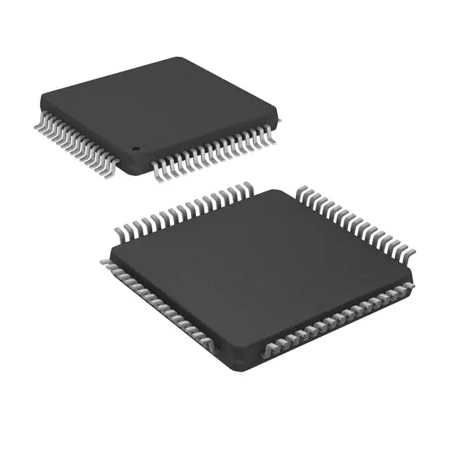


 工商网监
湘ICP备2023018690号
工商网监
湘ICP备2023018690号