Sample &
Buy
Product
Folder
Support &
Community
Tools &
Software
Technical
Documents
ADS4222, ADS4225, ADS4226
ADS4242, ADS4245, ADS4246
SBAS533D – MARCH 2011 – REVISED DECEMBER 2015
ADS42xx Dual-Channel, 14-/12-Bit, 160/125/65 MSPS Ultralow-Power ADC
1 Features
2 Applications
•
•
•
•
1
•
•
•
•
•
•
•
Ultralow Power With Single 1.8-V Supply, CMOS
Output:
– 183 mW Total Power at 65 MSPS
– 277 mW Total Power at 125 MSPS
– 332 mW Total Power at 160 MSPS
High Dynamic Performance:
– 88-dBc SFDR at 170 MHz
– 71.4-dBFS SNR at 170 MHz
Crosstalk: > 90 dB at 185 MHz
Programmable Gain up to 6 dB for SNR/SFDR
Trade-off
DC Offset Correction
Output Interface Options:
– 1.8-V parallel CMOS Interface
– Double Data Rate (DDR) LVDS With
Programmable swing:
– Standard Swing: 350 mV
– Low Swing: 200 mV
Supports Low Input Clock Amplitude Down to 200
mVPP
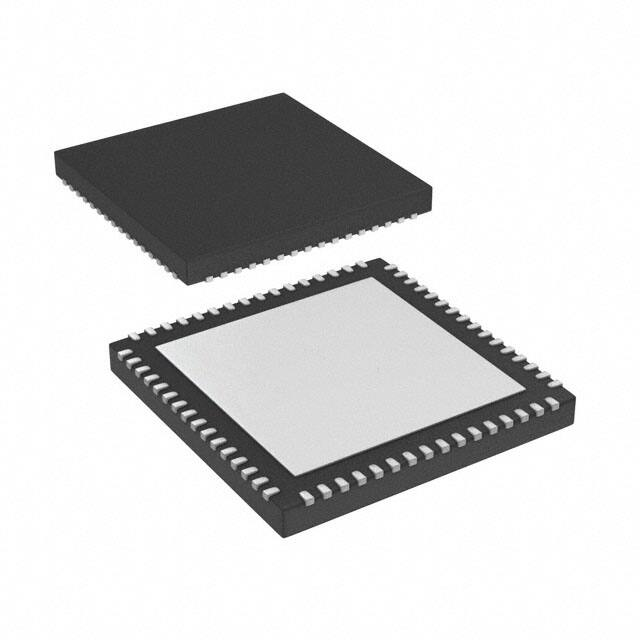
Package: VQFN-64 (9.00 mm × 9.00 mm)
Wireless Communications Infrastructure
Software-Defined Radio
Power Amplifier Linearization
3 Description
The ADS424x and ADS422x family of devices are
low-speed variants of the ADS42xx ultralow-power
family of dual-channel, 14-bit/12-bit analog-to-digital
converters (ADCs). Innovative design techniques are
used to achieve high-dynamic performance, while
consuming extremely low power with 1.8-V supply.
This topology makes the ADS424x/422x well-suited
for multi-carrier, wide-bandwidth communications
applications.
Device Information(1)
PART NUMBER
PACKAGE
BODY SIZE (NOM)
ADS4222
ADS4225
ADS4226
VQFN (48)
ADS4242
9.00 mm × 9.00 mm
ADS4245
ADS4246
(1) For all available packages, see the orderable addendum at
the end of the data sheet.
ADS4222/25/26/42/45/46 Block Diagram
AVDD
AGND
DRVDD
DRGND
LVDS Interface
DA0P
DA0M
DA2P
DA2M
DA4P
INP_A
Sampling
Circuit
INM_A
Digital and
DDR
Serializer
14-Bit
ADC
DA4M
DA6P
DA6M
DA8P
DA8M
DA10P
DA10M
DA12P
DA12M
CLKP
Output
Clock Buffer
CLOCKGEN
CLKM
CLKOUTP
CLKOUTM
DB0P
DB0M
DB2P
DB2M
DB4P
INP_B
Sampling
Circuit
INM_B
Digital and
DDR
Serializer
14-Bit
ADC
DB4M
DB6P
DB6M
DB8P
DB8M
DB10P
DB10M
DB12P
DB12M
CTRL1
CTRL3
SDOUT
CTRL2
SCLK
RESET
ADS424x
SEN
Reference
VCM
SDATA
Control
Interface
1
An IMPORTANT NOTICE at the end of this data sheet addresses availability, warranty, changes, use in safety-critical applications,
intellectual property matters and other important disclaimers. PRODUCTION DATA.
�ADS4222, ADS4225, ADS4226
ADS4242, ADS4245, ADS4246
SBAS533D – MARCH 2011 – REVISED DECEMBER 2015
www.ti.com
Table of Contents
1
2
3
4
5
6
7
8
Features .................................................................. 1
Applications ........................................................... 1
Description ............................................................. 1
Revision History..................................................... 2
Description (continued)......................................... 3
ADS424x/422x Family Comparison...................... 4
Pin Configuration and Functions ......................... 5
Specifications....................................................... 10
8.1
8.2
8.3
8.4
8.5
Absolute Maximum Ratings ....................................
ESD Ratings............................................................
Recommended Operating Conditions.....................
Thermal Information ................................................
Electrical Characteristics: ADS4246, ADS4245,
ADS4242..................................................................
8.6 Electrical Characteristics: ADS4226, ADS4225,
ADS4222..................................................................
8.7 Electrical Characteristics: General ..........................
8.8 Digital Characteristics .............................................
8.9 Timing Requirements: LVDS and CMOS Modes....
8.10 Serial Interface Timing Characteristics .................
8.11 Reset Timing (Only When Serial Interface Is
Used)........................................................................
8.12 Typical Characteristics ..........................................
9
10
10
11
11
9.2
9.3
9.4
9.5
9.6
Functional Block Diagrams .....................................
Feature Description.................................................
Device Functional Modes........................................
Programming...........................................................
Register Maps .........................................................
49
51
57
58
67
10 Application and Implementation........................ 79
10.1 Application Information.......................................... 79
10.2 Typical Application ............................................... 80
11 Power Supply Recommendations ..................... 83
11.1 Sharing DRVDD and AVDD Supplies ................... 83
11.2 Using DC/DC Power Supplies .............................. 83
11.3 Power Supply Bypassing ...................................... 83
12 Layout................................................................... 83
12
12.1 Layout Guidelines ................................................. 83
12.2 Layout Example .................................................... 84
15
18
19
19
20
13 Device and Documentation Support ................. 85
20
25
Detailed Description ............................................ 49
9.1 Overview ................................................................. 49
13.1
13.2
13.3
13.4
13.5
13.6
13.7
Device Support ....................................................
Documentation Support .......................................
Related Links ........................................................
Community Resources..........................................
Trademarks ...........................................................
Electrostatic Discharge Caution ............................
Glossary ................................................................
85
86
87
87
87
87
87
14 Mechanical, Packaging, and Orderable
Information ........................................................... 87
4 Revision History
NOTE: Page numbers for previous revisions may differ from page numbers in the current version.
Changes from Revision C (March 2011) to Revision D
•
Page
Added ESD Ratings table, Feature Description section, Device Functional Modes, Application and Implementation
section, Power Supply Recommendations section, Layout section, Device and Documentation Support section, and
Mechanical, Packaging, and Orderable Information section. ................................................................................................ 1
Changes from Revision B (May 2011) to Revision C
Page
•
Changed device status from Mixed Status to Production Data.............................................................................................. 1
•
Changed 125MSPS sub-bullet of first Features bullet ........................................................................................................... 1
•
Changed sub-bullets of second Features bullet ..................................................................................................................... 1
•
Changed description of pin 64 in Pin Descriptions: LVDS Mode table .................................................................................. 7
•
Changed description of pin 64 in Pin Descriptions: CMOS Mode table............................................................................... 10
•
Changed ADS4246 fIN = 170 MHz Worst spur typical spcification in the ADS4246/ADS4245/ADS4242 Electrical
Characteristics table ............................................................................................................................................................. 14
•
Added ADS4225/ADS4222 fIN = 70 MHz SNR, SINAD, SFDR, THD, HD2, HD3, and Worst spur minimum and
typical spcifications in the ADS4226/ADS4225/ADS4222 Electrical Characteristics table .................................................. 15
•
Added ADS4225/ADS4222 DNL minimum and maximum spcifications in the ADS4226/ADS4225/ADS4222
Electrical Characteristics table ............................................................................................................................................. 17
•
Added ADS4225/ADS4222 INL maximum spcifications in the ADS4226/ADS4225/ADS4222 Electrical
Characteristics table ............................................................................................................................................................. 17
•
Changed ADS4242/ADS4222 Power Supply, Digital power LVDS interface typical specification in Electrical
Characteristics: General table .............................................................................................................................................. 18
2
Submit Documentation Feedback
Copyright © 2011–2015, Texas Instruments Incorporated
Product Folder Links: ADS4222 ADS4225 ADS4226 ADS4242 ADS4245 ADS4246
�ADS4222, ADS4225, ADS4226
ADS4242, ADS4245, ADS4246
www.ti.com
SBAS533D – MARCH 2011 – REVISED DECEMBER 2015
•
Changed ADS4245/ADS4225 Power Supply, Digital power CMOS interface typical specification in Electrical
Characteristics: General table .............................................................................................................................................. 18
•
Moved High-Performance Modes into separate table .......................................................................................................... 21
•
Changed description of READOUT disabled in Serial Register Readout section................................................................ 60
•
Updated Figure 152.............................................................................................................................................................. 61
•
Changed READOUT desciption in Register Address 00h section ....................................................................................... 68
•
Changed CLKOUT FALL POSN and CLKOUT RISE POSN description in Register Address 42h section ........................ 73
Changes from Revision A (May 2011) to Revision B
Page
•
Changed sub-bullets of first Features bullet........................................................................................................................... 1
•
Updated description of NC pin in LVDS Pin Descriptions table ............................................................................................. 7
•
Updated description of NC pin in CMOS Pin Descriptions table.......................................................................................... 10
•
Changed ENOB, DNL, and INL test conditions in the Electrical Characteristics: ADS4246/ADS4245/ADS4242 table ..... 14
•
Deleted INL minimum specifications from Electrical Characteristics: ADS4246/ADS4245/ADS4242 table ........................ 14
•
Changed INL maximum specifications in the Electrical Characteristics: ADS4246/ADS4245/ADS4242 table.................... 14
•
Changed ENOB, DNL, and INL test conditions in the Electrical Characteristics: ADS4226/ADS4225/ADS4222 table ..... 17
•
Changed ADS4226 INL maximum specification in the Electrical Characteristics: ADS4226/ADS4225/ADS4222 table ..... 17
•
Changed Power Supply, IDRVDD and Digital power CMOS interface rows in the Electrical Characteristics: General
table ...................................................................................................................................................................................... 18
•
Updated Figure 16................................................................................................................................................................ 25
•
Updated Figure 18................................................................................................................................................................ 26
•
Updated Figure 37 and Figure 38 ........................................................................................................................................ 29
•
Updated Figure 39 and Figure 40 ........................................................................................................................................ 29
•
Updated Figure 58 and Figure 59 ........................................................................................................................................ 33
•
Updated Figure 60 and Figure 61 ........................................................................................................................................ 34
•
Updated Figure 79 and Figure 80 ........................................................................................................................................ 37
•
Updated Figure 81 and Figure 82 ........................................................................................................................................ 37
•
Updated Figure 96................................................................................................................................................................ 40
•
Updated Figure 97 and SBAS533graph8650 ....................................................................................................................... 40
•
Updated Figure 115.............................................................................................................................................................. 43
•
Updated Figure 127.............................................................................................................................................................. 46
•
Changed title of Figure 128 .................................................................................................................................................. 46
•
Updated ADS424x/422x Family Pins section in Table 4 ...................................................................................................... 51
•
Changed 111110 and 001111 LVDS SWING description in Register Address 01h ............................................................ 68
5 Description (continued)
The ADS424x/422x have gain options that can be used to improve SFDR performance at lower full-scale input
ranges. These devices include a dc offset correction loop that can be used to cancel the ADC offset. Both DDR
(double data rate) LVDS and parallel CMOS digital output interfaces are available in a compact VQFN-64
package.
The devices include internal references while the traditional reference pins and associated decoupling capacitors
have been eliminated. All devices are specified over the industrial temperature range (–40°C to 85°C).
Copyright © 2011–2015, Texas Instruments Incorporated
Submit Documentation Feedback
Product Folder Links: ADS4222 ADS4225 ADS4226 ADS4242 ADS4245 ADS4246
3
�ADS4222, ADS4225, ADS4226
ADS4242, ADS4245, ADS4246
SBAS533D – MARCH 2011 – REVISED DECEMBER 2015
www.ti.com
6 ADS424x/422x Family Comparison
(1)
4
DEVICE FAMILY (1)
250 MSPS
160 MSPS
125 MSPS
65 MSPS
ADS424x
14-bit family
ADS4249
ADS4246
ADS4245
ADS4242
ADS422x
12-bit family
ADS4229
ADS4226
ADS4225
ADS4222
See Table 4 for details on migrating from the ADS62P49 family.
Submit Documentation Feedback
Copyright © 2011–2015, Texas Instruments Incorporated
Product Folder Links: ADS4222 ADS4225 ADS4226 ADS4242 ADS4245 ADS4246
�ADS4222, ADS4225, ADS4226
ADS4242, ADS4245, ADS4246
www.ti.com
SBAS533D – MARCH 2011 – REVISED DECEMBER 2015
7 Pin Configuration and Functions
49 DRGND
50 DA8M
51 DA8P
52 DA10M
53 DA10P
54 DA12M
55 DA12P
56 CLKOUTM
57 CLKOUTP
58 NC
59 NC
60 DB0M
61 DB0P
62 DB2M
63 DB2P
64 SDOUT
ADS4246, ADS4245, and ADS4242 RGC Package
64-Pin VQFN With Exposed Thermal Pad
LVDS Mode - Top View
DRVDD
1
48 DRVDD
DB4M
2
47 DA6P
DB4P
3
46 DA6M
DB6M
4
45 DA4P
DB6P
5
42 DA4M
DB8M
6
43 DA2P
42 DA2M
DB8P
7
DB10M
8
DB10P
9
41 DA0P
Thermal Pad
(Connected to DRGND)
40 DA0M
DB12M 10
39 NC
DB12P 11
38 NC
RESET 12
37 CTRL3
SCLK 13
36 CTRL2
SDATA 14
35 CTRL1
AGND 32
AGND 31
INM_A 30
INP_A 29
AGND 28
AGND 27
CLKM 26
CLKP 25
VCM 23
AGND 24
AVDD 22
AGND 21
INP_B 19
Copyright © 2011–2015, Texas Instruments Incorporated
INM_B 20
33 AVDD
AGND 17
34 AVDD
AVDD 16
AGND 18
SEN 15
Submit Documentation Feedback
Product Folder Links: ADS4222 ADS4225 ADS4226 ADS4242 ADS4245 ADS4246
5
�ADS4222, ADS4225, ADS4226
ADS4242, ADS4245, ADS4246
SBAS533D – MARCH 2011 – REVISED DECEMBER 2015
www.ti.com
49 DRGND
50 DA6M
51 DA6P
52 DA8M
53 DA8P
54 DA10M
55 DA10P
56 CLKOUTM
57 CLKOUTP
58 NC
59 NC
60 NC
61 NC
62 DB0M
63 DB0P
64 SDOUT
ADS4226, ADS4225, and ADS4222 RGC Package
64-Pin VQFN With Exposed Thermal Pad
LVDS Mode - Top View
DRVDD
1
48 DRVDD
DB2M
2
47 DA4P
DB2P
3
46 DA4M
DB4M
4
45 DA2P
DB4P
5
42 DA2M
DB6M
6
43 DA0P
42 DA0M
DB6P
7
DB8M
8
DB8P
9
41 NC
Thermal Pad
(Connected to DRGND)
40 NC
DB10M 10
39 NC
DB10P 11
38 NC
RESET 12
37 CTRL3
SCLK 13
36 CTRL2
SDATA 14
35 CTRL1
AGND 32
AGND 31
INM_A 30
INP_A 29
AGND 28
AGND 27
CLKM 26
CLKP 25
VCM 23
AGND 24
AVDD 22
AGND 21
INP_B 19
INM_B 20
33 AVDD
AGND 17
34 AVDD
AVDD 16
AGND 18
SEN 15
Pin Functions – LVDS Mode
PIN
I/O
DESCRIPTION
NAME
NO.
AGND
17, 18, 21, 24, 27, 28,
31, 32
Input
Analog ground
AVDD
16, 22, 33, 34
Input
Analog power supply
CLKM
26
Input
Differential clock negative input
CLKOUTM
56
Output
Differential output clock, complement
CLKOUTP
57
Output
Differential output clock, true
CLKP
25
Input
Differential clock positive input
CTRL1
35
Input
Digital control input pins. Together, they control the various power-down modes.
CTRL2
36
Input
Digital control input pins. Together, they control the various power-down modes.
CTRL3
37
Input
Digital control input pins. Together, they control the various power-down modes.
DA0P, DA0M
Refer to pinout
drawings
Output
Channel A differential output data pair, D0 and D1 multiplexed
DA2P, DA2M
Refer to pinout
drawings
Output
Channel A differential output data D2 and D3 multiplexed
DA4P, DA4M
Refer to pinout
drawings
Output
Channel A differential output data D4 and D5 multiplexed
DA6P, DA6M
Refer to pinout
drawings
Output
Channel A differential output data D6 and D7 multiplexed
DA8P, DA8M
Refer to pinout
drawings
Output
Channel A differential output data D8 and D9 multiplexed
DA10P, DA10M
Refer to pinout
drawings
Output
Channel A differential output data D10 and D11 multiplexed
6
Submit Documentation Feedback
Copyright © 2011–2015, Texas Instruments Incorporated
Product Folder Links: ADS4222 ADS4225 ADS4226 ADS4242 ADS4245 ADS4246
�ADS4222, ADS4225, ADS4226
ADS4242, ADS4245, ADS4246
www.ti.com
SBAS533D – MARCH 2011 – REVISED DECEMBER 2015
Pin Functions – LVDS Mode (continued)
PIN
I/O
DESCRIPTION
NAME
NO.
DA12P, DA12M
Refer to pinout
drawings
Output
Channel A differential output data D12 and D13 multiplexed (ADS424x only)
DB0P, DB0M
Refer to pinout
drawings
Output
Channel B differential output data pair, D0 and D1 multiplexed
DB2P, DB2M
Refer to pinout
drawings
Output
Channel B differential output data D2 and D3 multiplexed
DB4P, DB4M
Refer to pinout
drawings
Output
Channel B differential output data D4 and D5 multiplexed
DB6P, DB6M
Refer to pinout
drawings
Output
Channel B differential output data D6 and D7 multiplexed
DB8P, DB8M
Refer to pinout
drawings
Output
Channel B differential output data D8 and D9 multiplexed
DB10P, DB10M
Refer to pinout
drawings
Output
Channel B differential output data D10 and D11 multiplexed
DB12P, DB12M
Refer to pinout
drawings
Output
Channel B differential output data D12 and D13 multiplexed (ADS424x only)
DRGND
49, PAD
Input
Output buffer ground
DRVDD
1, 48
Input
Output buffer supply
INM_A
30
Input
Differential analog negative input, channel A
INM_B
20
Input
Differential analog negative input, channel B
INP_A
29
Input
Differential analog positive input, channel A
INP_B
19
Input
Differential analog positive input, channel B
NC
Refer to Figure 28,
Figure 29, and
Figure 45
—
Do not connect, must be floated
RESET
12
Input
Serial interface RESET input.
When using the serial interface mode, the internal registers must be initialized through a
hardware RESET by applying a high pulse on this pin or by using the software reset option;
refer to the Serial Interface Configuration section.
In parallel interface mode, the RESET pin must be permanently tied high. SCLK and SEN
are used as parallel control pins in this mode. This pin has an internal 150-kΩ pulldown
resistor.
SCLK
13
Input
This pin functions as a serial interface clock input when RESET is low. It controls the lowspeed mode selection when RESET is tied high; see Table 9 for detailed information. This
pin has an internal 150-kΩ pulldown resistor.
SDATA
14
Input
Serial interface data input; this pin has an internal 150-kΩ pulldown resistor.
SDOUT
64
Output
SEN
15
Input
VCM
23
Output
Copyright © 2011–2015, Texas Instruments Incorporated
This pin functions as a serial interface register readout when the READOUT bit is enabled.
When READOUT = 0, this pin is in high-impedance state.
This pin functions as a serial interface enable input when RESET is low. It controls the
output interface and data format selection when RESET is tied high; see Table 10 for
detailed information. This pin has an internal 150-kΩ pullup resistor to AVDD.
This pin outputs the common-mode voltage (0.95 V) that can be used externally to bias the
analog input pins
Submit Documentation Feedback
Product Folder Links: ADS4222 ADS4225 ADS4226 ADS4242 ADS4245 ADS4246
7
�ADS4222, ADS4225, ADS4226
ADS4242, ADS4245, ADS4246
SBAS533D – MARCH 2011 – REVISED DECEMBER 2015
www.ti.com
49 DRGND
50 DA8
51 DA9
52 DA10
53 DA11
54 DA12
55 DA13
56 UNUSED
57 CLKOUT
58 NC
59 NC
60 DB0
61 DB1
62 DB2
DRVDD
1
48 DRVDD
DB4
2
47 DA7
DB5
3
46 DA6
DB6
4
45 DA5
DB7
5
42 DA4
DB8
6
43 DA3
DB9
7
42 DA2
DB10
8
DB11
9
41 DA1
Thermal Pad
(Connected to DRGND)
40 DA0
DB12 10
39 NC
DB13 11
38 NC
RESET 12
37 CTRL3
SCLK 13
36 CTRL2
SDATA 14
35 CTRL1
Submit Documentation Feedback
AGND 32
AGND 31
INM_A 30
INP_A 29
AGND 28
AGND 27
CLKM 26
CLKP 25
VCM 23
AGND 24
AVDD 22
AGND 21
33 AVDD
INP_B 19
AVDD 16
INM_B 20
34 AVDD
AGND 18
SEN 15
AGND 17
8
63 DB3
64 SDOUT
ADS4246, ADS4245, and ADS4242 RGC Package
64-Pin VQFN With Exposed Thermal Pad
CMOS Mode - Top View
Copyright © 2011–2015, Texas Instruments Incorporated
Product Folder Links: ADS4222 ADS4225 ADS4226 ADS4242 ADS4245 ADS4246
�ADS4222, ADS4225, ADS4226
ADS4242, ADS4245, ADS4246
www.ti.com
SBAS533D – MARCH 2011 – REVISED DECEMBER 2015
49 DRGND
50 DA6
51 DA7
52 DA8
53 DA9
54 DA10
55 DA11
56 UNUSED
57 CLKOUT
58 NC
59 NC
60 NC
61 NC
62 DB0
63 DB1
64 SDOUT
ADS4226, ADS4225, and ADS4222 RGC Package
64-Pin VQFN With Exposed Thermal Pad
CMOS Mode - Top View
DRVDD
1
48 DRVDD
DB2
2
47 DA5
DB3
3
46 DA4
DB4
4
45 DA3
DB5
5
42 DA2
DB6
6
43 DA1
DB7
7
42 DA0
DB8
8
DB9
9
41 NC
Thermal Pad
(Connected to DRGND)
40 NC
DB10 10
39 NC
DB11 11
38 NC
RESET 12
37 CTRL3
SCLK 13
36 CTRL2
SDATA 14
35 CTRL1
AGND 32
AGND 31
INM_A 30
INP_A 29
AGND 28
AGND 27
CLKM 26
CLKP 25
VCM 23
AGND 24
AVDD 22
AGND 21
INP_B 19
33 AVDD
INM_B 20
AVDD 16
AGND 17
34 AVDD
AGND 18
SEN 15
Pin Functions – CMOS Mode
PIN
I/O
DESCRIPTION
NAME
NO.
AGND
17, 18, 21, 24, 27, 28,
31, 32
Input
Analog ground
AVDD
16, 22, 33, 34
Input
Analog power supply
CLKM
26
Input
Differential clock negative input
CLKOUT
57
Output
CLKP
25
Input
Differential clock positive input
CTRL1
35
Input
Digital control input pins. Together, they control various power-down modes.
CTRL2
36
Input
Digital control input pins. Together, they control various power-down modes.
CTRL3
37
Input
Digital control input pins. Together, they control various power-down modes.
DA0 to DA11
Refer to pinout
drawings
Output
Channel A ADC output data bits, CMOS levels
DA12 to DA13
Refer to pinout
drawings
Output
Channel A ADC output data bits, CMOS levels (ADS424x only)
DB0 to DB11
Refer to pinout
drawings
Output
Channel B ADC output data bits, CMOS levels
DB12 to DB13
Refer to pinout
drawings
Output
Channel B ADC output data bits, CMOS levels (ADS424x only)
DRGND
49, PAD
Input
Output buffer ground
DRVDD
1, 48
Input
Output buffer supply
INM_A
30
Input
Differential analog negative input, channel A
INM_B
20
Input
Differential analog negative input, channel B
INP_A
29
Input
Differential analog positive input, channel A
Copyright © 2011–2015, Texas Instruments Incorporated
CMOS output clock
Submit Documentation Feedback
Product Folder Links: ADS4222 ADS4225 ADS4226 ADS4242 ADS4245 ADS4246
9
�ADS4222, ADS4225, ADS4226
ADS4242, ADS4245, ADS4246
SBAS533D – MARCH 2011 – REVISED DECEMBER 2015
www.ti.com
Pin Functions – CMOS Mode (continued)
PIN
I/O
NAME
NO.
INP_B
19
Input
NC
—
—
DESCRIPTION
Differential analog positive input, channel B
Do not connect, must be floated
RESET
12
Input
Serial interface RESET input.
When using the serial interface mode, the internal registers must be initialized through a
hardware RESET by applying a high pulse on this pin or by using the software reset option;
refer to the Serial Interface Configuration section.
In parallel interface mode, the RESET pin must be permanently tied high. SDATA and SEN are
used as parallel control pins in this mode. This pin has an internal 150-kΩ pulldown resistor.
SCLK
13
Input
This pin functions as a serial interface clock input when RESET is low. It controls the lowspeed mode when RESET is tied high; see Table 9 for detailed information. This pin has an
internal 150-kΩ pulldown resistor.
SDATA
14
Input
Serial interface data input; this pin has an internal 150-kΩ pulldown resistor.
SDOUT
64
Output
SEN
15
Input
UNUSED
56
—
VCM
23
Output
This pin functions as a serial interface register readout when the READOUT bit is enabled.
When READOUT = 0, this pin is in high-impedance state.
This pin functions as a serial interface enable input when RESET is low. It controls the output
interface and data format selection when RESET is tied high; see Table 10 for detailed
information. This pin has an internal 150-kΩ pullup resistor to AVDD.
This pin is not used in the CMOS interface
This pin outputs the common-mode voltage (0.95 V) that can be used externally to bias the
analog input pins
8 Specifications
8.1 Absolute Maximum Ratings
over operating free-air temperature range (unless otherwise noted) (1)
MIN
MAX
UNIT
Supply voltage range, AVDD
–0.3
2.1
V
Supply voltage range, DRVDD
–0.3
2.1
V
Voltage between AGND and DRGND
–0.3
0.3
V
Voltage between AVDD to DRVDD (when AVDD leads DRVDD)
–2.4
2.4
V
Voltage between DRVDD to AVDD (when DRVDD leads AVDD)
–2.4
2.4
V
INP_A, INM_A, INP_B, INM_B
–0.3
Minimum
(1.9, AVDD + 0.3)
V
CLKP, CLKM (2)
–0.3
AVDD + 0.3
V
RESET, SCLK, SDATA, SEN,
CTRL1, CTRL2, CTRL3
–0.3
3.9
V
Voltage applied to input pins
Operating free-air temperature range, TA
–40
Operating junction temperature range, TJ
Storage temperature range, Tstg
(1)
(2)
–65
85
°C
125
°C
150
°C
Stresses beyond those listed under Absolute Maximum Ratings may cause permanent damage to the device. These are stress ratings
only, which do not imply functional operation of the device at these or any other conditions beyond those indicated under Recommended
Operating Conditions. Exposure to absolute-maximum-rated conditions for extended periods may affect device reliability.
When AVDD is turned off, it is recommended to switch off the input clock (or ensure the voltage on CLKP, CLKM is less than |0.3 V|).
This configuration prevents the ESD protection diodes at the clock input pins from turning on.
8.2 ESD Ratings
VALUE
V(ESD)
(1)
(2)
10
Electrostatic discharge
Human-body model (HBM), per ANSI/ESDA/JEDEC JS-001 (1)
±2000
Charged-device model (CDM), per JEDEC specification JESD22C101 (2)
±500
UNIT
V
JEDEC document JEP155 states that 500-V HBM allows safe manufacturing with a standard ESD control process.
JEDEC document JEP157 states that 250-V CDM allows safe manufacturing with a standard ESD control process.
Submit Documentation Feedback
Copyright © 2011–2015, Texas Instruments Incorporated
Product Folder Links: ADS4222 ADS4225 ADS4226 ADS4242 ADS4245 ADS4246
�ADS4222, ADS4225, ADS4226
ADS4242, ADS4245, ADS4246
www.ti.com
SBAS533D – MARCH 2011 – REVISED DECEMBER 2015
8.3 Recommended Operating Conditions
Over operating free-air temperature range, unless otherwise noted.
MIN
NOM
MAX
UNIT
Analog supply voltage, AVDD
1.7
1.8
1.9
V
Digital supply voltage, DRVDD
1.7
1.8
1.9
V
SUPPLIES
ANALOG INPUTS
Differential input voltage range
2
Input common-mode voltage
VPP
VCM ± 0.05
V
Maximum analog input frequency with 2 VPP input amplitude (1)
400
MHz
Maximum analog input frequency with 1 VPP input amplitude (1)
600
MHz
CLOCK INPUT
Input clock sample rate (ADS4242/ADS4222)
Input clock sample rate (ADS4245/ADS4225)
Input clock sample rate (ADS4246/ADS4226)
Input clock amplitude differential
(VCLKP – VCLKM)
Low-speed mode enabled (by default after reset)
Low-speed mode enabled
1
(2)
Low-speed mode disabled (2) (by default after reset)
Low-speed mode enabled (2)
65
MSPS
1
80
MSPS
80
125
1
80
MSPS
Low-speed mode disabled (2) (by default after reset)
80
160
MSPS
Sine wave, ac-coupled
0.2
1.5
VPP
LVPECL, ac-coupled
1.6
VPP
LVDS, ac-coupled
0.7
VPP
LVCMOS, single-ended, ac-coupled
1.5
V
INPUT CLOCK DUTY CYCLE
Low-speed mode disabled
35%
50%
65%
Low-speed mode enabled
40%
50%
60%
DIGITAL OUTPUTS
Maximum external load capacitance from each output pin to DRGND, CLOAD
Differential load resistance between the LVDS output pairs (LVDS mode), RLOAD
Operating free-air temperature, TA
(1)
(2)
5
pF
100
Ω
–40
85
°C
See the Application InformationA section in the Application Information.
See the Serial Interface Configuration section for details on programming the low-speed mode.
8.4 Thermal Information
ADS42xx
THERMAL METRIC (1)
RGC (VQFN)
UNIT
64 PINS
RθJA
Junction-to-ambient thermal resistance
23.9
°C/W
RθJC(top)
Junction-to-case (top) thermal resistance
10.9
°C/W
RθJB
Junction-to-board thermal resistance
4.3
°C/W
ψJT
Junction-to-top characterization parameter
0.1
°C/W
ψJB
Junction-to-board characterization parameter
4.4
°C/W
RθJC(bot)
Junction-to-case (bottom) thermal resistance
0.6
°C/W
(1)
For more information about traditional and new thermal metrics, see the Semiconductor and IC Package Thermal Metrics application
report (SPRA953).
Copyright © 2011–2015, Texas Instruments Incorporated
Submit Documentation Feedback
Product Folder Links: ADS4222 ADS4225 ADS4226 ADS4242 ADS4245 ADS4246
11
�ADS4222, ADS4225, ADS4226
ADS4242, ADS4245, ADS4246
SBAS533D – MARCH 2011 – REVISED DECEMBER 2015
www.ti.com
8.5 Electrical Characteristics: ADS4246, ADS4245, ADS4242
Typical values are at 25°C, AVDD = 1.8 V, DRVDD = 1.8 V, 50% clock duty cycle, –1 dBFS differential analog input, LVDS
interface, and 0-dB gain, unless otherwise noted. Minimum and maximum values are across the full temperature range: TMIN
= –40°C to TMAX = 85°C, AVDD = 1.8 V, and DRVDD = 1.8 V.
PARAMETER
TEST CONDITIONS
MIN
TYP
Resolution
14
fIN = 20 MHz
ADS4246 (160 MSPS)
72.8
ADS4245 (125 MSPS)
73.4
ADS4242 (65 MSPS)
73.6
ADS4246 (160 MSPS)
fIN = 70 MHz
ADS4245 (125 MSPS)
ADS4242 (65 MSPS)
Signal-to-noise ratio
SNR
fIN = 100 MHz
fIN = 300 MHz
fIN = 20 MHz
72.9
69.5
72.5
72.2
ADS4245 (125 MSPS)
72.6
ADS4242 (65 MSPS)
72.3
69
71.4
ADS4242 (65 MSPS)
70.4
ADS4246 (160 MSPS)
69.4
ADS4245 (125 MSPS)
69.3
ADS4242 (65 MSPS)
69.4
ADS4246 (160 MSPS)
72.6
ADS4245 (125 MSPS)
73.2
ADS4242 (65 MSPS)
73.5
ADS4245 (125 MSPS)
ADS4242 (65 MSPS)
SINAD
fIN = 100 MHz
fIN = 300 MHz
fIN = 20 MHz
72.6
68.5
72.3
71.7
ADS4245 (125 MSPS)
72.3
ADS4242 (65 MSPS)
72.1
67.5
Spurious-free dynamic range
SFDR
fIN = 100 MHz
71.2
ADS4242 (65 MSPS)
70.2
ADS4246 (160 MSPS)
68
ADS4245 (125 MSPS)
68.5
ADS4242 (65 MSPS)
68.2
ADS4246 (160 MSPS)
86
ADS4245 (125 MSPS)
88
ADS4242 (65 MSPS)
91
fIN = 300 MHz
12
Submit Documentation Feedback
dBFS
dBFS
dBFS
dBFS
dBFS
dBFS
dBFS
dBFS
dBc
84
ADS4245 (125 MSPS)
73.5
86
ADS4242 (65 MSPS)
73.5
88
ADS4246 (160 MSPS)
82
ADS4245 (125 MSPS)
85
ADS4242 (65 MSPS)
87
ADS4246 (160 MSPS)
fIN = 170 MHz
dBFS
70.8
ADS4245 (125 MSPS)
ADS4246 (160 MSPS)
fIN = 70 MHz
dBFS
72.1
69
ADS4246 (160 MSPS)
ADS4246 (160 MSPS)
fIN = 170 MHz
Bits
71.2
ADS4245 (125 MSPS)
ADS4246 (160 MSPS)
fIN = 70 MHz
UNIT
72.5
70
ADS4246 (160 MSPS)
ADS4246 (160 MSPS)
fIN = 170 MHz
Signal-to-noise and
distortion ratio
MAX
72
dBc
dBc
82
ADS4245 (125 MSPS)
88
ADS4242 (65 MSPS)
85
ADS4246 (160 MSPS)
78
ADS4245 (125 MSPS)
78
ADS4242 (65 MSPS)
74
dBc
dBc
Copyright © 2011–2015, Texas Instruments Incorporated
Product Folder Links: ADS4222 ADS4225 ADS4226 ADS4242 ADS4245 ADS4246
�ADS4222, ADS4225, ADS4226
ADS4242, ADS4245, ADS4246
www.ti.com
SBAS533D – MARCH 2011 – REVISED DECEMBER 2015
Electrical Characteristics: ADS4246, ADS4245, ADS4242 (continued)
Typical values are at 25°C, AVDD = 1.8 V, DRVDD = 1.8 V, 50% clock duty cycle, –1 dBFS differential analog input, LVDS
interface, and 0-dB gain, unless otherwise noted. Minimum and maximum values are across the full temperature range: TMIN
= –40°C to TMAX = 85°C, AVDD = 1.8 V, and DRVDD = 1.8 V.
PARAMETER
TEST CONDITIONS
fIN = 20 MHz
MIN
84
ADS4245 (125 MSPS)
86
ADS4242 (65 MSPS)
88
ADS4246 (160 MSPS)
fIN = 70 MHz
Total harmonic distortion
THD
fIN = 100 MHz
fIN = 300 MHz
fIN = 20 MHz
72
84
ADS4242 (65 MSPS)
72
85
ADS4246 (160 MSPS)
81
ADS4245 (125 MSPS)
83
ADS4242 (65 MSPS)
85
70
Second-harmonic distortion
HD2
fIN = 100 MHz
84
ADS4242 (65 MSPS)
82
ADS4246 (160 MSPS)
76
ADS4245 (125 MSPS)
75
ADS4242 (65 MSPS)
73
ADS4246 (160 MSPS)
86
ADS4245 (125 MSPS)
88
ADS4242 (65 MSPS)
91
fIN = 300 MHz
fIN = 20 MHz
73.5
86
ADS4242 (65 MSPS)
73.5
88
ADS4246 (160 MSPS)
82
ADS4245 (125 MSPS)
85
ADS4242 (65 MSPS)
87
72
Third-harmonic distortion
HD3
fIN = 100 MHz
88
ADS4242 (65 MSPS)
85
ADS4246 (160 MSPS)
78
ADS4245 (125 MSPS)
78
ADS4242 (65 MSPS)
74
ADS4246 (160 MSPS)
92
ADS4245 (125 MSPS)
93
ADS4242 (65 MSPS)
95
fIN = 300 MHz
Copyright © 2011–2015, Texas Instruments Incorporated
dBc
dBc
dBc
dBc
dBc
dBc
dBc
dBc
dBc
86
ADS4245 (125 MSPS)
73.5
89
ADS4242 (65 MSPS)
73.5
90
ADS4246 (160 MSPS)
93
ADS4245 (125 MSPS)
89
ADS4242 (65 MSPS)
96
ADS4246 (160 MSPS)
fIN = 170 MHz
dBc
82
ADS4245 (125 MSPS)
ADS4246 (160 MSPS)
fIN = 70 MHz
dBc
84
ADS4245 (125 MSPS)
ADS4246 (160 MSPS)
fIN = 170 MHz
UNIT
80
ADS4245 (125 MSPS)
ADS4246 (160 MSPS)
fIN = 70 MHz
MAX
81
ADS4245 (125 MSPS)
ADS4246 (160 MSPS)
fIN = 170 MHz
TYP
ADS4246 (160 MSPS)
72
dBc
94
ADS4245 (125 MSPS)
90
ADS4242 (65 MSPS)
87
ADS4246 (160 MSPS)
80
ADS4245 (125 MSPS)
81
ADS4242 (65 MSPS)
81
Submit Documentation Feedback
Product Folder Links: ADS4222 ADS4225 ADS4226 ADS4242 ADS4245 ADS4246
dBc
dBc
dBc
13
�ADS4222, ADS4225, ADS4226
ADS4242, ADS4245, ADS4246
SBAS533D – MARCH 2011 – REVISED DECEMBER 2015
www.ti.com
Electrical Characteristics: ADS4246, ADS4245, ADS4242 (continued)
Typical values are at 25°C, AVDD = 1.8 V, DRVDD = 1.8 V, 50% clock duty cycle, –1 dBFS differential analog input, LVDS
interface, and 0-dB gain, unless otherwise noted. Minimum and maximum values are across the full temperature range: TMIN
= –40°C to TMAX = 85°C, AVDD = 1.8 V, and DRVDD = 1.8 V.
PARAMETER
TEST CONDITIONS
fIN = 20 MHz
MIN
90
ADS4245 (125 MSPS)
95
ADS4242 (65 MSPS)
98
ADS4246 (160 MSPS)
fIN = 70 MHz
Worst spur
(other than second and third harmonics)
fIN = 100 MHz
fIN = 300 MHz
f1 = 46 MHz, f2 = 50 MHz,
each tone at –7 dBFS
Two-tone intermodulation distortion
MAX
UNIT
dBc
92
ADS4245 (125 MSPS)
78
94
ADS4242 (65 MSPS)
79
97
ADS4246 (160 MSPS)
89
ADS4245 (125 MSPS)
93
ADS4242 (65 MSPS)
95
ADS4246 (160 MSPS)
fIN = 170 MHz
TYP
ADS4246 (160 MSPS)
77
dBc
dBc
89
ADS4245 (125 MSPS)
91
ADS4242 (65 MSPS)
93
ADS4246 (160 MSPS)
91
ADS4245 (125 MSPS)
89
ADS4242 (65 MSPS)
92
ADS4246 (160 MSPS)
96
ADS4245 (125 MSPS)
96
ADS4242 (65 MSPS)
98
ADS4246 (160 MSPS)
83
ADS4245 (125 MSPS)
92
ADS4242 (65 MSPS)
92
dBc
dBc
dBFS
IMD
f1 = 185 MHz, f2 = 190 MHz,
each tone at –7 dBFS
dBFS
Crosstalk
20-MHz full-scale signal on channel under observation; 170-MHz fullscale signal on other channel
95
dB
Input overload recovery
Recovery to within 1%
(of full-scale) for 6-dB overload with sine-wave input
1
Clock cycle
PSRR
For 100-mVPP signal on AVDD supply, up to 10 MHz
> 30
dB
Effective number of bits
ENOB
fIN = 70 MHz
(ADS4245, ADS4242)
fIN = 170 MHz (ADS4246)
11.5
LSBs
Differential nonlinearity
DNL
fIN = 70 MHz
(ADS4245, ADS4242)
fIN = 170 MHz (ADS4246)
Integrated nonlinearity
INL
fIN = 70 MHz
(ADS4245, ADS4242)
fIN = 170 MHz (ADS4246)
AC power-supply rejection ratio
14
Submit Documentation Feedback
–0.97
±0.5
+1.7
LSBs
±2
±5
LSBs
Copyright © 2011–2015, Texas Instruments Incorporated
Product Folder Links: ADS4222 ADS4225 ADS4226 ADS4242 ADS4245 ADS4246
�ADS4222, ADS4225, ADS4226
ADS4242, ADS4245, ADS4246
www.ti.com
SBAS533D – MARCH 2011 – REVISED DECEMBER 2015
8.6 Electrical Characteristics: ADS4226, ADS4225, ADS4222
Typical values are at 25°C, AVDD = 1.8 V, DRVDD = 1.8 V, 50% clock duty cycle, –1 dBFS differential analog input, LVDS
interface, and 0-dB gain, unless otherwise noted. Minimum and maximum values are across the full temperature range:
TMIN = –40°C to TMAX = 85°C, AVDD = 1.8 V, and DRVDD = 1.8 V.
PARAMETER
TEST CONDITIONS
MIN
TYP
Resolution
12
fIN = 20 MHz
ADS4226 (160 MSPS)
70.5
ADS4225 (125 MSPS)
70.8
ADS4222 (65 MSPS)
70.9
ADS4226 (160 MSPS)
fIN = 70 MHz
Signal-to-noise ratio
SNR
fIN = 100 MHz
fIN = 300 MHz
fIN = 20 MHz
68
70.5
ADS4222 (65 MSPS)
68
70.3
ADS4226 (160 MSPS)
70.1
ADS4225 (125 MSPS)
70.3
ADS4222 (65 MSPS)
70.2
67.5
SINAD
fIN = 100 MHz
69.9
ADS4222 (65 MSPS)
69.9
ADS4226 (160 MSPS)
68.2
ADS4225 (125 MSPS)
68.1
ADS4222 (65 MSPS)
68.2
ADS4226 (160 MSPS)
70.4
ADS4225 (125 MSPS)
70.7
ADS4222 (65 MSPS)
70.8
fIN = 300 MHz
fIN = 20 MHz
67
70.3
ADS4222 (65 MSPS)
67
70.2
ADS4226 (160 MSPS)
69.8
ADS4225 (125 MSPS)
70.1
ADS4222 (65 MSPS)
70.1
66.5
Spurious-free dynamic range
SFDR
fIN = 100 MHz
69.5
ADS4222 (65 MSPS)
68.7
ADS4226 (160 MSPS)
67.6
ADS4225 (125 MSPS)
67.5
ADS4222 (65 MSPS)
67.2
ADS4226 (160 MSPS)
86
ADS4225 (125 MSPS)
88
ADS4222 (65 MSPS)
91
fIN = 300 MHz
Copyright © 2011–2015, Texas Instruments Incorporated
dBFS
dBFS
dBFS
dBFS
dBFS
dBFS
dBFS
dBFS
dBc
84
ADS4225 (125 MSPS)
72.5
86
ADS4222 (65 MSPS)
72.5
88
ADS4226 (160 MSPS)
82
ADS4225 (125 MSPS)
85
ADS4222 (65 MSPS)
87
ADS4226 (160 MSPS)
fIN = 170 MHz
dBFS
69.3
ADS4225 (125 MSPS)
ADS4226 (160 MSPS)
fIN = 70 MHz
dBFS
70.1
ADS4225 (125 MSPS)
ADS4226 (160 MSPS)
fIN = 170 MHz
Bits
69.5
ADS4225 (125 MSPS)
ADS4226 (160 MSPS)
fIN = 70 MHz
UNIT
70.3
ADS4225 (125 MSPS)
ADS4226 (160 MSPS)
fIN = 170 MHz
Signal-to-noise and
distortion ratio
MAX
70
dBc
82
ADS4225 (125 MSPS)
88
ADS4222 (65 MSPS)
85
ADS4226 (160 MSPS)
78
ADS4225 (125 MSPS)
78
ADS4222 (65 MSPS)
74
Submit Documentation Feedback
Product Folder Links: ADS4222 ADS4225 ADS4226 ADS4242 ADS4245 ADS4246
dBc
dBc
dBc
15
�ADS4222, ADS4225, ADS4226
ADS4242, ADS4245, ADS4246
SBAS533D – MARCH 2011 – REVISED DECEMBER 2015
www.ti.com
Electrical Characteristics: ADS4226, ADS4225, ADS4222 (continued)
Typical values are at 25°C, AVDD = 1.8 V, DRVDD = 1.8 V, 50% clock duty cycle, –1 dBFS differential analog input, LVDS
interface, and 0-dB gain, unless otherwise noted. Minimum and maximum values are across the full temperature range:
TMIN = –40°C to TMAX = 85°C, AVDD = 1.8 V, and DRVDD = 1.8 V.
PARAMETER
TEST CONDITIONS
fIN = 20 MHz
MIN
84
ADS4225 (125 MSPS)
86
ADS4222 (65 MSPS)
88
ADS4226 (160 MSPS)
fIN = 70 MHz
Total harmonic distortion
THD
fIN = 100 MHz
fIN = 300 MHz
fIN = 20 MHz
70
84
ADS4222 (65 MSPS)
71
85
ADS4226 (160 MSPS)
81
ADS4225 (125 MSPS)
83
ADS4222 (65 MSPS)
85
68
Second-harmonic distortion
HD2
fIN = 100 MHz
84
ADS4222 (65 MSPS)
82
ADS4226 (160 MSPS)
76
ADS4225 (125 MSPS)
75
ADS4222 (65 MSPS)
73
ADS4226 (160 MSPS)
86
ADS4225 (125 MSPS)
88
ADS4222 (65 MSPS)
91
fIN = 300 MHz
fIN = 20 MHz
72.5
86
ADS4222 (65 MSPS)
72.5
88
ADS4226 (160 MSPS)
82
ADS4225 (125 MSPS)
85
ADS4222 (65 MSPS)
87
70
Third-harmonic distortion
HD3
fIN = 100 MHz
88
ADS4222 (65 MSPS)
85
ADS4226 (160 MSPS)
78
ADS4225 (125 MSPS)
78
ADS4222 (65 MSPS)
74
ADS4226 (160 MSPS)
92
ADS4225 (125 MSPS)
93
ADS4222 (65 MSPS)
95
fIN = 300 MHz
16
Submit Documentation Feedback
dBc
dBc
dBc
dBc
dBc
dBc
dBc
dBc
dBc
86
ADS4225 (125 MSPS)
72.5
89
ADS4222 (65 MSPS)
72.5
90
ADS4226 (160 MSPS)
93
ADS4225 (125 MSPS)
89
ADS4222 (65 MSPS)
96
ADS4226 (160 MSPS)
fIN = 170 MHz
dBc
82
ADS4225 (125 MSPS)
ADS4226 (160 MSPS)
fIN = 70 MHz
dBc
84
ADS4225 (125 MSPS)
ADS4226 (160 MSPS)
fIN = 170 MHz
UNIT
80
ADS4225 (125 MSPS)
ADS4226 (160 MSPS)
fIN = 70 MHz
MAX
81
ADS4225 (125 MSPS)
ADS4226 (160 MSPS)
fIN = 170 MHz
TYP
ADS4226 (160 MSPS)
70
dBc
dBc
94
ADS4225 (125 MSPS)
90
ADS4222 (65 MSPS)
87
ADS4226 (160 MSPS)
80
ADS4225 (125 MSPS)
81
ADS4222 (65 MSPS)
81
dBc
dBc
Copyright © 2011–2015, Texas Instruments Incorporated
Product Folder Links: ADS4222 ADS4225 ADS4226 ADS4242 ADS4245 ADS4246
�ADS4222, ADS4225, ADS4226
ADS4242, ADS4245, ADS4246
www.ti.com
SBAS533D – MARCH 2011 – REVISED DECEMBER 2015
Electrical Characteristics: ADS4226, ADS4225, ADS4222 (continued)
Typical values are at 25°C, AVDD = 1.8 V, DRVDD = 1.8 V, 50% clock duty cycle, –1 dBFS differential analog input, LVDS
interface, and 0-dB gain, unless otherwise noted. Minimum and maximum values are across the full temperature range:
TMIN = –40°C to TMAX = 85°C, AVDD = 1.8 V, and DRVDD = 1.8 V.
PARAMETER
TEST CONDITIONS
fIN = 20 MHz
MIN
90
ADS4225 (125 MSPS)
95
ADS4222 (65 MSPS)
98
ADS4226 (160 MSPS)
fIN = 70 MHz
Worst spur
(other than second and third harmonics)
fIN = 100 MHz
fIN = 300 MHz
f1 = 46 MHz, f2 = 50 MHz,
each tone at –7 dBFS
Two-tone intermodulation distortion
76
94
ADS4222 (65 MSPS)
77
97
ADS4226 (160 MSPS)
89
ADS4225 (125 MSPS)
93
ADS4222 (65 MSPS)
95
91
93
ADS4226 (160 MSPS)
91
ADS4225 (125 MSPS)
89
ADS4222 (65 MSPS)
92
ADS4226 (160 MSPS)
96
ADS4225 (125 MSPS)
96
ADS4222 (65 MSPS)
98
ADS4226 (160 MSPS)
83
ADS4225 (125 MSPS)
92
ADS4222 (65 MSPS)
92
Input overload recovery
Recovery to within 1%
(of full-scale) for 6-dB overload with sine-wave input
Integrated nonlinearity
dBc
dBc
dBc
89
ADS4222 (65 MSPS)
20-MHz full-scale signal on channel under observation; 170-MHz fullscale signal on other channel
Differential nonlinearity
75
ADS4225 (125 MSPS)
Crosstalk
Effective number of bits
UNIT
dBc
dBc
dBFS
IMD
f1 = 185 MHz, f2 = 190 MHz,
each tone at –7 dBFS
AC power-supply rejection ratio
MAX
92
ADS4225 (125 MSPS)
ADS4226 (160 MSPS)
fIN = 170 MHz
TYP
ADS4226 (160 MSPS)
PSRR
ENOB
DNL
INL
For 100-mVPP signal on AVDD supply, up to 10 MHz
fIN = 70 MHz
(ADS4225, ADS4222)
fIN = 170 MHz (ADS4226)
fIN = 70 MHz
(ADS4225, ADS4222)
fIN = 170 MHz (ADS4226)
fIN = 70 MHz
(ADS4225, ADS4222)
fIN = 170 MHz (ADS4226)
Copyright © 2011–2015, Texas Instruments Incorporated
dBFS
95
dB
1
Clock cycle
30
dB
ADS4226 (160 MSPS)
11.2
ADS4225 (125 MSPS)
11.3
ADS4222 (65 MSPS)
11.1
LSBs
ADS4226 (160 MSPS)
–0.8
±0.13
+1.5
ADS4225 (125 MSPS)
–0.8
±0.13
+1.5
ADS4222 (65 MSPS)
–0.8
±0.13
+1.2
ADS4226 (160 MSPS)
±0.5
±3.5
ADS4225 (125 MSPS)
±0.5
±3.5
ADS4222 (65 MSPS)
±0.5
±2.5
Submit Documentation Feedback
Product Folder Links: ADS4222 ADS4225 ADS4226 ADS4242 ADS4245 ADS4246
LSBs
LSBs
17
�ADS4222, ADS4225, ADS4226
ADS4242, ADS4245, ADS4246
SBAS533D – MARCH 2011 – REVISED DECEMBER 2015
www.ti.com
8.7 Electrical Characteristics: General
Typical values are at 25°C, AVDD = 1.8 V, DRVDD = 1.8 V, 50% clock duty cycle, and –1 dBFS differential analog input,
unless otherwise noted. Minimum and maximum values are across the full temperature range: TMIN = –40°C to TMAX = 85°C,
AVDD = 1.8 V, and DRVDD = 1.8 V.
PARAMETER
TEST CONDITIONS
MIN
TYP
MAX
UNIT
ANALOG INPUTS
Differential input voltage range
0 dB gain
2
VPP
Differential input resistance
At 200 MHz
0.75
kΩ
Differential input capacitance
At 200 MHz
3.7
pF
Analog input bandwidth
With 50-Ω source impedance, and 50-Ω termination
550
MHz
1.5
µA/MSPS
Analog input common-mode current
Per input pin of each channel
Common-mode output voltage
VCM
0.95
VCM output current capability
V
4
mA
DC ACCURACY
Offset error
–15
Temperature coefficient of offset error
Gain error as a result of internal reference
inaccuracy alone
Gain error of channel alone
2.5
15
0.003
EGREF
EGCHAN
–2
2
ADS4246/ADS4226 (160 MSPS)
±0.1
ADS4245/ADS4225 (125 MSPS)
±0.1
ADS4242/ADS4222 (65 MSPS)
±0.1
Temperature coefficient of EGCHAN
mV
mV/°C
%FS
–1
%FS
–1
Δ%/°C
0.002
POWER SUPPLY
IAVDD
Analog supply current
ADS4246/ADS4226 (160 MSPS)
123
150
ADS4245/ADS4225 (125 MSPS)
105
130
ADS4242/ADS4222 (65 MSPS)
73
85
ADS4246/ADS4226 (160
MSPS)
111
135
ADS4245/ADS4225 (125
MSPS)
99
120
ADS4242/ADS4222 (65
MSPS)
78
95
ADS4246/ADS4226 (160
MSPS)
61
ADS4245/ADS4225 (125
MSPS)
49
ADS4242/ADS4222 (65
MSPS)
28
LVDS interface, 350-mV
swing with 100-Ω external
termination, fIN = 2.5 MHz
IDRVDD
Output buffer supply current
CMOS interface, no load
capacitance (1)
fIN = 2.5 MHz
IDRVDD
Output buffer supply current
Analog power
ADS4246/ADS4226 (160 MSPS)
222
ADS4245/ADS4225 (125 MSPS)
189
ADS4242/ADS4222 (65 MSPS)
133
LVDS interface, 350-mV
swing with 100-Ω external
termination, fIN = 2.5 MHz
Digital power
CMOS interface, no load
capacitance (1)
fIN = 2.5 MHz
Digital power
ADS4246/ADS4226 (160
MSPS)
199
ADS4245/ADS4225 (125
MSPS)
179
ADS4242/ADS4222 (65
MSPS)
131
ADS4246/ADS4226 (160
MSPS)
109
ADS4245/ADS4225 (125
MSPS)
88
ADS4242/ADS4222 (65
MSPS)
50
Global power-down
(1)
18
mA
mA
mA
mW
mW
mW
25
mW
In CMOS mode, the DRVDD current scales with the sampling frequency, the load capacitance on output pins, input frequency, and the
supply voltage (see the CMOS Interface Power Dissipation section in the Application Information).
Submit Documentation Feedback
Copyright © 2011–2015, Texas Instruments Incorporated
Product Folder Links: ADS4222 ADS4225 ADS4226 ADS4242 ADS4245 ADS4246
�ADS4222, ADS4225, ADS4226
ADS4242, ADS4245, ADS4246
www.ti.com
SBAS533D – MARCH 2011 – REVISED DECEMBER 2015
8.8 Digital Characteristics
At AVDD = 1.8 V and DRVDD = 1.8 V, unless otherwise noted. DC specifications refer to the condition where the digital
outputs do not switch, but are permanently at a valid logic level 0 or 1.
PARAMETER
TEST CONDITIONS
MIN
TYP
MAX
UNIT
DIGITAL INPUTS (RESET, SCLK, SDATA, SEN, CTRL1, CTRL2, CTRL3) (1)
High-level input voltage
All digital inputs support 1.8-V
and 3.3-V CMOS logic levels
Low-level input voltage
All digital inputs support 1.8-V
and 3.3-V CMOS logic levels
SDATA, SCLK
High-level input current
Low-level input current
(2)
1.3
V
0.4
V
VHIGH = 1.8 V
10
µA
SEN (3)
VHIGH = 1.8 V
0
µA
SDATA, SCLK
VLOW = 0 V
0
µA
SEN
VLOW = 0 V
10
µA
DIGITAL OUTPUTS, CMOS INTERFACE (DA[13:0], DB[13:0], CLKOUT, SDOUT)
High-level output voltage
DRVDD – 0.1
DRVDD
Low-level output voltage
V
0
0.1
V
Output capacitance (internal to device)
pF
DIGITAL OUTPUTS, LVDS INTERFACE
High-level output
differential voltage
VODH
With an external
100-Ω termination
270
350
430
mV
Low-level output
differential voltage
VODL
With an external
100-Ω termination
–430
–350
–270
mV
0.9
1.05
1.25
V
Output common-mode voltage VOCM
(1)
(2)
(3)
SCLK, SDATA, and SEN function as digital input pins in serial configuration mode.
SDATA, SCLK have internal 150-kΩ pull-down resistor.
SEN has an internal 150-kΩ pull-up resistor to AVDD. Because the pull-up is weak, SEN can also be driven by 1.8-V or 3.3-V CMOS
buffers.
8.9 Timing Requirements: LVDS and CMOS Modes (1)
Typical values are at 25°C, AVDD = 1.8 V, DRVDD = 1.8 V, sampling frequency = 160MSPS, sine wave input clock, 1.5 VPP
clock amplitude, CLOAD = 5 pF (2), and RLOAD = 100 Ω (3), unless otherwise noted. Minimum and maximum values are across the
full temperature range: TMIN = –40°C to TMAX = 85°C, AVDD = 1.8 V, and DRVDD = 1.7 V to 1.9 V.
tA
tJ
Aperture delay
Aperture delay matching
Between the two channels of the same device
Variation of aperture delay
Between two devices at the same temperature and
DRVDD supply
MIN
NOM
MAX
0.5
0.8
1.1
Aperture jitter
Wakeup time
ADC latency
ns
±70
ps
±150
ps
140
fS rms
Time to valid data after coming out of STANDBY
mode
Time to valid data after coming out of GLOBAL
power-down mode
UNIT
50
100
µs
100
500
µs
Default latency after reset
16
Clock
cycles
Digital functions enabled (EN DIGITAL = 1)
24
Clock
cycles
1.5
2
ns
0.35
0.6
ns
(4)
DDR LVDS MODE (5)
tSU
tH
(1)
(2)
(3)
(4)
(5)
(6)
Data setup time
Data valid (6) to zero-crossing of CLKOUTP
Data hold time
Zero-crossing of CLKOUTP to data becoming
invalid (6)
Timing parameters are ensured by design and characterization and not tested in production.
CLOAD is the effective external single-ended load capacitance between each output pin and ground
RLOAD is the differential load resistance between the LVDS output pair.
At higher frequencies, tPDI is greater than one clock period and overall latency = ADC latency + 1.
Measurements are done with a transmission line of 100Ω characteristic impedance between the device and the load. Setup and hold
time specifications take into account the effect of jitter on the output data and clock.
Data valid refers to a logic high of +100 mV and a logic low of –100 mV.
Copyright © 2011–2015, Texas Instruments Incorporated
Submit Documentation Feedback
Product Folder Links: ADS4222 ADS4225 ADS4226 ADS4242 ADS4245 ADS4246
19
�ADS4222, ADS4225, ADS4226
ADS4242, ADS4245, ADS4246
SBAS533D – MARCH 2011 – REVISED DECEMBER 2015
www.ti.com
Timing Requirements: LVDS and CMOS Modes(1) (continued)
Typical values are at 25°C, AVDD = 1.8 V, DRVDD = 1.8 V, sampling frequency = 160MSPS, sine wave input clock, 1.5 VPP
clock amplitude, CLOAD = 5 pF(2), and RLOAD = 100 Ω(3), unless otherwise noted. Minimum and maximum values are across the
full temperature range: TMIN = –40°C to TMAX = 85°C, AVDD = 1.8 V, and DRVDD = 1.7 V to 1.9 V.
tPDI
tRISE,
tFALL
MIN
NOM
MAX
5
6.1
7.5
UNIT
Clock propagation delay
Input clock rising edge cross-over to output clock
rising edge cross-over
LVDS bit clock duty cycle
Duty cycle of differential clock, (CLKOUTPCLKOUTM)
49%
Data rise time,
Data fall time
Rise time measured from –100 mV to +100 mV
Fall time measured from +100 mV to –100 mV
1MSPS ≤ Sampling frequency ≤ 160MSPS
0.13
ns
Rise time measured from –100 mV to +100 mV
Fall time measured from +100 mV to –100 mV
1MSPS ≤ Sampling frequency ≤ 160MSPS
0.13
ns
tCLKRISE
Output clock rise time,
,
Output clock fall time
tCLKFALL
ns
PARALLEL CMOS MODE
tSU
Data setup time
Data valid (7) to zero-crossing of CLKOUT
1.6
2.5
ns
tH
Data hold time
Zero-crossing of CLKOUT to data becoming invalid (7)
2.3
2.7
ns
tPDI
Clock propagation delay
Input clock rising edge cross-over to output clock
rising edge cross-over
4.5
6.4
Output clock duty cycle
Duty cycle of output clock, CLKOUT
1MSPS ≤ Sampling frequency ≤ 160MSPS
Data rise time,
Data fall time
Rise time measured from 20% to 80% of DRVDD
Fall time measured from 80% to 20% of DRVDD
1MSPS ≤ Sampling frequency ≤ 160MSPS
1
ns
Rise time measured from 20% to 80% of DRVDD
Fall time measured from 80% to 20% of DRVDD
1MSPS ≤ Sampling frequency ≤ 160MSPS
1
ns
tRISE,
tFALL
tCLKRISE
Output clock rise time
,
Output clock fall time
tCLKFALL
(7)
8.5
ns
46%
Data valid refers to a logic high of 1.26 V and a logic low of 0.54 V
8.10 Serial Interface Timing Characteristics (1)
See the Register Initialization section.
PARAMETER
MIN
TYP
UNIT
20
MHz
SCLK frequency (equal to 1/tSCLK)
tSLOADS
SEN to SCLK setup time
25
ns
tSLOADH
SCLK to SEN hold time
25
ns
tDSU
SDATA setup time
25
ns
tDH
SDATA hold time
25
ns
(1)
> DC
MAX
fSCLK
Typical values at 25°C; minimum and maximum values across the full temperature range: TMIN = –40°C to TMAX = 85°C,
AVDD = 1.8 V, and DRVDD = 1.8 V, unless otherwise noted.
8.11 Reset Timing (Only When Serial Interface Is Used) (1)
See the Serial Register Readout section.
PARAMETER
CONDITIONS
MIN
t1
Power-on delay
Delay from AVDD and DRVDD power-up to active RESET
pulse
t2
Reset pulse width
Active RESET signal pulse width
t3
Register write delay
Delay from RESET disable to SEN active
(1)
20
TYP
MAX
1
UNIT
ms
10
ns
1
100
µs
ns
Typical values at 25°C; minimum and maximum values across the full temperature range: TMIN = –40°C to TMAX = 85°C, unless
otherwise noted.
Submit Documentation Feedback
Copyright © 2011–2015, Texas Instruments Incorporated
Product Folder Links: ADS4222 ADS4225 ADS4226 ADS4242 ADS4245 ADS4246
�ADS4222, ADS4225, ADS4226
ADS4242, ADS4245, ADS4246
www.ti.com
SBAS533D – MARCH 2011 – REVISED DECEMBER 2015
Table 1. LVDS Timings at Lower Sampling Frequencies
SAMPLING
FREQUENCY
(MSPS)
SETUP TIME (ns)
MIN
TYP
65
5.9
80
4.5
105
tPDI, CLOCK PROPAGATION
DELAY (ns)
HOLD TIME (ns)
MAX
MIN
TYP
6.6
0.35
5.2
0.35
3.1
3.6
125
2.3
150
1.7
MAX
MIN
TYP
MAX
0.6
5
6.1
7.5
0.6
5
6.1
7.5
0.35
0.6
5
6.1
7.5
2.9
0.35
0.6
5
6.1
7.5
2.2
0.35
0.6
5
6.1
7.5
Table 2. CMOS Timings at Lower Sampling Frequencies
TIMINGS SPECIFIED WITH RESPECT TO CLKOUT
SAMPLING
FREQUENCY
(MSPS)
SETUP TIME (ns)
tPDI, CLOCK PROPAGATION
DELAY (ns)
HOLD TIME (ns)
MIN
TYP
MIN
TYP
MIN
TYP
MAX
65
6.1
7.2
MAX
6.7
7.1
MAX
4.5
6.4
8.5
80
4.7
5.8
5.3
5.8
4.5
6.4
8.5
105
3.4
4.3
3.8
4.3
4.5
6.4
8.5
125
2.7
3.6
3.1
3.6
4.5
6.4
8.5
150
1.9
2.8
2.5
2.9
4.5
6.4
8.5
Table 3. High-Performance Modes (1) (2)
PARAMETER
DESCRIPTION
High-performance mode
Set the HIGH PERF MODE register bit to obtain best performance across sample clock and
input signal frequencies. See Figure 5.
Register address = 03h, data = 03h
High-frequency mode
Set the HIGH FREQ MODE CH A and HIGH FREQ MODE CH B register bits for high input
signal frequencies greater than 200 MHz. See Figure 5.
Register address = 4Ah, data = 01h
Register address = 58h, data = 01h
(1)
(2)
It is recommended to use these modes to obtain best performance.
See the Serial Interface Configuration section for details on register programming.
CLKM
Input
Clock
CLKP
tPDI
Output
Clock
CLKOUT
tSU
Output
Data
(1)
DAn,
DBn
tH
Dn
(1)
Dn = bits D0, D1, D2, etc. of channels A and B.
Figure 1. CMOS Interface Timing Diagram
Copyright © 2011–2015, Texas Instruments Incorporated
Submit Documentation Feedback
Product Folder Links: ADS4222 ADS4225 ADS4226 ADS4242 ADS4245 ADS4246
21
�ADS4222, ADS4225, ADS4226
ADS4242, ADS4245, ADS4246
SBAS533D – MARCH 2011 – REVISED DECEMBER 2015
www.ti.com
N+4
N+3
N+2
N + 18
N + 17
N + 16
N+1
Sample
N
Input
Signal
tA
Input
Clock
CLKP
CLKM
CLKOUTM
CLKOUTP
tPDI
tH
DDR
LVDS
16 Clock Cycles
tSU
(1)
(2)
Output Data
DAnP/M, DBnP/M
O
E
O
E
N - 16
O
E
N - 15
O
E
N - 14
O
O
E
N - 13
O
E
N - 12
E
N-1
O
E
N
O
E
O
E
O
N+1
tPDI
CLKOUT
tSU
Parallel
CMOS
16 Clock Cycles
Output Data
DAn, DBn
N - 16
N - 15
N - 14
tH
(1)
N - 13
N-1
N
N+1
(1)
ADC latency after reset. At higher sampling frequencies, tPDI is greater than one clock cycle, which then makes the
overall latency = ADC latency + 1.
(2)
E = even bits (D0, D2, D4, etc.); O = odd bits (D1, D3, D5, etc.).
Figure 2. Latency Timing Diagram
22
Submit Documentation Feedback
Copyright © 2011–2015, Texas Instruments Incorporated
Product Folder Links: ADS4222 ADS4225 ADS4226 ADS4242 ADS4245 ADS4246
�ADS4222, ADS4225, ADS4226
ADS4242, ADS4245, ADS4246
www.ti.com
SBAS533D – MARCH 2011 – REVISED DECEMBER 2015
CLKOUTM
CLKOUTP
DA0, DB0
D0
D1
D0
D1
DA2, DB2
D2
D3
D2
D3
DA4, DB4
D4
D5
D4
D5
DA6, DB6
D6
D7
D6
D7
DA8, DB8
D8
D9
D8
D9
DA10, DB10
D10
D11
D10
D11
DA12, DB12
D12
D13
D12
D13
Sample N
Sample N + 1
Figure 3. ADS4246/45/42 LVDS Interface Timing Diagram
CLKOUTM
CLKOUTP
DA0, DB0
D0
D1
D0
D1
DA2, DB2
D2
D3
D2
D3
DA4, DB4
D4
D5
D4
D5
DA6, DB6
D6
D7
D6
D7
DA8, DB8
D8
D9
D8
D9
DA10, DB10
D10
D11
D10
D11
Sample N
Sample N + 1
Figure 4. ADS4226/25/22 LVDS Interface Timing Diagram
Copyright © 2011–2015, Texas Instruments Incorporated
Submit Documentation Feedback
Product Folder Links: ADS4222 ADS4225 ADS4226 ADS4242 ADS4245 ADS4246
23
�ADS4222, ADS4225, ADS4226
ADS4242, ADS4245, ADS4246
SBAS533D – MARCH 2011 – REVISED DECEMBER 2015
www.ti.com
DAn_P
DBn_P
Logic 0
VODL = -350mV
Logic 1
(1)
VODH = +350mV
(1)
DAn_M
DBn_M
VOCM
GND
(1)
With external 100-Ω termination.
Figure 5. LVDS Output Voltage Levels
24
Submit Documentation Feedback
Copyright © 2011–2015, Texas Instruments Incorporated
Product Folder Links: ADS4222 ADS4225 ADS4226 ADS4242 ADS4245 ADS4246
�ADS4222, ADS4225, ADS4226
ADS4242, ADS4245, ADS4246
www.ti.com
SBAS533D – MARCH 2011 – REVISED DECEMBER 2015
8.12 Typical Characteristics
8.12.1 ADS4246
At TA = 25°C, AVDD = 1.8 V, DRVDD = 1.8 V, maximum rated sampling frequency, sine wave input clock, 1.5-VPP differential
clock amplitude, 50% clock duty cycle, –1 dBFS differential analog input, High-Performance Mode disabled, 0-dB gain, DDR
LVDS output interface, and 32k point FFT, unless otherwise noted.
0
0
SFDR = 89.8dBc
SINAD = 72.8dBFS
SNR = 72.9dBFS
THD = 87.9dBc
−20
−20
−40
Amplitude (dB)
Amplitude (dB)
−40
−60
−80
−100
−100
0
10
20
30
40
50
Frequency (MHz)
60
70
−120
80
Figure 6. FFT for 20-MHz Input Signal
10
20
30
40
50
Frequency (MHz)
60
70
80
0
SFDR = 76.5dBc
SINAD = 68.4dBFS
SNR = 69.3dBFS
THD = 74.5dBc
−20
Each Tone at
−7dBFS Amplitude
fIN1 = 185.1MHz
fIN2 = 190.1MHz
Two−Tone IMD = 83.6dBFS
SFDR = 95.1dBFS
−20
−40
Amplitude (dB)
−40
−60
−60
−80
−80
−100
−100
−120
0
Figure 7. FFT for 170-MHz Input Signal
0
Amplitude (dB)
−60
−80
−120
SFDR = 89.8dBc
SINAD = 71.3dBFS
SNR = 71.2dBFS
THD = 88.2dBc
0
10
20
30
40
50
Frequency (MHz)
60
70
−120
80
Figure 8. FFT for 300-MHz Input Signal
0
10
20
30
40
50
Frequency (MHz)
60
70
80
Figure 9. FFT for Two-tone Input Signal
0
90
Each Tone at
−7dBFS Amplitude
fIN1 = 46.1MHz
fIN2 = 50.1MHz
Two−Tone IMD = 96.2dBFS
SFDR = 103.2dBFS
−20
85
SFDR (dBc)
Amplitude (dB)
−40
−60
80
75
−80
70
−100
Gain = 0dB
Gain = 6dB
−120
0
10
20
30
40
50
Frequency (MHz)
60
70
80
Figure 10. FFT for Two-Tone Input Signal
Copyright © 2011–2015, Texas Instruments Incorporated
65
0
50
100
150
200
250
300
350
400
450
500
Input Frequency (MHz)
Figure 11. SFDR vs Input Frequency
Submit Documentation Feedback
Product Folder Links: ADS4222 ADS4225 ADS4226 ADS4242 ADS4245 ADS4246
25
�ADS4222, ADS4225, ADS4226
ADS4242, ADS4245, ADS4246
SBAS533D – MARCH 2011 – REVISED DECEMBER 2015
www.ti.com
ADS4246 (continued)
74
74
73
73
72
72
71
71
70
70
SNR (dBFS)
SNR (dBFS)
At TA = 25°C, AVDD = 1.8 V, DRVDD = 1.8 V, maximum rated sampling frequency, sine wave input clock, 1.5-VPP differential
clock amplitude, 50% clock duty cycle, –1 dBFS differential analog input, High-Performance Mode disabled, 0-dB gain, DDR
LVDS output interface, and 32k point FFT, unless otherwise noted.
69
68
69
68
67
67
66
66
65
65
64
63
64
Gain = 0dB
Gain = 6dB
0
50
100
150
200
250
300
350
400
450
63
500
Gain = 0dB
Gain = 6dB
0
50
100
150
200
250
300
350
400
450
500
Input Frequency (MHz)
Input Frequency (MHz)
Figure 12. SNR vs Input Frequency
Figure 13. SNR vs Input Frequency (CMOS)
90
72
71
86
70
69
SINAD (dBFS)
78
68
67
66
74
65
64
70
66
150MHz
170MHz
220MHz
0
0.5
1
1.5
2
2.5 3 3.5 4
Digital Gain (dB)
300MHz
400MHz
470MHz
4.5
5
5.5
62
6
Figure 14. SFDR vs Gain and Input Frequency
0
0.5
1
1.5
2.5 3 3.5 4
Digital Gain (dB)
4.5
5
5.5
6
77
Input Frequency = 150MHz
77
110
76
100
76
100
75
90
75
90
74
80
74
80
73
70
73
70
72
60
72
60
71
50
71
50
70
70
40
69
30
68
20
−70
40
SFDR(dBc)
SFDR(dBFS)
SNR
30
20
−70
−60
−50
−40
−30
Amplitude (dBFS)
−20
−10
0
Figure 16. Performance vs Input Amplitude
Submit Documentation Feedback
SFDR (dBc, dBFS)
110
SNR (dBFS)
SFDR(dBc,dBFS)
2
120
Input Frequency = 40MHz
26
300MHz
400MHz
470MHz
Figure 15. SINAD vs Gain and Input Frequency
78
120
150MHz
170MHz
220MHz
63
SNR (dBFS)
SFDR (dBc)
82
69
SFDR (dBc)
SFDR (dBFS)
SNR
−60
−50
−40
−30
Amplitude (dBFS)
−20
−10
68
0
67
Figure 17. Performance vs Input Amplitude
Copyright © 2011–2015, Texas Instruments Incorporated
Product Folder Links: ADS4222 ADS4225 ADS4226 ADS4242 ADS4245 ADS4246
�ADS4222, ADS4225, ADS4226
ADS4242, ADS4245, ADS4246
www.ti.com
SBAS533D – MARCH 2011 – REVISED DECEMBER 2015
ADS4246 (continued)
At TA = 25°C, AVDD = 1.8 V, DRVDD = 1.8 V, maximum rated sampling frequency, sine wave input clock, 1.5-VPP differential
clock amplitude, 50% clock duty cycle, –1 dBFS differential analog input, High-Performance Mode disabled, 0-dB gain, DDR
LVDS output interface, and 32k point FFT, unless otherwise noted.
75
77
120
Input Frequency = 40MHz
74
85
73.5
84
73
83
72.5
82
72
81
71.5
SFDR (dBc, dBFS)
86
SNR (dBFS)
74.5
87
SFDR (dBc)
Input Frequency = 150MHz
110
76
100
75
90
74
80
73
70
72
60
71
50
70
69
40
80
0.8
0.85
71
1.1
0.9
0.95
1
1.05
Input CommonMode Voltage (V)
SFDR (dBc)
SFDR (dBFS)
SNR
30
SFDR
SNR
20
−70
Figure 18. Performance vs Input Common-Mode Voltage
SNR (dBFS)
88
−60
−50
−40
−30
Amplitude (dBFS)
−20
−10
68
0
67
Figure 19. Performance vs Input Common-Mode Voltage
72
91
Input Frequency = 150MHz
Input Frequency = 150MHz
89
71.5
87
71
83
SNR (dBFS)
81
79
70.5
70
77
75
AVDD = 1.65
AVDD = 1.7
AVDD = 1.75
AVDD = 1.80
73
71
−40
−15
AVDD = 1.85
AVDD = 1.90
AVDD = 1.95
10
35
Temperature (°C)
AVDD = 1.65
AVDD = 1.7
AVDD = 1.75
AVDD = 1.80
69.5
60
69
−40
85
Figure 20. SFDR vs Temperature and AVDD Supply
10
35
Temperature (°C)
74.5
84
72
71.5
71
SFDR (dBc)
72.5
SNR (dBFS)
SFDR (dBc)
Input Frequency = 40MHz
85
82
87
74
86
73.5
85
73
84
72.5
72
83
SFDR
SNR
81
1.65
1.7
1.75
1.8
1.85
DRVDD Supply (V)
1.9
70.5
1.95
Figure 22. Performance vs DRVDD Supply Voltage
Copyright © 2011–2015, Texas Instruments Incorporated
85
88
Input Frequency = 150MHz
83
60
Figure 21. SNR vs Temperature and AVDD Supply
73
86
−15
AVDD = 1.85
AVDD = 1.90
AVDD = 1.95
SNR (dBFS)
SFDR (dBc)
85
SFDR
SNR
82
0.2
0.4
0.6
0.8
1
1.2
1.4
1.6
1.8
2
71.5
2.2
Differential Clock Amplitude (VPP)
Figure 23. Performance vs Input Clock Amplitude
Submit Documentation Feedback
Product Folder Links: ADS4222 ADS4225 ADS4226 ADS4242 ADS4245 ADS4246
27
�ADS4222, ADS4225, ADS4226
ADS4242, ADS4245, ADS4246
SBAS533D – MARCH 2011 – REVISED DECEMBER 2015
www.ti.com
ADS4246 (continued)
At TA = 25°C, AVDD = 1.8 V, DRVDD = 1.8 V, maximum rated sampling frequency, sine wave input clock, 1.5-VPP differential
clock amplitude, 50% clock duty cycle, –1 dBFS differential analog input, High-Performance Mode disabled, 0-dB gain, DDR
LVDS output interface, and 32k point FFT, unless otherwise noted.
74
88.5
75
Input Frequency = 150MHz
Input Frequency = 10MHz
84
74
83
73
82
72
81
71
80
70
79
69
73.5
88
73
THD (dBc)
SNR (dBFS)
SFDR (dBc)
87.5
72.5
87
SNR (dBFS)
85
72
86.5
71.5
86
68
78
SFDR
SNR
77
0.2
0.4
0.6
0.8
1
1.2
1.4
1.6
1.8
2
SNR
THD
67
2.2
85.5
25
30
Differential Clock Amplitude (VPP)
Figure 24. Performance vs Input Clock Amplitude
35
40
45
50
55
60
Input Clock Duty Cycle (%)
65
70
75
71
Figure 25. Performance vs Input Clock Duty Cycle
80
1.5
Input Frequency=20MHz
74.11
RMS Noise = 1.17LSB
1.2
70
0.9
60
Code Occurrence (%)
INL (LSB)
0.6
0.3
0
−0.3
−0.6
51.98
50
43.17
40
30
20
13.08
−0.9
13.88
10
−1.2
−1.5
1.69 0.06
0.01 0.11 1.33
0
0
4000
8000
12000
Output Code (LSB)
16000
Figure 26. Integrated Nonlinearity
8211 8212 8213 8214 8215 8216 8217 8218 8219 8220
Output Code (LSB)
Figure 27. Output Noise Histogram (With Inputs Shorted to
VCM)
8.12.2 ADS4245
At TA = 25°C, AVDD = 1.8 V, DRVDD = 1.8 V, maximum rated sampling frequency, sine wave input clock, 1.5-VPP differential
clock amplitude, 50% clock duty cycle, –1 dBFS differential analog input, High-Performance Mode disabled, 0-dB gain, DDR
LVDS output interface, and 32k point FFT, unless otherwise noted.
28
Submit Documentation Feedback
Copyright © 2011–2015, Texas Instruments Incorporated
Product Folder Links: ADS4222 ADS4225 ADS4226 ADS4242 ADS4245 ADS4246
�ADS4222, ADS4225, ADS4226
ADS4242, ADS4245, ADS4246
www.ti.com
SBAS533D – MARCH 2011 – REVISED DECEMBER 2015
ADS4245 (continued)
At TA = 25°C, AVDD = 1.8 V, DRVDD = 1.8 V, maximum rated sampling frequency, sine wave input clock, 1.5-VPP differential
clock amplitude, 50% clock duty cycle, –1 dBFS differential analog input, High-Performance Mode disabled, 0-dB gain, DDR
LVDS output interface, and 32k point FFT, unless otherwise noted.
0
0
SFDR = 89.7dBc
SINAD = 73dBFS
SNR = 73.1dBFS
THD = 88.4dBc
−20
−20
−40
Amplitude (dB)
Amplitude (dB)
−40
−60
−80
−100
−100
0
10
20
30
40
Frequency (MHz)
50
−120
60
Figure 28. FFT for 20-MHz Input Signal
20
30
40
Frequency (MHz)
50
60
Each Tone at
−7dBFS Amplitude
fIN1 =185MHz
fIN2 =190MHz
Two−Tone IMD = 94dBFS
SFDR = 92.8dBFS
−20
−40
Amplitude (dB)
−40
Amplitude (dB)
10
0
SFDR = 73.4dBc
SINAD = 67.7dBFS
SNR = 69.2dBFS
THD = 72.3dBc
−20
−60
−60
−80
−80
−100
−100
−120
0
Figure 29. FFT for 170-MHz Input Signal
0
0
10
20
30
40
Frequency (MHz)
50
−120
60
Figure 30. FFT for 300-MHz Input Signal
0
10
20
30
40
Frequency (MHz)
50
60
Figure 31. FFT for Two-Tone Input Signal
0
74
Each Tone at
−7dBFS Amplitude
fIN1 =46MHz
fIN2 =50MHz
Two−Tone IMD = 96.9dBFS
SFDR = 105.3dBFS
−20
73
72
71
−40
70
SNR (dBFS)
Amplitude (dB)
−60
−80
−120
SFDR = 86.7dBc
SINAD = 71.2dBFS
SNR = 71.4dBFS
THD = 83.8dBc
−60
69
68
67
−80
66
65
−100
64
−120
0
10
20
30
40
Frequency (MHz)
50
60
Figure 32. FFT for Two-Tone Input Signal
Copyright © 2011–2015, Texas Instruments Incorporated
63
Gain = 0dB
Gain = 6dB
0
50
100
150
200
250
300
350
400
450
500
Input Frequency (MHz)
Figure 33. SNR vs Input Frequency
Submit Documentation Feedback
Product Folder Links: ADS4222 ADS4225 ADS4226 ADS4242 ADS4245 ADS4246
29
�ADS4222, ADS4225, ADS4226
ADS4242, ADS4245, ADS4246
SBAS533D – MARCH 2011 – REVISED DECEMBER 2015
www.ti.com
ADS4245 (continued)
At TA = 25°C, AVDD = 1.8 V, DRVDD = 1.8 V, maximum rated sampling frequency, sine wave input clock, 1.5-VPP differential
clock amplitude, 50% clock duty cycle, –1 dBFS differential analog input, High-Performance Mode disabled, 0-dB gain, DDR
LVDS output interface, and 32k point FFT, unless otherwise noted.
74
94
92
73
90
88
71
86
70
84
SFDR (dBc)
SNR (dBFS)
72
69
68
82
80
78
67
76
66
74
72
65
70
64
63
Gain = 0dB
Gain = 6dB
0
50
100
150MHz
170MHz
220MHz
68
150
200
250
300
350
400
450
66
500
0
0.5
1
1.5
Input Frequency (MHz)
Figure 34. SNR vs Input Frequency (CMOS)
2
2.5 3 3.5 4
Digital Gain (dB)
300MHz
400MHz
470MHz
4.5
5
5.5
6
Figure 35. SFDR vs Gain and Input Frequency
72
76.5
110
Input Frequency = 40MHz
71
76
100
70
90
75.5
80
75
70
74.5
60
74
50
73.5
68
67
66
SNR (dBFS)
SFDR(dBc,dBFS)
SINAD (dBFS)
69
65
64
62
0
0.5
1
1.5
300MHz
400MHz
470MHz
2
SFDR(dBc)
SFDR(dBFS)
SNR
40
2.5 3 3.5 4
Digital Gain (dB)
4.5
5
5.5
30
−70
6
Figure 36. SINAD vs Gain and Input Frequency
−20
−10
0
72.5
73.8
Input Frequency = 40MHz
76
89
73.7
90
75
88
73.6
80
74
87
73.5
70
73
86
73.4
60
72
85
73.3
50
71
84
73.2
70
83
SFDR(dBc)
SFDR(dBFS)
SNR
40
30
−70
−60
−50
−40
−30
Amplitude (dBFS)
−20
−10
73.1
SFDR
SNR
0
69
Figure 38. Performance vs Input Amplitude
Submit Documentation Feedback
SFDR (dBc)
100
SNR (dBFS)
SFDR(dBc,dBFS)
−40
−30
Amplitude (dBFS)
90
Input Frequency = 150MHz
30
−50
Figure 37. Performance vs Input Amplitude
77
110
−60
73
SNR (dBFS)
150MHz
170MHz
220MHz
63
82
0.8
0.85
0.9
0.95
1
Input CommonMode (V)
1.05
73
1.1
Figure 39. Performance vs Input Common-Mode Voltage
Copyright © 2011–2015, Texas Instruments Incorporated
Product Folder Links: ADS4222 ADS4225 ADS4226 ADS4242 ADS4245 ADS4246
�ADS4222, ADS4225, ADS4226
ADS4242, ADS4245, ADS4246
www.ti.com
SBAS533D – MARCH 2011 – REVISED DECEMBER 2015
ADS4245 (continued)
At TA = 25°C, AVDD = 1.8 V, DRVDD = 1.8 V, maximum rated sampling frequency, sine wave input clock, 1.5-VPP differential
clock amplitude, 50% clock duty cycle, –1 dBFS differential analog input, High-Performance Mode disabled, 0-dB gain, DDR
LVDS output interface, and 32k point FFT, unless otherwise noted.
91
73
89
Input Frequency = 150MHz
Input Frequency = 150MHz
87
72.75
85
72.5
83
72.25
81
72
79
71.75
77
71.5
75
71.25
89
87
SFDR (dBc)
SNR (dBFS)
SFDR (dBc)
85
83
81
79
77
75
71
−40
71
1.1
0.9
0.95
1
1.05
Input CommonMode Voltage (V)
Figure 40. Performance vs Input Common-Mode Voltage
60
85
73
88
Input Frequency = 150MHz
Input Frequency = 150MHz
87
72.5
72
86
72
85
71.5
84
71
SFDR (dBc)
72.5
71.5
71
AVDD = 1.65
AVDD = 1.7
AVDD = 1.75
AVDD = 1.80
AVDD = 1.85
AVDD = 1.90
AVDD = 1.95
70.5
70
−40
−15
70.5
83
SFDR
SNR
10
35
Temperature (°C)
60
82
1.65
85
Figure 42. SNR vs Temperature and AVDD Supply
1.7
1.75
1.8
1.85
DRVDD Supply (V)
70
1.95
1.9
Figure 43. Performance vs DRVDD Supply Voltage
74.5
90
75
89
Input Frequency = 40MHz
Input Frequency = 10MHz
74
88
74.5
88
73.5
87
74
87
73
86
73.5
86
72.5
85
73
72
84
85
THD (dBc)
89
SNR (dBFS)
SFDR (dBc)
10
35
Temperature (°C)
Figure 41. SFDR vs Temperature and AVDD Supply
73
SNR (dBFS)
−15
72.5
SFDR
SNR
84
0.2
0.4
0.6
0.8
1
SNR (dBFS)
0.85
AVDD = 1.85
AVDD = 1.9
AVDD = 1.95
1.2
1.4
1.6
1.8
2
71.5
2.2
Differential Clock Amplitude (VPP)
Figure 44. Performance vs Input Clock Amplitude
Copyright © 2011–2015, Texas Instruments Incorporated
SNR (dBFS)
73
0.8
AVDD = 1.65
AVDD = 1.7
AVDD = 1.75
AVDD = 1.80
73
SFDR
SNR
SNR
THD
83
25
30
35
40
45
50
55
60
Input Clock Duty Cycle (%)
65
70
75
72
Figure 45. Performance vs Input Clock Duty Cycle
Submit Documentation Feedback
Product Folder Links: ADS4222 ADS4225 ADS4226 ADS4242 ADS4245 ADS4246
31
�ADS4222, ADS4225, ADS4226
ADS4242, ADS4245, ADS4246
SBAS533D – MARCH 2011 – REVISED DECEMBER 2015
www.ti.com
ADS4245 (continued)
At TA = 25°C, AVDD = 1.8 V, DRVDD = 1.8 V, maximum rated sampling frequency, sine wave input clock, 1.5-VPP differential
clock amplitude, 50% clock duty cycle, –1 dBFS differential analog input, High-Performance Mode disabled, 0-dB gain, DDR
LVDS output interface, and 32k point FFT, unless otherwise noted.
40
1.5
RMS Noise = 1.1LSB
Input Frequency=20MHz
1.2
35
33.31
0.9
30
Code Occurrence (%)
INL (LSB)
0.6
0.3
0
−0.3
−0.6
28.49
25
20
18.26
15
12.23
10
−0.9
4.52
5
−1.2
−1.5
2.46
0.47
0.01 0.23
0
0
4000
8000
12000
Output Code (LSB)
8212 8213 8214 8215 8216 8217 8218 8219 8220 8221
16000
Output Code (LSB)
Figure 46. Integrated Nonlinearity
Figure 47. Output Noise Histogram (With Inputs Shorted to
VCM)
8.12.3 ADS4242
At TA = 25°C, AVDD = 1.8 V, DRVDD = 1.8 V, maximum rated sampling frequency, sine wave input clock, 1.5-VPP differential
clock amplitude, 50% clock duty cycle, –1 dBFS differential analog input, High-Performance Mode disabled, 0-dB gain, DDR
LVDS output interface, and 32k point FFT, unless otherwise noted.
0
0
SFDR = 91.6dBc
SINAD = 73.2dBFS
SNR = 73.3dBFS
THD = 88.9dBc
−20
−20
−40
Amplitude (dB)
Amplitude (dB)
−40
−60
−80
−100
−100
0
5
10
15
20
Frequency (MHz)
25
30 32.5
Figure 48. FFT for 20-MHz Input Signal
32
−60
−80
−120
SFDR = 88.6dBc
SINAD = 71.2dBFS
SNR = 71.4dBFS
THD = 84.2dBc
Submit Documentation Feedback
−120
0
5
10
15
20
Frequency (MHz)
25
30 32.5
Figure 49. FFT for 170-MHz Input Signal
Copyright © 2011–2015, Texas Instruments Incorporated
Product Folder Links: ADS4222 ADS4225 ADS4226 ADS4242 ADS4245 ADS4246
�ADS4222, ADS4225, ADS4226
ADS4242, ADS4245, ADS4246
www.ti.com
SBAS533D – MARCH 2011 – REVISED DECEMBER 2015
ADS4242 (continued)
At TA = 25°C, AVDD = 1.8 V, DRVDD = 1.8 V, maximum rated sampling frequency, sine wave input clock, 1.5-VPP differential
clock amplitude, 50% clock duty cycle, –1 dBFS differential analog input, High-Performance Mode disabled, 0-dB gain, DDR
LVDS output interface, and 32k point FFT, unless otherwise noted.
0
0
SFDR = 76.7dBc
SINAD = 68.8dBFS
SNR = 69.4dBFS
THD = 76.3dBc
−20
−20
−40
Amplitude (dB)
Amplitude (dB)
−40
−60
−80
−100
−100
0
5
10
15
20
Frequency (MHz)
25
−120
30 32.5
Figure 50. FFT for 300-MHz Input Signal
0
5
10
15
20
Frequency (MHz)
25
30 32.5
Figure 51. FFT for Two-Tone Input Signal
0
95
Each Tone at
−7dBFS Amplitude
fIN1 =46MHz
fIN2 =50MHz
Two−Tone IMD = 98dBFS
SFDR = 102.7dBFS
−20
90
85
SFDR (dBc)
−40
Amplitude (dB)
−60
−80
−120
Each Tone at
−7dBFS Amplitude
fIN1 =185MHz
fIN2 =190MHz
Two−Tone IMD = 92.2dBFS
SFDR = 93.4dBFS
−60
80
−80
75
−100
70
−120
65
Gain = 0dB
Gain = 6dB
0
5
10
15
20
Frequency (MHz)
25
30 32.5
100
150
200
250
300
350
400
450
500
Figure 53. SFDR vs Input Frequency
74
74
73
73
72
72
71
71
70
70
SNR (dBFS)
SNR (dBFS)
50
Input Frequency (MHz)
Figure 52. FFT for Two-Tone Input Signal
69
68
69
68
67
67
66
66
65
65
64
63
0
64
Gain = 0dB
Gain = 6dB
0
50
100
150
200
250
300
350
400
450
500
63
Gain = 0dB
Gain = 6dB
0
50
100
150
200
250
300
350
400
450
500
Input Frequency (MHz)
Input Frequency (MHz)
Figure 54. SNR vs Input Frequency
Figure 55. SNR vs Input Frequency (CMOS)
Copyright © 2011–2015, Texas Instruments Incorporated
Submit Documentation Feedback
Product Folder Links: ADS4222 ADS4225 ADS4226 ADS4242 ADS4245 ADS4246
33
�ADS4222, ADS4225, ADS4226
ADS4242, ADS4245, ADS4246
SBAS533D – MARCH 2011 – REVISED DECEMBER 2015
www.ti.com
ADS4242 (continued)
At TA = 25°C, AVDD = 1.8 V, DRVDD = 1.8 V, maximum rated sampling frequency, sine wave input clock, 1.5-VPP differential
clock amplitude, 50% clock duty cycle, –1 dBFS differential analog input, High-Performance Mode disabled, 0-dB gain, DDR
LVDS output interface, and 32k point FFT, unless otherwise noted.
94
72
92
71
90
88
70
86
69
SINAD (dBFS)
SFDR (dBc)
84
82
80
78
68
67
76
74
66
72
66
0
0.5
1
1.5
300MHz
400MHz
470MHz
2
150MHz
170MHz
220MHz
65
2.5 3 3.5 4
Digital Gain (dB)
4.5
5
5.5
64
6
Figure 56. SFDR vs Gain and Input Frequency
0.5
1
1.5
5
5.5
6
79
110
76.5
110
78
100
76
100
77
90
76
80
75
70
74
75.5
80
75
70
74.5
60
74
60
73
50
73.5
50
72
73
40
72.5
30
72
20
−70
SFDR(dBc)
SFDR(dBFS)
SNR
30
20
−70
−60
−50
−40
−30
Amplitude (dBFS)
−20
−10
0
SFDR(dBc,dBFS)
90
SNR (dBFS)
SFDR(dBc,dBFS)
4.5
Input Frequency = 150MHz
40
Figure 58. Performance vs Input Amplitude
91
71
SFDR(dBc)
SFDR(dBFS)
SNR
−60
−50
−40
−30
Amplitude (dBFS)
−20
−10
70
0
69
Figure 59. Performance vs Input Amplitude
74.2
85
74.1
84
72
71.9
Input Frequency = 40MHz
90.5
Input Frequency = 150MHz
71.8
82
71.7
81
71.6
80
71.5
89
73.8
88.5
73.7
SFDR (dBc)
83
73.9
SNR (dBFS)
74
89.5
90
SFDR (dBc)
2.5 3 3.5 4
Digital Gain (dB)
120
Input Frequency = 40MHz
88
73.6
79
71.4
87.5
73.5
78
71.3
87
73.4
77
71.2
73.3
76
86.5
86
0.8
SFDR
SNR
0.85
0.9
0.95
1
1.05
Input CommonMode Voltage (V)
73.2
1.1
Figure 60. Performance vs Input Common-Mode Voltage
34
2
Figure 57. SINAD vs Gain and Input Frequency
77
120
0
300MHz
400MHz
470MHz
Submit Documentation Feedback
SNR (dBFS)
150MHz
170MHz
220MHz
68
75
0.8
SFDR
SNR
0.85
0.9
0.95
1
1.05
Input CommonMode Voltage (V)
SNR (dBFS)
70
71.1
71
1.1
Figure 61. Performance vs Input Common-Mode Voltage
Copyright © 2011–2015, Texas Instruments Incorporated
Product Folder Links: ADS4222 ADS4225 ADS4226 ADS4242 ADS4245 ADS4246
�ADS4222, ADS4225, ADS4226
ADS4242, ADS4245, ADS4246
www.ti.com
SBAS533D – MARCH 2011 – REVISED DECEMBER 2015
ADS4242 (continued)
At TA = 25°C, AVDD = 1.8 V, DRVDD = 1.8 V, maximum rated sampling frequency, sine wave input clock, 1.5-VPP differential
clock amplitude, 50% clock duty cycle, –1 dBFS differential analog input, High-Performance Mode disabled, 0-dB gain, DDR
LVDS output interface, and 32k point FFT, unless otherwise noted.
88
72
Input Frequency = 150MHz
Input Frequency = 150MHz
86
71.5
SNR (dBFS)
SFDR (dBc)
84
82
71
70.5
80
AVDD = 1.7
AVDD = 1.75
AVDD = 1.80
AVDD = 1.85
AVDD = 1.90
AVDD = 1.95
78
76
−40
−15
70
AVDD = 1.7
AVDD = 1.75
AVDD = 1.80
10
35
Temperature (°C)
60
69.5
−40
85
Figure 62. SFDR vs Temperature and AVDD Supply
10
35
Temperature (°C)
77
83
71
82
70
91
76
90
75
89
74
88
73
87
72
86
71
85
70
84
SFDR
SNR
1.7
1.75
1.8
1.85
DRVDD Supply (V)
69
1.95
1.9
73
82
72
80
71
78
70
76
69
74
68
72
67
70
66
68
65
SFDR
SNR
64
1.2
1.4
1.6
1.2
1.4
1.6
1.8
2
68
2.2
1.8
2
90
74.5
89
74
88
73.5
87
73
72.5
86
SNR
THD
63
62
2.2
Differential Clock Amplitude (VPP)
Figure 66. Performance vs Input Clock Amplitude
Copyright © 2011–2015, Texas Instruments Incorporated
75
Input Frequency = 10MHz
64
66
1
1
91
THD (dBc)
84
0.8
0.8
74
SNR (dBFS)
Input Frequency = 150MHz
0.6
0.6
Figure 65. Performance vs Input Clock Amplitude
75
88
0.4
0.4
69
Differential Clock Amplitude (VPP)
Figure 64. Performance vs DRVDD Supply Voltage
86
SFDR
SNR
83
0.2
SNR (dBFS)
81
1.65
SNR (dBFS)
SFDR (dBc)
72
84
SNR (dBFS)
73
85
SFDR (dBc)
Input Frequency = 40MHz
74
86
SFDR (dBc)
85
92
Input Frequency = 150MHz
62
0.2
60
Figure 63. SNR vs Temperature and AVDD Supply
75
87
−15
AVDD = 1.85
AVDD = 1.90
AVDD = 1.95
85
30
35
40
45
50
55
60
Input Clock Duty Cycle (%)
65
70
72
Figure 67. Performance Across Input Clock Duty Cycle
Submit Documentation Feedback
Product Folder Links: ADS4222 ADS4225 ADS4226 ADS4242 ADS4245 ADS4246
35
�ADS4222, ADS4225, ADS4226
ADS4242, ADS4245, ADS4246
SBAS533D – MARCH 2011 – REVISED DECEMBER 2015
www.ti.com
ADS4242 (continued)
At TA = 25°C, AVDD = 1.8 V, DRVDD = 1.8 V, maximum rated sampling frequency, sine wave input clock, 1.5-VPP differential
clock amplitude, 50% clock duty cycle, –1 dBFS differential analog input, High-Performance Mode disabled, 0-dB gain, DDR
LVDS output interface, and 32k point FFT, unless otherwise noted.
1.5
40
1.2
35
RMS Noise = 1.1LSB
33.31
0.9
30
Code Occurrence (%)
INL (LSB)
0.6
0.3
0
−0.3
28.49
25
20
18.26
15
12.23
−0.6
10
−0.9
4.52
5
−1.2
0.23
0.47
0.01
−1.5
0
4000
8000
Output Code (LSB)
12000
0
16000
8212 8213 8214 8215 8216 8217 8218 8219 8220 8221
Output Code (LSB)
Figure 68. Integrated Nonlinearity
Figure 69. Output Noise Histogram (With Inputs Shorted to
VCM)
8.12.4 ADS4226
At TA = 25°C, AVDD = 1.8 V, DRVDD = 1.8 V, maximum rated sampling frequency, sine wave input clock, 1.5-VPP differential
clock amplitude, 50% clock duty cycle, –1 dBFS differential analog input, High-Performance Mode disabled, 0-dB gain, DDR
LVDS output interface, and 32k point FFT, unless otherwise noted.
0
0
SFDR = 89.7dBc
SINAD = 70.5dBFS
SNR = 70.6dBFS
THD = 80.0dBc
−20
−20
−40
Amplitude (dB)
Amplitude (dB)
−40
−60
−80
−100
−100
0
10
20
30
40
50
Frequency (MHz)
60
70
80
Figure 70. FFT for 20-MHz Input Signal
36
−60
−80
−120
SFDR = 90.1dBc
SINAD = 69.5dBFS
SNR = 69.6dBFS
THD = 88.1dBc
Submit Documentation Feedback
−120
0
10
20
30
40
50
Frequency (MHz)
60
70
80
Figure 71. FFT for 170-MHz Input Signal
Copyright © 2011–2015, Texas Instruments Incorporated
Product Folder Links: ADS4222 ADS4225 ADS4226 ADS4242 ADS4245 ADS4246
�ADS4222, ADS4225, ADS4226
ADS4242, ADS4245, ADS4246
www.ti.com
SBAS533D – MARCH 2011 – REVISED DECEMBER 2015
ADS4226 (continued)
At TA = 25°C, AVDD = 1.8 V, DRVDD = 1.8 V, maximum rated sampling frequency, sine wave input clock, 1.5-VPP differential
clock amplitude, 50% clock duty cycle, –1 dBFS differential analog input, High-Performance Mode disabled, 0-dB gain, DDR
LVDS output interface, and 32k point FFT, unless otherwise noted.
0
0
Each Tone at
−7dBFS Amplitude
fIN1 = 185.1MHz
fIN2 = 190.1MHz
Two−Tone IMD = 86.5dBFS
SFDR = 92.1dBFS
−20
−20
−40
Amplitude (dB)
Amplitude (dB)
−40
−60
−60
−80
−80
−100
−100
−120
Each Tone at
−7dBFS Amplitude
fIN1 = 46.1MHz
fIN2 = 50.1MHz
Two−Tone IMD = 98.2dBFS
SFDR = 101.7dBFS
0
10
20
30
40
50
Frequency (MHz)
60
70
−120
80
Figure 72. FFT for Two-Tone Input Signal
0
10
20
30
40
50
Frequency (MHz)
60
70
80
Figure 73. FFT for Two-Tone Input Signal
72
90
71
85
70
SNR (dBFS)
SFDR (dBc)
69
80
75
68
67
66
65
70
64
Gain = 0dB
Gain = 6dB
65
0
50
100
150
200
250
300
350
400
450
63
500
Gain = 0dB
Gain = 6dB
0
50
100
150
200
250
300
350
400
450
500
Input Frequency (MHz)
Input Frequency (MHz)
Figure 74. SFDR vs Input Frequency
Figure 75. SNR vs Input Frequency
90
72
71
86
70
82
SFDR (dBc)
SNR (dBFS)
69
68
67
66
78
74
65
70
64
63
150MHz
170MHz
220MHz
Gain = 0dB
Gain = 6dB
0
50
100
150
200
250
300
350
400
450
500
Input Frequency (MHz)
Figure 76. SNR vs Input Frequency (CMOS)
Copyright © 2011–2015, Texas Instruments Incorporated
66
0
0.5
1
1.5
2
2.5 3 3.5 4
Digital Gain (dB)
300MHz
400MHz
470MHz
4.5
5
5.5
6
Figure 77. SFDR vs Gain and Input Frequency
Submit Documentation Feedback
Product Folder Links: ADS4222 ADS4225 ADS4226 ADS4242 ADS4245 ADS4246
37
�ADS4222, ADS4225, ADS4226
ADS4242, ADS4245, ADS4246
SBAS533D – MARCH 2011 – REVISED DECEMBER 2015
www.ti.com
ADS4226 (continued)
At TA = 25°C, AVDD = 1.8 V, DRVDD = 1.8 V, maximum rated sampling frequency, sine wave input clock, 1.5-VPP differential
clock amplitude, 50% clock duty cycle, –1 dBFS differential analog input, High-Performance Mode disabled, 0-dB gain, DDR
LVDS output interface, and 32k point FFT, unless otherwise noted.
70
73
110
Input Frequency = 40MHz
100
68
90
72
80
71.5
70
71
60
70.5
50
70
66
65
64
150MHz
170MHz
220MHz
63
62
0
0.5
1
1.5
300MHz
400MHz
470MHz
2
SFDR(dBc)
SFDR(dBFS)
SNR
40
2.5 3 3.5 4
Digital Gain (dB)
4.5
5
5.5
30
−70
6
Figure 78. SINAD vs Gain and Input Frequency
−50
−40
−30
Amplitude (dBFS)
72
80
71.5
70
71
60
70.5
50
70
40
69.5
SFDR(dBc)
SFDR(dBFS)
SNR
−50
−40
−30
Amplitude (dBFS)
−20
−10
0
SFDR (dBc)
SFDR(dBc,dBFS)
90
SNR (dBFS)
72.5
−60
69
73
87
72.5
86
72
85
71.5
84
71
83
70.5
82
70
69.5
69
81
68.5
80
0.8
SFDR
SNR
Figure 80. Performance vs Input Amplitude
0.85
0.9
0.95
1
1.05
Input CommonMode Voltage (V)
69
1.1
Figure 81. Performance vs Input Common-Mode Voltage
70
72
84
0
Input Frequency = 40MHz
100
20
−70
−10
88
Input Frequency = 150MHz
30
−20
Figure 79. Performance vs Input Amplitude
73
110
−60
69.5
SNR (dBFS)
SINAD (dBFS)
67
72.5
SNR (dBFS)
SFDR(dBc,dBFS)
69
Input Frequency = 150MHz
Input Frequency = 150MHz
83
71.5
82
71
81
70.5
80
70
79
69.5
78
69
69.8
69.6
SNR (dBFS)
SNR (dBFS)
SFDR (dBc)
69.4
69.2
69
68.8
68.6
68.4
68.5
77
SFDR
SNR
76
0.8
0.85
0.9
0.95
1
1.05
Input CommonMode Voltage (V)
68
1.1
Figure 82. Performance vs Input Common-Mode Voltage
38
Submit Documentation Feedback
68.2
68
−40
AVDD = 1.7
AVDD = 1.75
AVDD = 1.80
AVDD = 1.85
AVDD = 1.90
AVDD = 1.95
−15
10
35
Temperature (°C)
60
85
Figure 83. SNR vs Temperature and AVDD Supply
Copyright © 2011–2015, Texas Instruments Incorporated
Product Folder Links: ADS4222 ADS4225 ADS4226 ADS4242 ADS4245 ADS4246
�ADS4222, ADS4225, ADS4226
ADS4242, ADS4245, ADS4246
www.ti.com
SBAS533D – MARCH 2011 – REVISED DECEMBER 2015
ADS4226 (continued)
At TA = 25°C, AVDD = 1.8 V, DRVDD = 1.8 V, maximum rated sampling frequency, sine wave input clock, 1.5-VPP differential
clock amplitude, 50% clock duty cycle, –1 dBFS differential analog input, High-Performance Mode disabled, 0-dB gain, DDR
LVDS output interface, and 32k point FFT, unless otherwise noted.
71.5
72
88
Input Frequency = 40MHz
71
87
71.5
85
70.5
86
71
84
70
85
70.5
83
69.5
84
70
69
83
82
SFDR (dBc)
86
SNR (dBFS)
69.5
SFDR
SNR
81
1.65
1.7
1.75
1.8
1.85
DRVDD Supply (V)
SFDR
SNR
68.5
1.95
1.9
82
0.2
0.4
0.6
Figure 84. Performance vs DRVDD Supply Voltage
82
70
81
69.5
80
69
79
68.5
78
68
77
67.5
76
SFDR
SNR
1
1.2
1.4
1.6
1.8
2
67
66.5
2.2
Differential Clock Amplitude (VPP)
Figure 86. Performance vs Input Clock Amplitude
THD (dBc)
70.5
SNR (dBFS)
SFDR (dBc)
71
83
0.8
1.4
1.6
1.8
2
69
2.2
73
Input Frequency = 10MHz
84
0.6
1.2
88
Input Frequency = 150MHz
0.4
1
Figure 85. Performance vs Input Clock Amplitude
71.5
85
75
0.2
0.8
Differential Clock Amplitude (VPP)
88
72.5
87
72
86
71.5
86
71
86
70.5
85
70
SNR (dBFS)
SFDR (dBc)
Input Frequency = 150MHz
SNR (dBFS)
87
69.5
84
SNR
THD
84
25
30
35
40
45
50
55
60
Input Clock Duty Cycle (%)
65
70
75
69
Figure 87. Performance vs Input Clock Duty Cycle
8.12.5 ADS4225
At TA = 25°C, AVDD = 1.8 V, DRVDD = 1.8 V, maximum rated sampling frequency, sine wave input clock, 1.5-VPP differential
clock amplitude, 50% clock duty cycle, –1 dBFS differential analog input, High-Performance Mode disabled, 0-dB gain, DDR
LVDS output interface, and 32k point FFT, unless otherwise noted.
Copyright © 2011–2015, Texas Instruments Incorporated
Submit Documentation Feedback
Product Folder Links: ADS4222 ADS4225 ADS4226 ADS4242 ADS4245 ADS4246
39
�ADS4222, ADS4225, ADS4226
ADS4242, ADS4245, ADS4246
SBAS533D – MARCH 2011 – REVISED DECEMBER 2015
www.ti.com
ADS4225 (continued)
At TA = 25°C, AVDD = 1.8 V, DRVDD = 1.8 V, maximum rated sampling frequency, sine wave input clock, 1.5-VPP differential
clock amplitude, 50% clock duty cycle, –1 dBFS differential analog input, High-Performance Mode disabled, 0-dB gain, DDR
LVDS output interface, and 32k point FFT, unless otherwise noted.
0
0
SFDR = 89.7dBc
SINAD = 70.6dBFS
SNR = 72.6dBFS
THD = 89.2dBc
−20
−20
−40
Amplitude (dB)
Amplitude (dB)
−40
−60
−60
−80
−80
−100
−100
−120
SFDR = 73.5dBc
SINAD = 66.9dBFS
SNR = 67.9dBFS
THD = 72.7dBc
0
10
20
30
40
Frequency (MHz)
50
−120
60
0
10
20
30
40
Frequency (MHz)
50
60
Figure 88. FFT for 20-MHz Input Signal
Figure 89. FFT for 300-MHz Input Signal
0
90
Each Tone at
−7dBFS Amplitude
fIN1 = 185.1MHz
fIN2 = 190.1MHz
Two−Tone IMD = 93.4dBFS
SFDR = 91.1dBFS
−20
85
SFDR (dBc)
Amplitude (dB)
−40
−60
80
75
−80
70
−100
Gain = 0dB
Gain = 6dB
−120
0
10
20
30
40
Frequency (MHz)
50
65
60
71
71
70
70
69
69
SNR (dBFS)
SNR (dBFS)
72
68
67
65
65
40
64
Gain = 0dB
Gain = 6dB
100
150
200
250
300
200
250
300
350
400
450
500
67
66
50
150
68
66
0
100
Figure 91. SFDR vs Input Frequency
72
63
50
Input Frequency (MHz)
Figure 90. FFT for Two-Tone Input Signal
64
0
350
400
450
500
63
Gain = 0dB
Gain = 6dB
0
50
100
150
200
250
300
350
400
450
500
Input Frequency (MHz)
Input Frequency (MHz)
Figure 92. SNR vs Input Frequency
Figure 93. SNR vs Input Frequency (CMOS)
Submit Documentation Feedback
Copyright © 2011–2015, Texas Instruments Incorporated
Product Folder Links: ADS4222 ADS4225 ADS4226 ADS4242 ADS4245 ADS4246
�ADS4222, ADS4225, ADS4226
ADS4242, ADS4245, ADS4246
www.ti.com
SBAS533D – MARCH 2011 – REVISED DECEMBER 2015
ADS4225 (continued)
At TA = 25°C, AVDD = 1.8 V, DRVDD = 1.8 V, maximum rated sampling frequency, sine wave input clock, 1.5-VPP differential
clock amplitude, 50% clock duty cycle, –1 dBFS differential analog input, High-Performance Mode disabled, 0-dB gain, DDR
LVDS output interface, and 32k point FFT, unless otherwise noted.
94
74
120
Input Frequency = 40MHz
92
110
73.5
88
100
73
86
90
72.5
80
72
70
71.5
60
71
50
70.5
SFDR (dBc, dBFS)
82
80
78
76
74
72
150MHz
170MHz
220MHz
68
66
70
40
70
0
0.5
1
1.5
2
2.5 3 3.5 4
Digital Gain (dB)
300MHz
400MHz
470MHz
4.5
5
5.5
20
−70
6
Figure 94. SFDR vs Gain and Input Frequency
−60
−50
−40
−30
Amplitude (dBFS)
90
72
80
71.5
70
71
60
70.5
50
70
40
69.5
SFDR(dBc)
SFDR(dBFS)
SNR
−50
−40
−30
Amplitude (dBFS)
−20
−10
69
0
68.5
Figure 96. Performance vs Input Amplitude
SFDR (dBc)
72.5
SNR (dBFS)
SFDR(dBc,dBFS)
73
100
−60
0
69
72
Input Frequency = 40MHz
110
20
−70
−10
94
Input Frequency = 150MHz
30
−20
69.5
Figure 95. Performance vs Input Amplitude
73.5
120
SFDR (dBc)
SFDR (dBFS)
SNR
30
92
71.8
90
71.5
88
71.2
86
71
84
70.8
82
70.5
SNR (dBFS)
SFDR (dBc)
84
SNR (dBFS)
90
70.2
80
SFDR
SNR
78
0.8
0.85
0.9
0.95
1
Input CommonMode (V)
1.05
70
1.1
Figure 97. Performance vs Input Common-Mode Voltage
90
70.5
Input Frequency = 150MHz
Input Frequency = 150MHz
88
70.2
86
70
69.8
82
SNR (dBFS)
SFDR (dBc)
84
80
78
69.5
69.2
76
69
74
72
70
−40
AVDD = 1.7
AVDD = 1.75
AVDD = 1.80
−15
AVDD = 1.85
AVDD = 1.90
AVDD = 1.95
10
35
Temperature (°C)
68.8
60
85
Figure 98. SFDR vs Temperature and AVDD Supply
Copyright © 2011–2015, Texas Instruments Incorporated
68.5
−40
AVDD = 1.7
AVDD = 1.75
AVDD = 1.80
AVDD = 1.85
AVDD = 1.90
AVDD = 1.95
−15
10
35
Temperature (°C)
60
85
Figure 99. SNR vs Temperature and AVDD Supply
Submit Documentation Feedback
Product Folder Links: ADS4222 ADS4225 ADS4226 ADS4242 ADS4245 ADS4246
41
�ADS4222, ADS4225, ADS4226
ADS4242, ADS4245, ADS4246
SBAS533D – MARCH 2011 – REVISED DECEMBER 2015
www.ti.com
ADS4225 (continued)
At TA = 25°C, AVDD = 1.8 V, DRVDD = 1.8 V, maximum rated sampling frequency, sine wave input clock, 1.5-VPP differential
clock amplitude, 50% clock duty cycle, –1 dBFS differential analog input, High-Performance Mode disabled, 0-dB gain, DDR
LVDS output interface, and 32k point FFT, unless otherwise noted.
72
72
90
Input Frequency = 40MHz
71.5
89
71.5
86
71
88
71
85
70.5
87
70.5
84
70
86
70
69.5
85
83
SFDR (dBc)
87
SNR (dBFS)
69.5
SFDR
SNR
82
1.65
1.7
1.75
1.8
1.85
DRVDD Supply (V)
SFDR
SNR
69
1.95
1.9
84
0.2
71
86
70.5
84
70
82
69.5
80
69
78
68.5
76
68
74
67.5
72
67
70
66.5
68
66
66
65.5
65
64
SFDR
SNR
62
0.8
1
1.2
1.4
1.6
1.2
1.4
1.6
1.8
2
69
2.2
1.8
2
73
Input Frequency = 10MHz
THD (dBc)
SFDR (dBc)
88
0.6
1
90
71.5
SNR (dBFS)
Input Frequency = 40MHz
0.4
0.8
Figure 101. Performance vs Input Clock Amplitude
72
92
60
0.2
0.6
Differential Clock Amplitude (VPP)
Figure 100. Performance vs DRVDD Supply Voltage
90
0.4
89
72.5
88
72
87
71.5
86
71
85
70.5
84
70
69.5
83
THD
SNR
64.5
64
2.2
Differential Clock Amplitude (VPP)
Figure 102. Performance vs Input Clock Amplitude
SNR (dBFS)
SFDR (dBc)
Input Frequency = 150MHz
SNR (dBFS)
88
82
30
35
40
45
50
55
60
Input Clock Duty Cycle (%)
65
70
69
Figure 103. Performance vs Input Clock Duty Cycle
8.12.6 ADS4222
At TA = 25°C, AVDD = 1.8 V, DRVDD = 1.8 V, maximum rated sampling frequency, sine wave input clock, 1.5-VPP differential
clock amplitude, 50% clock duty cycle, –1 dBFS differential analog input, High-Performance Mode disabled, 0-dB gain, DDR
LVDS output interface, and 32k point FFT, unless otherwise noted.
42
Submit Documentation Feedback
Copyright © 2011–2015, Texas Instruments Incorporated
Product Folder Links: ADS4222 ADS4225 ADS4226 ADS4242 ADS4245 ADS4246
�ADS4222, ADS4225, ADS4226
ADS4242, ADS4245, ADS4246
www.ti.com
SBAS533D – MARCH 2011 – REVISED DECEMBER 2015
ADS4222 (continued)
At TA = 25°C, AVDD = 1.8 V, DRVDD = 1.8 V, maximum rated sampling frequency, sine wave input clock, 1.5-VPP differential
clock amplitude, 50% clock duty cycle, –1 dBFS differential analog input, High-Performance Mode disabled, 0-dB gain, DDR
LVDS output interface, and 32k point FFT, unless otherwise noted.
0
0
SFDR = 90.9dBc
SINAD = 70.8dBFS
SNR = 70.9dBFS
THD = 88.1dBc
−20
−20
−40
Amplitude (dB)
Amplitude (dB)
−40
−60
−80
−100
−100
0
5
10
15
20
Frequency (MHz)
25
−120
30 32.5
Figure 104. FFT for 20-MHz Input Signal
10
15
20
Frequency (MHz)
25
30 32.5
Each Tone at
−7dBFS Amplitude
fIN1 = 185.1MHz
fIN2 = 190.1MHz
Two−Tone IMD = 91.6dBFS
SFDR = 94.9dBFS
−20
−40
Amplitude (dB)
−40
Amplitude (dB)
5
0
SFDR = 88.8dBc
SINAD = 72.6dBFS
SNR = 72.6dBFS
THD = 89.2dBc
−20
−60
−60
−80
−80
−100
−100
−120
0
Figure 105. FFT for 170-MHz Input Signal
0
0
5
10
15
20
Frequency (MHz)
25
−120
30 32.5
Figure 106. FFT for 300-MHz Input Signal
0
5
10
15
20
Frequency (MHz)
25
30 32.5
Figure 107. FFT for Two-Tone Input Signal
0
95
Each Tone at
−7dBFS Amplitude
fIN1 = 46.1MHz
fIN2 = 50.1MHz
Two−Tone IMD =
98.9 dBFS
SFDR = 100.4 dBFS
−20
90
85
SFDR (dBc)
−40
Amplitude (dB)
−60
−80
−120
SFDR = 88.2dBc
SINAD = 69.5dBFS
SNR = 69.7dBFS
THD = 84.9dBc
−60
80
−80
75
−100
70
−120
65
Gain = 0dB
Gain = 6dB
0
5
10
15
20
Frequency (MHz)
25
30 32
Figure 108. FFT for Two-Tone Input Signal
Copyright © 2011–2015, Texas Instruments Incorporated
0
50
100
150
200
250
300
350
400
450
500
Input Frequency (MHz)
Figure 109. SFDR vs Input Frequency
Submit Documentation Feedback
Product Folder Links: ADS4222 ADS4225 ADS4226 ADS4242 ADS4245 ADS4246
43
�ADS4222, ADS4225, ADS4226
ADS4242, ADS4245, ADS4246
SBAS533D – MARCH 2011 – REVISED DECEMBER 2015
www.ti.com
ADS4222 (continued)
72
72
71
71
70
70
69
69
SNR (dBFS)
SNR (dBFS)
At TA = 25°C, AVDD = 1.8 V, DRVDD = 1.8 V, maximum rated sampling frequency, sine wave input clock, 1.5-VPP differential
clock amplitude, 50% clock duty cycle, –1 dBFS differential analog input, High-Performance Mode disabled, 0-dB gain, DDR
LVDS output interface, and 32k point FFT, unless otherwise noted.
68
67
68
67
66
66
65
65
64
63
64
Gain = 0dB
Gain = 6dB
0
50
100
150
200
250
300
350
400
450
63
500
Gain = 0dB
Gain = 6dB
0
50
100
150
200
250
300
350
400
450
500
Input Frequency (MHz)
Input Frequency (MHz)
Figure 110. SNR vs Input Frequency
Figure 111. SNR vs Input Frequency (CMOS)
94
71
150MHz
170MHz
220MHz
92
70
90
300MHz
400MHz
470MHz
88
69
86
68
SINAD (dBFS)
SFDR (dBc)
84
82
80
78
67
66
76
74
65
72
70
150MHz
170MHz
220MHz
68
66
0
0.5
1
1.5
300MHz
400MHz
470MHz
2
64
Input Frequency = 150MHz
2.5 3 3.5 4
Digital Gain (dB)
4.5
5
5.5
63
6
Figure 112. SFDR vs Gain and Input Frequency
0.5
1
1.5
2
2.5 3 3.5 4
Digital Gain (dB)
4.5
5
5.5
6
Figure 113. SINAD vs Gain and Input Frequency
73.5
120
0
73.5
120
Input Frequency = 40MHz
Input Frequency = 150MHz
110
73
100
110
73
100
72.5
71.5
70
60
71
50
SFDR(dBc,dBFS)
80
SNR (dBFS)
SFDR (dBc, dBFS)
72
90
72
80
71.5
70
71
60
70.5
50
70
SNR (dBFS)
72.5
90
70.5
40
20
−70
−60
−50
−40
−30
Amplitude (dBFS)
−20
−10
70
0
69.5
Figure 114. Performance vs Input Amplitude
44
69.5
40
SFDR(dBc)
SFDR(dBFS)
SNR
30
Submit Documentation Feedback
SFDR(dBc)
SFDR(dBFS)
SNR
30
20
−70
−60
−50
−40
−30
Amplitude (dBFS)
−20
−10
69
0
68.5
Figure 115. Performance vs Input Amplitude
Copyright © 2011–2015, Texas Instruments Incorporated
Product Folder Links: ADS4222 ADS4225 ADS4226 ADS4242 ADS4245 ADS4246
�ADS4222, ADS4225, ADS4226
ADS4242, ADS4245, ADS4246
www.ti.com
SBAS533D – MARCH 2011 – REVISED DECEMBER 2015
ADS4222 (continued)
At TA = 25°C, AVDD = 1.8 V, DRVDD = 1.8 V, maximum rated sampling frequency, sine wave input clock, 1.5-VPP differential
clock amplitude, 50% clock duty cycle, –1 dBFS differential analog input, High-Performance Mode disabled, 0-dB gain, DDR
LVDS output interface, and 32k point FFT, unless otherwise noted.
72
70.8
85
Input Frequency = 150MHz
71.8
84
70.6
90
71.6
83
70.4
89
71.4
82
70.2
88
71.2
81
70
87
71
80
69.8
86
70.8
79
69.6
85
70.6
78
69.4
84
70.4
77
69.2
83
70.2
76
SFDR
SNR
82
0.8
0.85
SFDR (dBc)
91
SNR (dB)
SFDR (dBc)
Input Frequency = 40MHz
70
1.1
0.9
0.95
1
1.05
Input Common−Mode Voltage (V)
SFDR
SNR
75
0.8
Figure 116. Performance vs Input Common-Mode Voltage
0.85
SNR (dBFS)
92
69
68.8
1.1
0.9
0.95
1
1.05
Input Common−Mode Voltage (V)
Figure 117. Performance vs Input Common-Mode Voltage
88
70
Input Frequency = 150MHz
Input Frequency = 150MHz
87
86
69.8
85
SNR (dBFS)
SFDR (dBc)
84
83
82
69.5
69.2
81
AVDD = 1.7
AVDD = 1.75
AVDD = 1.80
AVDD = 1.85
AVDD = 1.90
AVDD = 1.95
79
78
77
−40
−15
AVDD = 1.7
AVDD = 1.75
AVDD = 1.80
AVDD = 1.85
AVDD = 1.90
AVDD = 1.95
69
10
35
Temperature (°C)
60
68.8
−40
85
Figure 118. SFDR vs Temperature and AVDD Supply
10
35
Temperature (°C)
72.5
69.5
84
69
83
SFDR
SNR
82
1.65
1.70
1.75
1.80
1.85
DRVDD Supply (V)
1.90
68.5
1.95
Figure 120. Performance vs DRVDD Supply Voltage
Copyright © 2011–2015, Texas Instruments Incorporated
SFDR (dBc)
70
SNR (dBFS)
SFDR (dBc)
Input Frequency = 40MHz
70.5
85
85
92
Input Frequency = 150MHz
86
60
Figure 119. SNR vs Temperature and AVDD Supply
71
87
−15
91
72
90
71.5
89
71
88
70.5
87
70
86
69.5
85
69
68.5
84
83
82
0.2
SNR (dBFS)
80
SFDR
SNR
0.4
0.6
0.8
1
1.2
1.4
1.6
1.8
2
68
67.5
2.2
Differential Clock Amplitude (VPP)
Figure 121. Performance vs Input Clock Amplitude
Submit Documentation Feedback
Product Folder Links: ADS4222 ADS4225 ADS4226 ADS4242 ADS4245 ADS4246
45
�ADS4222, ADS4225, ADS4226
ADS4242, ADS4245, ADS4246
SBAS533D – MARCH 2011 – REVISED DECEMBER 2015
www.ti.com
ADS4222 (continued)
At TA = 25°C, AVDD = 1.8 V, DRVDD = 1.8 V, maximum rated sampling frequency, sine wave input clock, 1.5-VPP differential
clock amplitude, 50% clock duty cycle, –1 dBFS differential analog input, High-Performance Mode disabled, 0-dB gain, DDR
LVDS output interface, and 32k point FFT, unless otherwise noted.
71
72
94
Input Frequency = 10MHz
93
71.5
87
69
92
71
84
68
91
70.5
81
67
90
70
89
69.5
88
69
87
68.5
68
66
78
75
65
72
64
THD (dBc)
70
SNR (dBFS)
SFDR (dBc)
Input Frequency = 150MHz
90
69
63
66
62
86
63
61
85
60
2.2
84
SFDR
SNR
60
0.2
0.4
0.6
0.8
1
1.2
1.4
1.6
1.8
2
SNR
THD
30
35
40
Differential Clock Amplitude (VPP)
Figure 122. Performance vs Input Clock Amplitude
45
50
55
60
Input Clock Duty Cycle (%)
65
70
SNR (dBFS)
93
67.5
67
Figure 123. Performance vs Input Clock Duty Cycle
8.12.7 General
At TA = 25°C, AVDD = 1.8 V, DRVDD = 1.8 V, maximum rated sampling frequency, sine wave input clock, 1.5-VPP differential
clock amplitude, 50% clock duty cycle, –1 dBFS differential analog input, High-Performance Mode disabled, 0-dB gain, DDR
LVDS output interface, and 32k point FFT, unless otherwise noted.
0
0
Input Frequency = 40MHz
50mVPP Signal Superimposed
on Input Common−Mode Voltage 0.95V
−5
Input Frequency = 10MHz
50mVPP Signal Superimposed on AVDD Supply
−5
−10
−10
−15
−15
−25
PSRR (dB)
CMRR (dB)
−20
−30
−35
−40
−20
−25
−30
−35
−45
−40
−50
−45
−55
−60
0
50
100
150
200
250
Frequency of Input Common−Mode Signal (MHz)
300
Figure 124. CMRR vs Test Signal Frequency
46
Submit Documentation Feedback
−50
0
50
100
150
200
250
Frequency of Signal on Supply (MHz)
300
Figure 125. PSRR vs Test Signal Frequency
Copyright © 2011–2015, Texas Instruments Incorporated
Product Folder Links: ADS4222 ADS4225 ADS4226 ADS4242 ADS4245 ADS4246
�ADS4222, ADS4225, ADS4226
ADS4242, ADS4245, ADS4246
www.ti.com
SBAS533D – MARCH 2011 – REVISED DECEMBER 2015
General (continued)
At TA = 25°C, AVDD = 1.8 V, DRVDD = 1.8 V, maximum rated sampling frequency, sine wave input clock, 1.5-VPP differential
clock amplitude, 50% clock duty cycle, –1 dBFS differential analog input, High-Performance Mode disabled, 0-dB gain, DDR
LVDS output interface, and 32k point FFT, unless otherwise noted.
240
240
fIN = 2.5 MHz
AVDD = 1.8V
Input Frequency = 2.5MHz
220
220
200
180
180
DRVDD Power (mW)
Analog Power (mW)
200
160
140
120
160
140
120
100
80
60
100
40
80
60
LVDS, 350mV Swing
CMOS
20
0
20
40
60
80
100
120
Sampling Speed (MSPS)
140
0
160
Figure 126. Analog Power vs Sampling Frequency
0
20
40
60
80
100
120
Sampling Speed (MSPS)
140
160
Figure 127. Digital Power LVDS CMOS
260
Default
EN Digital = 1
EN Digital = 1, Offset Correction Enabled
240
DRVDD Power (mW)
220
200
180
160
140
120
100
80
0
20
40
60
80
100
120
Sampling Speed (MSPS)
140
160
Figure 128. Digital Power in Various Modes (LVDS)
Copyright © 2011–2015, Texas Instruments Incorporated
Submit Documentation Feedback
Product Folder Links: ADS4222 ADS4225 ADS4226 ADS4242 ADS4245 ADS4246
47
�ADS4222, ADS4225, ADS4226
ADS4242, ADS4245, ADS4246
SBAS533D – MARCH 2011 – REVISED DECEMBER 2015
www.ti.com
At TA = 25°C, AVDD = 1.8 V, DRVDD = 1.8 V, maximum rated sampling frequency, sine wave input clock, 1.5-VPP differential
clock amplitude, 50% clock duty cycle, –1 dBFS differential analog input, High-Performance Mode disabled, 0-dB gain, DDR
LVDS output interface, and 32k point FFT, unless otherwise noted.
8.12.8 Contour
All graphs are at 25°C, AVDD = 1.8 V, DRVDD = 1.8 V, maximum rated sampling frequency, sine wave input clock. 1.5-VPP
differential clock amplitude, 50% clock duty cycle, –1 dBFS differential analog input, High-Performance Mode disabled, 0-dB
gain, DDR LVDS output interface, and 32k point FFT, unless otherwise noted.
160
160
79
83
150
150
Sampling Frequency (MSPS)
87
79
120
76
110
87
73
87
100
79
90
83
76
80
70
65
83
10
86
50
100
150
200
250
400
81
79
83
89
100
79
89
90
79
81
89
10
450
83
86
79
79
92
50
100
150
200
250
300
350
400
450
Input Frequency (MHz)
Input Frequency (MHz)
75
70
83
86
110
73
350
79
83
120
70
65
300
83
86
86
81
130
80
73
83
87
91
83
83
140
87
130
77
79
73
87
140
Sampling Frequency (MSPS)
76
83
80
85
80
78
90
82
84
88
86
90
92
SFDR (dBc)
SFDR (dBc)
Figure 130. Spurious-Free Dynamic Range (6-dB Gain)
Figure 129. Spurious-Free Dynamic Range (0-dB Gain)
160
160
67
73
72
70
69
Sampling Frequency (MSPS)
140
68
73
71
72
69
67
100
71
90
72
73
68
70
80
67.25
50
100
150
200
67.25
67.5
100
250
300
350
400
67.25
67.5
10
50
72
71
100
150
200
250
65.5
65
64.5
73
68
68.5
67.5
67
69.5
69
68
68.5
67
67.5
66
66.5
110
100
90
67
69.5
80
68.5
10
50
100
150
200
250
300
350
66.5
67
67.5
68
68.5
400
65.5
65
64.5
66
90
65.5
66.75
65
65.75
66.5
64.5
10
50
100
150
200
250
300
350
400
450
Input Frequency (MHz)
69
69.5
70
SNR (dBFS)
Submit Documentation Feedback
64.5
65
70
65
450
Figure 133. ADS422x Signal-to-Noise Ratio (0-dB Gain)
48
65.5
65.75
66.5
Input Frequency (MHz)
66
67.5
66
100
66
69
70
65
450
120
110
80
66.5
67.5
68
66.25
66.5
130
66.25
69
70
70.5
Sampling Frequency (MSPS)
Sampling Frequency (MSPS)
65.75
140
70
400
67
66
66.25
130
70.5
350
66.5
65.75
150
66.5
140
120
300
66
SNR (dBFS)
160
69
69.5
64.5
Figure 132. ADS424x Signal-to-Noise Ratio (6-dB Gain)
160
70
65.5
65
SNR (dBFS)
70.5
66
66.25
66.5
67
Input Frequency (MHz)
70
Figure 131. ADS424x Signal-to-Noise Ratio (0-dB Gain)
150
65
66.75
90
450
65.5
66.25
67
Input Frequency (MHz)
69
68
67
66
66.5
110
67
70
65
66.75
120
70
65
10
67
130
80
69
65
65.5
66
66.25
140
68
70
110
66.5
66.75
67
67
130
120
64.5
150
71
Sampling Frequency (MSPS)
150
70.5
64
64.5
65
65.5
66
66.5
SNR (dBFS)
Figure 134. ADS422x Signal-to-Noise Ratio (6-dB Gain)
Copyright © 2011–2015, Texas Instruments Incorporated
Product Folder Links: ADS4222 ADS4225 ADS4226 ADS4242 ADS4245 ADS4246
�ADS4222, ADS4225, ADS4226
ADS4242, ADS4245, ADS4246
www.ti.com
SBAS533D – MARCH 2011 – REVISED DECEMBER 2015
9 Detailed Description
9.1 Overview
The ADS424x/422x belong to TI’s ultralow power family of dual-channel, 14-bit/12-bit, analog-to-digital converters
(ADCs). High performance is maintained, while power is reduced for power-sensitive applications. In addition to
its low power and high performance, the ADS424x/422x has a number of digital features and operating modes to
enable design flexibility.
9.2 Functional Block Diagrams
AVDD
AGND
DRVDD
DRGND
LVDS Interface
DA0P
DA0M
DA2P
DA2M
DA4P
INP_A
Sampling
Circuit
INM_A
Digital and
DDR
Serializer
14-Bit
ADC
DA4M
DA6P
DA6M
DA8P
DA8M
DA10P
DA10M
DA12P
DA12M
CLKP
Output
Clock Buffer
CLOCKGEN
CLKM
CLKOUTP
CLKOUTM
DB0P
DB0M
DB2P
DB2M
DB4P
INP_B
Sampling
Circuit
INM_B
Digital and
DDR
Serializer
14-Bit
ADC
DB4M
DB6P
DB6M
DB8P
DB8M
DB10P
DB10M
DB12P
DB12M
CTRL3
CTRL1
SDOUT
CTRL2
SEN
SCLK
RESET
ADS424x
SDATA
Control
Interface
Reference
VCM
Figure 135. ADS4246/45/42 Block Diagram
Copyright © 2011–2015, Texas Instruments Incorporated
Submit Documentation Feedback
Product Folder Links: ADS4222 ADS4225 ADS4226 ADS4242 ADS4245 ADS4246
49
�ADS4222, ADS4225, ADS4226
ADS4242, ADS4245, ADS4246
SBAS533D – MARCH 2011 – REVISED DECEMBER 2015
www.ti.com
Functional Block Diagrams (continued)
AVDD
AGND
DRVDD
DRGND
LVDS Interface
DA0P
DA0M
DA2P
DA2M
DA4P
INP_A
Sampling
Circuit
INM_A
Digital and
DDR
Serializer
12-Bit
ADC
DA4M
DA6P
DA6M
DA8P
DA8M
DA10P
DA10M
CLKP
Output
Clock Buffer
CLOCKGEN
CLKM
CLKOUTP
CLKOUTM
DB0P
DB0M
DB2P
DB2M
DB4P
INP_B
Sampling
Circuit
INM_B
Digital and
DDR
Serializer
12-Bit
ADC
DB4M
DB6P
DB6M
DB8P
DB8M
DB10P
DB10M
CTRL3
CTRL1
SDOUT
CTRL2
SEN
SCLK
RESET
ADS422x
SDATA
Control
Interface
Reference
VCM
Figure 136. ADS4226/25/22 Block Diagram
50
Submit Documentation Feedback
Copyright © 2011–2015, Texas Instruments Incorporated
Product Folder Links: ADS4222 ADS4225 ADS4226 ADS4242 ADS4245 ADS4246
�ADS4222, ADS4225, ADS4226
ADS4242, ADS4245, ADS4246
www.ti.com
SBAS533D – MARCH 2011 – REVISED DECEMBER 2015
9.3 Feature Description
The ADS424x/422x are pin-compatible with the previous generation ADS62P49 family of data converters; this
architecture enables easy migration. However, there are some important differences between the two device
generations, summarized in Table 4.
Table 4. Migrating from the ADS62P49
ADS62P49 FAMILY
ADS424x/422x FAMILY
PINS
Pin 22 is NC (not connected)
Pin 22 is AVDD
Pins 38 and 58 are DRVDD
Pins 38 and 58 are NC (do not connect, must be floated)
Pins 39 and 59 are DRGND
Pins 39 and 59 are NC (do not connect, must be floated)
SUPPLY
AVDD is 3.3 V
AVDD is 1.8 V
DRVDD is 1.8 V
No change
INPUT COMMON-MODE VOLTAGE
VCM is 1.5 V
VCM is 0.95 V
SERIAL INTERFACE
No change in protocol
New serial register map
Protocol: 8-bit register address and 8-bit register data
EXTERNAL REFERENCE
Supported
Not supported
9.3.1 Analog Input
The analog input consists of a switched-capacitor based, differential sample-and-hold (S/H) architecture. This
differential topology results in very good ac performance even for high input frequencies at high sampling rates.
The INP and INM pins must be externally biased around a common-mode voltage of 0.95 V, available on the
VCM pin. For a full-scale differential input, each input pin (INP and INM) must swing symmetrically between
VCM + 0.5 V and VCM – 0.5 V, resulting in a 2-VPP differential input swing. The input sampling circuit has a high
3 dB bandwidth that extends up to 550 MHz (measured from the input pins to the sampled voltage). Figure 137
shows an equivalent circuit for the analog input.
Sampling
Switch
LPKG
2nH
INP
10W
CBOND
1pF
100W
RESR
200W
INM
CPAR2
1pF
RON
15W
CSAMP
2pF
3pF
3pF
LPKG
2nH
Sampling
Capacitor
RCR Filter
10W
CBOND
1pF
RESR
200W
CPAR1
0.5pF
RON
10W
100W
RON
15W
CPAR2
1pF
CSAMP
2pF
Sampling
Capacitor
Sampling
Switch
Figure 137. Analog Input Equivalent Circuit
Copyright © 2011–2015, Texas Instruments Incorporated
Submit Documentation Feedback
Product Folder Links: ADS4222 ADS4225 ADS4226 ADS4242 ADS4245 ADS4246
51
�ADS4222, ADS4225, ADS4226
ADS4242, ADS4245, ADS4246
SBAS533D – MARCH 2011 – REVISED DECEMBER 2015
www.ti.com
9.3.1.1 Drive Circuit Requirements
For optimum performance, the analog inputs must be driven differentially. This operation improves the commonmode noise immunity and even-order harmonic rejection. A 5Ω to 15Ω resistor in series with each input pin is
recommended to damp out ringing caused by package parasitics.
SFDR performance can be limited as a result of several reasons, including the effects of sampling glitches,
nonlinearity of the sampling circuit, and nonlinearity of the quantizer that follows the sampling circuit. Depending
on the input frequency, sample rate, and input amplitude, one of these factors plays a dominant part in limiting
performance. At very high input frequencies (greater than approximately 300 MHz), SFDR is determined largely
by the device sampling circuit nonlinearity. At low input amplitudes, the quantizer nonlinearity usually limits
performance.
Glitches are caused by the opening and closing of the sampling switches. The driving circuit should present a
low source impedance to absorb these glitches. Otherwise, glitches could limit performance, primarily at low
input frequencies (up to approximately 200 MHz). It is also necessary to present low impedance (less than 50Ω)
for the common-mode switching currents. This configuration can be achieved by using two resistors from each
input terminated to the common-mode voltage (VCM).
The device includes an internal R-C filter from each input to ground. The purpose of this filter is to absorb the
sampling glitches inside the device itself. The cutoff frequency of the R-C filter involves a trade-off. A lower cutoff
frequency (larger C) absorbs glitches better, but it reduces the input bandwidth. On the other hand, with a higher
cutoff frequency (smaller C), bandwidth support is maximized. However, the sampling glitches now must be
supplied by the external drive circuit. This tradeoff has limitations as a result of the presence of the package
bond-wire inductance.
In the ADS424x/422x, the R-C component values have been optimized while supporting high input bandwidth (up
to 550 MHz). However, in applications with input frequencies up to 200 MHz to 300 MHz, the filtering of the
glitches can be improved further using an external R-C-R filter; see Figure 140 and Figure 141.
In addition, the drive circuit may have to be designed to provide a low insertion loss over the desired frequency
range and matched impedance to the source. Furthermore, the ADC input impedance must be considered.
Figure 138 and Figure 139 show the impedance (ZIN = RIN || CIN) looking into the ADC input pins.
5
Differential Input Capacitance (pF)
Differential Input Resistance (kW)
100
10
1
0.1
0.01
4
3.5
3
2.5
2
1.5
1
0
0.1
0.2
0.3
0.4
0.5
0.6
0.7
0.8
0.9
1
Input Frequency (GHz)
Figure 138. ADC Analog Input Resistance (RIN) Across
Frequency
52
4.5
Submit Documentation Feedback
0
0.1
0.2
0.3
0.4
0.5
0.6
0.7
0.8
0.9
1
Input Frequency (GHz)
Figure 139. ADC Analog Input Capacitance (CIN) Across
Frequency
Copyright © 2011–2015, Texas Instruments Incorporated
Product Folder Links: ADS4222 ADS4225 ADS4226 ADS4242 ADS4245 ADS4246
�ADS4222, ADS4225, ADS4226
ADS4242, ADS4245, ADS4246
www.ti.com
SBAS533D – MARCH 2011 – REVISED DECEMBER 2015
9.3.1.2 Driving Circuit
Two example driving circuit configurations are shown in Figure 140 and Figure 141—one optimized for low
bandwidth (low input frequencies) and the other one for high bandwidth to support higher input frequencies. Note
that both of the drive circuits have been terminated by 50Ω near the ADC side. The termination is accomplished
by a 25-Ω resistor from each input to the 1.5-V common-mode (VCM) from the device. This architecture allows
the analog inputs to be biased around the required common-mode voltage.
The mismatch in the transformer parasitic capacitance (between the windings) results in degraded even-order
harmonic performance. Connecting two identical RF transformers back-to-back helps minimize this mismatch;
good performance is obtained for high-frequency input signals. An additional termination resistor pair may be
required between the two transformers, as shown in Figure 140, Figure 141, and Figure 142. The center point of
this termination is connected to ground to improve the balance between the P and M sides. The values of the
terminations between the transformers and on the secondary side must be chosen to obtain an effective 50 Ω (in
the case of 50-Ω source impedance).
0.1mF
T1
15W
INx_P
T2
0.1mF
0.1mF
25W
25W
3.3pF
25W
RIN
CIN
25W
INx_M
1:1
1:1
15W
0.1mF
VCM
ADS42xx
Figure 140. Drive Circuit with Low Bandwidth (for Low Input Frequencies Less Than 150 MHz)
0.1mF
T1
5W
INx_P
T2
0.1mF
0.1mF
25W
50W
3.3pF
25W
RIN
CIN
50W
INx_M
1:1
1:1
5W
0.1mF
VCM
ADS42xx
Figure 141. Drive Circuit with High Bandwidth (for High Input Frequencies Greater Than 150 MHz and
Less Than 270 MHz)
0.1mF
T1
5W
T2
INx_P
0.1mF
0.1mF
25W
RIN
CIN
25W
INx_M
1:1
1:1
0.1mF
5W
VCM
ADS42xx
Figure 142. Drive Circuit with Very High Bandwidth (Greater than 270 MHz)
Copyright © 2011–2015, Texas Instruments Incorporated
Submit Documentation Feedback
Product Folder Links: ADS4222 ADS4225 ADS4226 ADS4242 ADS4245 ADS4246
53
�ADS4222, ADS4225, ADS4226
ADS4242, ADS4245, ADS4246
SBAS533D – MARCH 2011 – REVISED DECEMBER 2015
www.ti.com
All of these examples show 1:1 transformers being used with a 50-Ω source. As explained in the Drive Circuit
Requirements section, this configuration helps to present a low source impedance to absorb the sampling
glitches. With a 1:4 transformer, the source impedance is 200 Ω. The higher source impedance is unable to
absorb the sampling glitches effectively and can lead to degradation in performance (compared to using 1:1
transformers).
In almost all cases, either a band-pass or low-pass filter is required to obtain the desired dynamic performance,
as shown in Figure 143. Such filters present low source impedance at the high frequencies corresponding to the
sampling glitch and help avoid the performance loss with the high source impedance.
5W
INx_P
T1
0.1mF
Differential
Input Signal
Band-Pass
or
Low-Pass
Filter
0.1mF
100W
RIN
CIN
100W
INx_M
1:4
5W
VCM
ADS42xx
Figure 143. Drive Circuit with a 1:4 Transformer
9.3.2 Clock Input
The ADS424x/422x clock inputs can be driven differentially (sine, LVPECL, or LVDS) or single-ended
(LVCMOS), with little or no difference in performance between them. The common-mode voltage of the clock
inputs is set to VCM using internal 5-kΩ resistors. This setting allows the use of transformer-coupled drive
circuits for sine-wave clock or ac-coupling for LVPECL and LVDS clock sources are shown in Figure 144,
Figure 145 and Figure 146. The internal clock buffer is shown in Figure 147.
RT = termination resister, if necessary.
0.1mF
0.1mF
Zo
CLKP
Differential
Sine-Wave
Clock Input
CLKP
RT
Typical LVDS
Clock Input
0.1mF
100W
CLKM
ADS42xx
0.1mF
Zo
CLKM
Figure 144. Differential Sine-Wave Clock Driving
Circuit
Zo
ADS42xx
Figure 145. LVDS Clock Driving Circuit
0.1mF
CLKP
150W
Typical LVPECL
Clock Input
100W
Zo
0.1mF
CLKM
ADS42xx
150W
Figure 146. LVPECL Clock Driving Circuit
54
Submit Documentation Feedback
Copyright © 2011–2015, Texas Instruments Incorporated
Product Folder Links: ADS4222 ADS4225 ADS4226 ADS4242 ADS4245 ADS4246
�ADS4222, ADS4225, ADS4226
ADS4242, ADS4245, ADS4246
www.ti.com
SBAS533D – MARCH 2011 – REVISED DECEMBER 2015
Clock Buffer
LPKG
2nH
20W
CLKP
CBOND
1pF
RESR
100W
LPKG
2nH
5kW
CEQ
2pF
20W
CEQ
VCM
5kW
CLKM
CBOND
1pF
RESR
100W
CEQ is 1 pF to 3 pF, and is the equivalent input capacitance of the clock buffer.
Figure 147. Internal Clock Buffer
A single-ended CMOS clock can be ac-coupled to the CLKP input, with CLKM connected to ground with a 0.1-μF
capacitor, as shown in Figure 148. For best performance, the clock inputs must be driven differentially, thereby
reducing susceptibility to common-mode noise. For high input frequency sampling, it is recommended to use a
clock source with very low jitter. Band-pass filtering of the clock source can help reduce the effects of jitter. There
is no change in performance with a non-50% duty cycle clock input.
0.1mF
CMOS
Clock Input
CLKP
VCM
0.1mF
CLKM
ADS42xx
Figure 148. Single-Ended Clock Driving Circuit
Copyright © 2011–2015, Texas Instruments Incorporated
Submit Documentation Feedback
Product Folder Links: ADS4222 ADS4225 ADS4226 ADS4242 ADS4245 ADS4246
55
�ADS4222, ADS4225, ADS4226
ADS4242, ADS4245, ADS4246
SBAS533D – MARCH 2011 – REVISED DECEMBER 2015
www.ti.com
9.3.3 Digital Functions
The device has several useful digital functions (such as test patterns, gain, and offset correction). These
functions require extra clock cycles for operation and increase the overall latency and power of the device. These
digital functions are disabled by default after reset and the raw ADC output is routed to the output data pins with
a latency of 16 clock cycles. Figure 149 shows more details of the processing after the ADC. In order to use any
of the digital functions, the EN DIGITAL bit must be set to 1. After this, the respective register bits must be
programmed as described in the following sections and in the Register Maps section.
Output
Interface
12-/14-Bit
ADC
12-Bit (ADS422x)
14-Bit (ADS424x)
Digital Functions
(Gain, Offset Correction, Test Patterns)
DDR LVDS
or CMOS
EN DIGITAL Bit
Figure 149. Digital Processing Block
9.3.4 Gain for SFDR/SNR Trade-off
The ADS424x/422x include gain settings that can be used to get improved SFDR performance (compared to no
gain). The gain is programmable from 0 dB to 6 dB (in 0.5-dB steps). For each gain setting, the analog input fullscale range scales proportionally, as shown in Table 5.
The SFDR improvement is achieved at the expense of SNR; for each gain setting, the SNR degrades
approximately between 0.5 dB and 1 dB. The SNR degradation is reduced at high input frequencies. As a result,
the gain is very useful at high input frequencies because the SFDR improvement is significant with marginal
degradation in SNR. Therefore, the gain can be used as a trade-off between SFDR and SNR. Note that the
default gain after reset is 0 dB.
Table 5. Full-Scale Range Across Gains
GAIN (dB)
56
TYPE
FULL-SCALE (VPP)
0
Default after reset
2
1
Fine, programmable
1.78
2
Fine, programmable
1.59
3
Fine, programmable
1.42
4
Fine, programmable
1.26
5
Fine, programmable
1.12
6
Fine, programmable
1
Submit Documentation Feedback
Copyright © 2011–2015, Texas Instruments Incorporated
Product Folder Links: ADS4222 ADS4225 ADS4226 ADS4242 ADS4245 ADS4246
�ADS4222, ADS4225, ADS4226
ADS4242, ADS4245, ADS4246
www.ti.com
SBAS533D – MARCH 2011 – REVISED DECEMBER 2015
9.3.5 Offset Correction
The ADS424x/422x have an internal offset correction algorithm that estimates and corrects dc offset up to ±10
mV. The correction can be enabled using the ENABLE OFFSET CORR serial register bit. Once enabled, the
algorithm estimates the channel offset and applies the correction every clock cycle. The time constant of the
correction loop is a function of the sampling clock frequency. The time constant can be controlled using the
OFFSET CORR TIME CONSTANT register bits, as described in Table 6.
After the offset is estimated, the correction can be frozen by setting FREEZE OFFSET CORR = 0. Once frozen,
the last estimated value is used for the offset correction of every clock cycle. Note that offset correction is
disabled by default after reset.
Table 6. Time Constant of Offset Correction Algorithm
(1)
OFFSET CORR TIME CONSTANT
TIME CONSTANT, TCCLK
(Number of Clock Cycles)
0000
1M
7
0001
2M
13
0010
4M
26
TIME CONSTANT, TCCLK × 1/fS (ms) (1)
0011
8M
52
0100
16M
105
0101
32M
210
0110
64M
419
0111
128M
839
1000
256M
1678
1001
512M
3355
1010
1G
6711
1011
2G
13422
1100
Reserved
—
1101
Reserved
—
1110
Reserved
—
1111
Reserved
—
Sampling frequency, fS = 160 MSPS.
9.4 Device Functional Modes
9.4.1 Power-Down
The ADS424x/422x have two power-down modes: global power-down and channel standby. These modes can
be set using either the serial register bits or using the control pins CTRL1 to CTRL3 (as shown in Table 7).
Table 7. Power-Down Settings
CTRL1
CTRL2
CTRL3
Low
Low
Low
Default
Low
Low
High
Not available
Low
High
Low
Not available
Low
High
High
Not available
High
Low
Low
Global power-down
High
Low
High
Channel A powered down, channel B is active
High
High
Low
Not available
High
High
High
MUX mode of operation, channel A and B data is
multiplexed and output on DB[10:0] pins
Copyright © 2011–2015, Texas Instruments Incorporated
DESCRIPTION
Submit Documentation Feedback
Product Folder Links: ADS4222 ADS4225 ADS4226 ADS4242 ADS4245 ADS4246
57
�ADS4222, ADS4225, ADS4226
ADS4242, ADS4245, ADS4246
SBAS533D – MARCH 2011 – REVISED DECEMBER 2015
www.ti.com
9.4.1.1 Global Power-Down
In this mode, the entire chip (including ADCs, internal reference, and output buffers) are powered down, resulting
in reduced total power dissipation of approximately 20 mW when the CTRL pins are used, and 3 mW when the
PDN GLOBAL serial register bit is used. The output buffers are in high-impedance state. The wake-up time from
global power-down to data becoming valid in normal mode is typically 100µs.
9.4.1.2 Channel Standby
In this mode, each ADC channel can be powered down. The internal references are active, resulting in a quick
wake-up time of 50 µs. The total power dissipation in standby is approximately 200 mW at 160 MSPS.
9.4.1.3 Input Clock Stop
In addition to the previous modes, the converter enters a low-power mode when the input clock frequency falls
below 1 MSPS. The power dissipation is approximately 160 mW.
9.5 Programming
The ADS424x/422x can be configured independently using either parallel interface control or serial interface
programming.
9.5.1 Parallel Configuration Only
To put the device into parallel configuration mode, keep RESET tied high (AVDD). Then, use the SEN, SCLK,
CTRL1, CTRL2, and CTRL3 pins to directly control certain modes of the ADC. The device can be easily
configured by connecting the parallel pins to the correct voltage levels (as described in Table 8 to Table 11).
There is no need to apply a reset and SDATA can be connected to ground.
In this mode, SEN and SCLK function as parallel interface control pins. Some frequently-used functions can be
controlled using these pins. Table 8 describes the modes controlled by the parallel pins.
Table 8. Parallel Pin Definition
PIN
CONTROL MODE
SCLK
Low-speed mode selection
SEN
Output data format and output interface selection
CTRL1
CTRL2
Together, these pins control the power-down modes
CTRL3
9.5.2 Serial Interface Configuration Only
To enable this mode, the serial registers must first be reset to the default values and the RESET pin must be
kept low. SEN, SDATA, and SCLK function as serial interface pins in this mode and can be used to access the
internal registers of the ADC. The registers can be reset either by applying a pulse on the RESET pin or by
setting the RESET bit high. The Register Maps section describes the register programming and the register reset
process in more detail.
9.5.3 Using Both Serial Interface and Parallel Controls
For increased flexibility, a combination of serial interface registers and parallel pin controls (CTRL1 to CTRL3)
can also be used to configure the device. To enable this option, keep RESET low. The parallel interface control
pins CTRL1 to CTRL3 are available. After power-up, the device is automatically configured according to the
voltage settings on these pins (see Table 11). SEN, SDATA, and SCLK function as serial interface digital pins
and are used to access the internal registers of the ADC. The registers must first be reset to the default values
either by applying a pulse on the RESET pin or by setting the RESET bit to '1'. After reset, the RESET pin must
be kept low. The Register Maps section describes register programming and the register reset process in more
detail.
58
Submit Documentation Feedback
Copyright © 2011–2015, Texas Instruments Incorporated
Product Folder Links: ADS4222 ADS4225 ADS4226 ADS4242 ADS4245 ADS4246
�ADS4222, ADS4225, ADS4226
ADS4242, ADS4245, ADS4246
www.ti.com
SBAS533D – MARCH 2011 – REVISED DECEMBER 2015
9.5.4 Parallel Configuration Details
The functions controlled by each parallel pin are described in Table 9, Table 10, and Table 11. A simple way of
configuring the parallel pins is shown in Figure 150.
Table 9. SCLK Control Pin
VOLTAGE APPLIED ON SCLK
(1)
DESCRIPTION
Low
Low-speed mode is disabled
High
Low-speed mode is enabled (1)
Low-speed mode is enabled in the ADS4222/42 by default.
Table 10. SEN Control Pin
VOLTAGE APPLIED ON SEN
DESCRIPTION
0
(+50 mV/0 mV)
Twos complement and parallel CMOS output
(3/8) AVDD
(±50 mV)
Offset binary and parallel CMOS output
(5/8) 2AVDD
(±50 mV)
Offset binary and DDR LVDS output
AVDD
(0 mV/–50 mV)
Twos complement and DDR LVDS output
Table 11. CTRL1, CTRL2, and CTRL3 Pins
CTRL1
CTRL2
CTRL3
Low
Low
Low
Normal operation
DESCRIPTION
Low
Low
High
Not available
Low
High
Low
Not available
Low
High
High
Not available
High
Low
Low
Global power-down
High
Low
High
Channel A standby, channel B is active
High
High
Low
Not available
High
High
High
MUX mode of operation, channel A and B data are
multiplexed and output on the DB[13:0] pins.
AVDD
(5/8) AVDD
3R
(5/8) AVDD
GND
AVDD
2R
(3/8) AVDD
3R
(3/8) AVDD
To Parallel Pin
Figure 150. Simple Scheme to Configure the Parallel Pins
9.5.5 Serial Interface Details
The ADC has a set of internal registers that can be accessed by the serial interface formed by the SEN (serial
interface enable), SCLK (serial interface clock), and SDATA (serial interface data) pins. Serial shift of bits into the
device is enabled when SEN is low. Serial data SDATA are latched at every SCLK falling edge when SEN is
active (low). The serial data are loaded into the register at every 16th SCLK falling edge when SEN is low. When
the word length exceeds a multiple of 16 bits, the excess bits are ignored. Data can be loaded in multiples of 16bit words within a single active SEN pulse. The first eight bits form the register address and the remaining eight
bits are the register data. The interface can work with SCLK frequencies from 20 MHz down to very low speeds
(of a few hertz) and also with non-50% SCLK duty cycle.
Copyright © 2011–2015, Texas Instruments Incorporated
Submit Documentation Feedback
Product Folder Links: ADS4222 ADS4225 ADS4226 ADS4242 ADS4245 ADS4246
59
�ADS4222, ADS4225, ADS4226
ADS4242, ADS4245, ADS4246
SBAS533D – MARCH 2011 – REVISED DECEMBER 2015
www.ti.com
9.5.5.1 Register Initialization
After power-up, the internal registers must be initialized to the default values. Initialization can be accomplished
in one of two ways:
1. Either through hardware reset by applying a high pulse on the RESET pin (of width greater than 10ns), as
shown in Figure 151; or
2. By applying a software reset. When using the serial interface, set the RESET bit high. This setting initializes
the internal registers to the default values and then self-resets the RESET bit low. In this case, the RESET
pin is kept low.
Register Address
SDATA
A7
A6
A5
A4
A3
Register Data
A2
A1
A0
D7
D6
D5
D4
tSCLK
tDSU
D3
D2
D1
D0
tDH
SCLK
tSLOADS
tSLOADH
SEN
RESET
Figure 151. Serial Interface Timing
9.5.5.2 Serial Register Readout
The device includes a mode where the contents of the internal registers can be read back. This readback mode
may be useful as a diagnostic check to verify the serial interface communication between the external controller
and the ADC. To use readback mode, follow this procedure:
1. Set the READOUT register bit to 1. This setting disables any further writes to the registers.
2. Initiate a serial interface cycle specifying the address of the register (A7 to A0) whose content has to be
read.
3. The device outputs the contents (D7 to D0) of the selected register on the SDOUT pin (pin 64).
4. The external controller can latch the contents at the SCLK falling edge.
5. To enable register writes, reset the READOUT register bit to 0.
The serial register readout works with both CMOS and LVDS interfaces on pin 64.
When READOUT is disabled, the SDOUT pin is in high-impedance state. If serial readout is not used, the
SDOUT pin must float.
60
Submit Documentation Feedback
Copyright © 2011–2015, Texas Instruments Incorporated
Product Folder Links: ADS4222 ADS4225 ADS4226 ADS4242 ADS4245 ADS4246
�ADS4222, ADS4225, ADS4226
ADS4242, ADS4245, ADS4246
www.ti.com
SBAS533D – MARCH 2011 – REVISED DECEMBER 2015
Register Address A[7:0] = 00h
SDATA
0
0
0
0
0
0
Register Data D[7:0] = 01h
0
0
0
0
0
0
0
0
0
1
SCLK
SEN
The SDOUT pin is in high-impedance state.
SDOUT
a) Enable serial readout (READOUT = 1)
Register Address A[7:0] = 45h
SDATA
A7
A6
A5
A4
A3
A2
Register Data D[7:0] = XX (don’t care)
A0
A1
D7
D6
D5
D4
D3
D2
D1
D0
0
0
0
0
0
1
0
0
SCLK
SEN
SDOUT
The SDOUT pin functions as serial readout (READOUT = 1).
b) Read contents of Register 45h. This register has been initialized with 04h (device is put into global power-down mode.)
Figure 152. Serial Readout Timing Diagram
Power Supply
AVDD, DRVDD
t1
RESET
t2
t3
SEN
A high pulse on the RESET pin is required in the serial interface mode when initialized through a hardware reset. For
parallel interface operation, RESET must be permanently tied high.
Figure 153. Reset Timing Diagram
9.5.6 Digital Output Information
The ADS424x/422x provide 14-bit/12-bit digital data for each channel and an output clock synchronized with the
data.
9.5.6.1 Output Interface
Two output interface options are available: double data rate (DDR) LVDS and parallel CMOS. They can be
selected using the serial interface register bit or by setting the proper voltage on the SEN pin in parallel
configuration mode.
Copyright © 2011–2015, Texas Instruments Incorporated
Submit Documentation Feedback
Product Folder Links: ADS4222 ADS4225 ADS4226 ADS4242 ADS4245 ADS4246
61
�ADS4222, ADS4225, ADS4226
ADS4242, ADS4245, ADS4246
SBAS533D – MARCH 2011 – REVISED DECEMBER 2015
www.ti.com
9.5.6.2 DDR LVDS Outputs
In this mode, the data bits and clock are output using low-voltage differential signal (LVDS) levels. Two data bits
are multiplexed and output on each LVDS differential pair, as shown in Figure 154.
Pins
CLKOUTP
CLKOUTM
DB0_P
LVDS Buffers
DB0_M
DB2_P
DB2_M
DB4_P
14-Bit ADC Data,
Channel B
DB4_M
DB6_P
DB6_M
DB8_P
DB8_M
DB10_P
DB10_M
DB12_P
DB12_M
Output
Clock
Data Bits
D0, D1
Data Bits
D2, D3
Data Bits
D4, D5
Data Bits
D6, D7
Data Bits
D8, D9
Data Bits
D10, D11
Data Bits
D12, D13
Figure 154. LVDS Interface
Even data bits (D0, D2, D4, etc.) are output at the CLKOUTP rising edge and the odd data bits (D1, D3, D5, etc.)
are output at the CLKOUTP falling edge. Both the CLKOUTP rising and falling edges must be used to capture all
the data bits, as shown in Figure 155.
62
Submit Documentation Feedback
Copyright © 2011–2015, Texas Instruments Incorporated
Product Folder Links: ADS4222 ADS4225 ADS4226 ADS4242 ADS4245 ADS4246
�ADS4222, ADS4225, ADS4226
ADS4242, ADS4245, ADS4246
www.ti.com
SBAS533D – MARCH 2011 – REVISED DECEMBER 2015
CLKOUTM
CLKOUTP
DA0P/M, DB0P/M
D0
D1
D0
D1
DA2P/M, DB2P/M
D2
D3
D2
D3
DA4P/M, DB4P/M
D4
D5
D4
D5
DA6P/M, DB6P/M
D6
D7
D6
D7
DA8P/M, DB8P/M
D8
D9
D8
D9
DA10P/M, DB10P/M
D10
D11
D10
D11
DA12P/M, DB12P/M
D12
D13
D12
D13
Sample N
Sample N + 1
Figure 155. DDR LVDS Interface Timing
9.5.6.3 LVDS Buffer
The equivalent circuit of each LVDS output buffer is shown in Figure 156. After reset, the buffer presents an
output impedance of 100 Ω to match with the external 100-Ω termination.
VDIFF
High
Low
OUTP
External
100W Load
OUTM
VOCM
ROUT
VDIFF
Low
High
Default swing across 100-Ω load is ±350 mV. Use the LVDS SWING bits to change the swing.
Figure 156. LVDS Buffer Equivalent Circuit
The VDIFF voltage is nominally 350 mV, resulting in an output swing of ±350 mV with 100-Ω external termination.
The VDIFF voltage is programmable using the LVDS SWING register bits from ±125 mV to ±570 mV.
Copyright © 2011–2015, Texas Instruments Incorporated
Submit Documentation Feedback
Product Folder Links: ADS4222 ADS4225 ADS4226 ADS4242 ADS4245 ADS4246
63
�ADS4222, ADS4225, ADS4226
ADS4242, ADS4245, ADS4246
SBAS533D – MARCH 2011 – REVISED DECEMBER 2015
www.ti.com
Additionally, a mode exists to double the strength of the LVDS buffer to support 50-Ω differential termination, as
shown in Figure 157. This mode can be used when the output LVDS signal is routed to two separate receiver
chips, each using a 100-Ω termination. The mode can be enabled using the LVDS DATA STRENGTH and LVDS
CLKOUT STRENGTH register bits for data and output clock buffers, respectively.
The buffer output impedance behaves in the same way as a source-side series termination. By absorbing
reflections from the receiver end, it helps to improve signal integrity.
Receiver Chip # 1
(for example, GC5330)
DAnP/M
CLKIN1
100W
CLKIN2
100W
CLKOUTP
CLKOUTM
DBnP/M
Receiver Chip # 2
ADS42xx
Make LVDS CLKOUT STRENGTH = 1
Figure 157. LVDS Buffer Differential Termination
9.5.6.4 Parallel CMOS Interface
In the CMOS mode, each data bit is output on separate pins as CMOS voltage level, every clock cycle, as
Figure 158 shows. The rising edge of the output clock CLKOUT can be used to latch data in the receiver. It is
recommended to minimize the load capacitance of the data and clock output pins by using short traces to the
receiver. Furthermore, match the output data and clock traces to minimize the skew between them.
64
Submit Documentation Feedback
Copyright © 2011–2015, Texas Instruments Incorporated
Product Folder Links: ADS4222 ADS4225 ADS4226 ADS4242 ADS4245 ADS4246
�ADS4222, ADS4225, ADS4226
ADS4242, ADS4245, ADS4246
www.ti.com
SBAS533D – MARCH 2011 – REVISED DECEMBER 2015
DB0
DB1
¼
DB2
¼
14-Bit ADC Data,
Channel B
DB11
DB12
DB13
SDOUT
CLKOUT
DA0
DA1
¼
DA2
¼
14-Bit ADC Data,
Channel A
DA11
DA12
DA13
Figure 158. CMOS Outputs
Copyright © 2011–2015, Texas Instruments Incorporated
Submit Documentation Feedback
Product Folder Links: ADS4222 ADS4225 ADS4226 ADS4242 ADS4245 ADS4246
65
�ADS4222, ADS4225, ADS4226
ADS4242, ADS4245, ADS4246
SBAS533D – MARCH 2011 – REVISED DECEMBER 2015
www.ti.com
9.5.6.5 CMOS Interface Power Dissipation
With CMOS outputs, the DRVDD current scales with the sampling frequency and the load capacitance on every
output pin. The maximum DRVDD current occurs when each output bit toggles between 0 and 1 every clock
cycle. In actual applications, this condition is unlikely to occur. The actual DRVDD current would be determined
by the average number of output bits switching, which is a function of the sampling frequency and the nature of
the analog input signal. This relationship is shown by the formula:
Digital current as a result of CMOS output switching = CL × DRVDD × (N × FAVG),
where CL = load capacitance, N × FAVG = average number of output bits switching.
9.5.6.6 Multiplexed Mode of Operation
In this mode, the digital outputs of both channels are multiplexed and output on a single bus (DB[13:0] pins), as
shown in Figure 159. The channel A output pins (DA[13:0]) are in 3-state. Because the output data rate on the
DB bus is effectively doubled, this mode is recommended only for low sampling frequencies (less than 80MSPS).
This mode can be enabled using the POWER-DOWN MODE register bits or using the CTRL[3:1] parallel pins.
CLKM
Input
Clock
CLKP
tPDI
Output
Clock
CLKOUT
tSU
Output
Data
DBn
(1)
Channel A
DAn
(2)
tH
Channel B
DBn
(2)
(1)
In multiplexed mode, both channels outputs come on the channel B output pins.
(2)
Dn = bits D0, D1, D2, etc.
Channel A
DAn
(2)
Figure 159. Multiplexed Mode Timing Diagram
9.5.6.7 Output Data Format
Two output data formats are supported: twos complement and offset binary. The format can be selected using
the DATA FORMAT serial interface register bit or by controlling the DFS pin in parallel configuration mode.
In the event of an input voltage overdrive, the digital outputs go to the appropriate full-scale level. For a positive
overdrive, the output code is FFFh for the ADS422x and 3FFFh for the ADS424x in offset binary output format;
the output code is 7FFh for the ADS422x and 1FFFh for the ADS424x in twos complement output format. For a
negative input overdrive, the output code is 0000h in offset binary output format and 800h for the ADS422x and
2000h for the ADS424x in twos complement output format.
66
Submit Documentation Feedback
Copyright © 2011–2015, Texas Instruments Incorporated
Product Folder Links: ADS4222 ADS4225 ADS4226 ADS4242 ADS4245 ADS4246
�ADS4222, ADS4225, ADS4226
ADS4242, ADS4245, ADS4246
www.ti.com
SBAS533D – MARCH 2011 – REVISED DECEMBER 2015
9.6 Register Maps
Table 12 summarizes the functions supported by the serial interface.
Table 12. Serial Interface Register Map (1)
REGISTER
ADDRESS
REGISTER DATA
A[7:0] (Hex)
D7
D6
D5
00
0
0
0
01
03
0
0
0
0
D2
D1
D0
0
0
0
RESET
READOUT
0
0
0
0
CH A GAIN
2B
DATA FORMAT
CH B GAIN
3D
0
0
3F
0
0
0
0
0
0
ENABLE
OFFSET
CORR
0
0
HIGH PERF MODE
CH A TEST PATTERNS
0
0
0
0
CH B TEST PATTERNS
0
0
0
CUSTOM PATTERN D[13:8]
40
(1)
(2)
(3)
D3
LVDS SWING
25
29
D4
CUSTOM PATTERN D[7:0]
41
LVDS CMOS
CMOS CLKOUT STRENGTH
0
0
42
CLKOUT FALL POSN
CLKOUT RISE POSN
EN DIGITAL
0
0
DIS OBUF
0
45
STBY
LVDS
CLKOUT
STRENGTH
4A
0
0
0
0
0
0
0
HIGH FREQ
MODE CH B (2)
58
0
0
0
0
0
0
0
HIGH FREQ
MODE CH A (2)
LVDS DATA
STRENGTH
0
0
PDN GLOBAL
0
0
BF
CH A OFFSET PEDESTAL
0
0
C1
CH B OFFSET PEDESTAL
0
0
0
0
CF
FREEZE
OFFSET
CORR
0
DB
0
0
0
0
0
0
0
LOW SPEED
MODE CH B (3)
EF
0
0
0
EN LOW
SPEED
MODE (3)
0
0
0
0
F1
0
0
0
0
0
0
EN LVDS SWING
F2
0
0
0
0
LOW SPEED
MODE CH A (3)
0
0
OFFSET CORR TIME CONSTANT
0
Multiple functions in a register can be programmed in a single write operation. All registers default to 0 after reset.
These bits improve SFDR on high frequencies. The frequency limit is 200 MHz.
Low-speed mode is not applicable for the ADS4242 and ADS4222.
Copyright © 2011–2015, Texas Instruments Incorporated
Submit Documentation Feedback
Product Folder Links: ADS4222 ADS4225 ADS4226 ADS4242 ADS4245 ADS4246
67
�ADS4222, ADS4225, ADS4226
ADS4242, ADS4245, ADS4246
SBAS533D – MARCH 2011 – REVISED DECEMBER 2015
www.ti.com
9.6.1 Description Of Serial Registers
7
0
6
0
5
0
4
0
Bits[7:2]
Always write 0
Bit 1
RESET: Software reset applied
3
0
2
0
1
RESET
0
READOUT
This bit resets all internal registers to the default values and self-clears to 0 (default = 1).
Bit 0
READOUT: Serial readout
This bit sets the serial readout of the registers.
0 = Serial readout of registers disabled; the SDOUT pin is placed in high-impedance state.
1 = Serial readout enabled; the SDOUT pin functions as a serial data readout with CMOS logic
levels running from the DRVDD supply. See the Serial Register Readout section.
7
6
5
4
3
2
LVDS SWING
Bits[7:2]
1
0
0
0
LVDS SWING: LVDS swing programmability
These bits program the LVDS swing. Set the EN LVDS SWING bit to 1 before programming swing.
000000 = Default LVDS swing; ±350 mV with external 100-Ω termination
011011 = LVDS swing increases to ±410 mV
110010 = LVDS swing increases to ±465mV
010100 = LVDS swing increases to ±570 mV
111110 = LVDS swing decreases to ±200 mV
001111 = LVDS swing decreases to ±125mV
Bits[1:0]
Always write 0
7
0
6
0
5
0
4
0
Bits[7:2]
Always write 0
Bits[1:0]
HIGH PERF MODE: High-performance mode
00
01
10
11
68
=
=
=
=
3
0
2
0
1
0
HIGH PERF MODE
Default performance
Do not use
Do not use
Obtain best performance across sample clock and input signal frequencies
Submit Documentation Feedback
Copyright © 2011–2015, Texas Instruments Incorporated
Product Folder Links: ADS4222 ADS4225 ADS4226 ADS4242 ADS4245 ADS4246
�ADS4222, ADS4225, ADS4226
ADS4242, ADS4245, ADS4246
www.ti.com
SBAS533D – MARCH 2011 – REVISED DECEMBER 2015
7
6
5
4
3
0
CH A GAIN
Bits[7:4]
2
1
CH A TEST PATTERNS
0
CH A GAIN: Channel A gain programmability
These bits set the gain programmability in 0.5-dB steps for channel A.
0000
0001
0010
0011
0100
0101
0110
0111
1000
1001
1010
1011
1100
=
=
=
=
=
=
=
=
=
=
=
=
=
0-dB gain (default after reset)
0.5-dB gain
1-dB gain
1.5-dB gain
2-dB gain
2.5-dB gain
3-dB gain
3.5-dB gain
4-dB gain
4.5-dB gain
5-dB gain
5.5-dB gain
6-dB gain
Bit 3
Always write 0
Bits[2:0]
CH A TEST PATTERNS: Channel A data capture
These bits verify data capture for channel A.
000 = Normal operation
001 = Outputs all 0s
010 = Outputs all 1s
011 = Outputs toggle pattern.
For the ADS424x, output data D[13:0] are an alternating sequence of 10101010101010 and
01010101010101.
For the ADS422x, the output data D[11:0] are an alternating sequence of 101010101010 and
010101010101.
100 = Outputs digital ramp.
For the ADS424x, output data increment by one LSB (14-bit) every clock cycle from code 0 to code
16383.
For the ADS422x, output data increment by one LSB (12-bit) every fourth clock cycle from code 0
to code 4095.
101 = Outputs custom pattern; use registers 3Fh and 40h to set the custom pattern
110 = Unused
111 = Unused
7
0
6
0
5
0
4
3
DATA FORMAT
Bits[7:5]
Always write 0
Bits[4:3]
DATA FORMAT: Data format selection
00
01
10
11
Bits[2:0]
=
=
=
=
2
0
1
0
0
0
Twos complement
Twos complement
Twos complement
Offset binary
Always write 0
Copyright © 2011–2015, Texas Instruments Incorporated
Submit Documentation Feedback
Product Folder Links: ADS4222 ADS4225 ADS4226 ADS4242 ADS4245 ADS4246
69
�ADS4222, ADS4225, ADS4226
ADS4242, ADS4245, ADS4246
SBAS533D – MARCH 2011 – REVISED DECEMBER 2015
7
6
5
www.ti.com
4
CH B GAIN
Bits[7:4]
3
0
2
1
CH B TEST PATTERNS
0
CH B GAIN: Channel B gain programmability
These bits set the gain programmability in 0.5-dB steps for channel B.
0000
0001
0010
0011
0100
0101
0110
0111
1000
1001
1010
1011
1100
=
=
=
=
=
=
=
=
=
=
=
=
=
0-dB gain (default after reset)
0.5-dB gain
1-dB gain
1.5-dB gain
2-dB gain
2.5-dB gain
3-dB gain
3.5-dB gain
4-dB gain
4.5-dB gain
5-dB gain
5.5-dB gain
6-dB gain
Bit 3
Always write 0
Bits[2:0]
CH B TEST PATTERNS: Channel B data capture
These bits verify data capture for channel B.
000 = Normal operation
001 = Outputs all 0s
010 = Outputs all 1s
011 = Outputs toggle pattern.
For the ADS424x, output data D[13:0] are an alternating sequence of 10101010101010 and
01010101010101.
For the ADS422x, the output data D[11:0] are an alternating sequence of 101010101010 and
010101010101.
100 = Outputs digital ramp.
For the ADS424x, output data increment by one LSB (14-bit) every clock cycle from code 0 to code
16383.
For the ADS422x, output data increment by one LSB (12-bit) every fourth clock cycle from code 0
to code 4095.
101 = Outputs custom pattern; use registers 3Fh and 40h to set the custom pattern
110 = Unused
111 = Unused
70
Submit Documentation Feedback
Copyright © 2011–2015, Texas Instruments Incorporated
Product Folder Links: ADS4222 ADS4225 ADS4226 ADS4242 ADS4245 ADS4246
�ADS4222, ADS4225, ADS4226
ADS4242, ADS4245, ADS4246
www.ti.com
SBAS533D – MARCH 2011 – REVISED DECEMBER 2015
7
6
0
0
5
ENABLE
OFFSET
CORR
4
3
2
1
0
0
0
0
0
0
2
CUSTOM
PATTERN D10
1
CUSTOM
PATTERN D9
0
CUSTOM
PATTERN D8
Bits[7:6]
Always write 0
Bit 5
ENABLE OFFSET CORR: Offset correction setting
This bit enables the offset correction.
0 = Offset correction disabled
1 = Offset correction enabled
Bits[4:0]
Always write 0
7
6
0
0
5
CUSTOM
PATTERN D13
Bits[7:6]
Always write 0
Bits[5:0]
CUSTOM PATTERN D[13:8]
4
CUSTOM
PATTERN D12
3
CUSTOM
PATTERN D11
These are the six upper bits of the custom pattern available at the output instead of ADC data.
Note that for the ADS424x, the custom pattern is 14-bit. The ADS422x custom pattern is 12-bit.
7
CUSTOM
PATTERN D7
Bits[7:0]
6
CUSTOM
PATTERN D6
5
CUSTOM
PATTERN D5
4
CUSTOM
PATTERN D4
3
CUSTOM
PATTERN D3
2
CUSTOM
PATTERN D2
1
CUSTOM
PATTERN D1
0
CUSTOM
PATTERN D0
CUSTOM PATTERN D[7:0]
These are the eight upper bits of the custom pattern available at the output instead of ADC data.
Note that for the ADS424x, the custom pattern is 14-bit. The ADS422x custom pattern is 12-bit;
use the CUSTOM PATTERN D[13:2] register bits.
Copyright © 2011–2015, Texas Instruments Incorporated
Submit Documentation Feedback
Product Folder Links: ADS4222 ADS4225 ADS4226 ADS4242 ADS4245 ADS4246
71
�ADS4222, ADS4225, ADS4226
ADS4242, ADS4245, ADS4246
SBAS533D – MARCH 2011 – REVISED DECEMBER 2015
7
6
5
4
CMOS CLKOUT STRENGTH
LVDS CMOS
Bits[7:6]
www.ti.com
3
0
2
0
1
0
DIS OBUF
LVDS CMOS: Interface selection
These bits select the interface.
00 = DDR LVDS interface
01 = DDR LVDS interface
10 = DDR LVDS interface
11 = Parallel CMOS interface
Bits[5:4]
CMOS CLKOUT STRENGTH
These bits control the strength of the CMOS output clock.
00 = Maximum strength (recommended)
01 = Medium strength
10 = Low strength
11 = Very low strength
Bits[3:2]
Always write 0
Bits[1:0]
DIS OBUF
These bits power down data and clock output buffers for both the CMOS and LVDS output
interface. When powered down, the output buffers are in 3-state.
00 = Default
01 = Power-down data output buffers for channel B
10 = Power-down data output buffers for channel A
11 = Power-down data output buffers for both channels as well as the clock output buffer
72
Submit Documentation Feedback
Copyright © 2011–2015, Texas Instruments Incorporated
Product Folder Links: ADS4222 ADS4225 ADS4226 ADS4242 ADS4245 ADS4246
�ADS4222, ADS4225, ADS4226
ADS4242, ADS4245, ADS4246
www.ti.com
SBAS533D – MARCH 2011 – REVISED DECEMBER 2015
7
6
CLKOUT FALL POSN
Bits[7:6]
5
4
CLKOUT RISE POSN
1
0
0
0
of the output clock advances by 450 ps
of the output clock advances by 150 ps
of the output clock is delayed by 550 ps
of the output clock is delayed by 150 ps
of the output clock advances by 100 ps
CLKOUT RISE POSN
In LVDS mode:
00 = Default
01 = The rising edge
10 = The rising edge
11 = The rising edge
In CMOS mode:
00 = Default
01 = The rising edge
10 = Do not use
11 = The rising edge
Bit 3
2
0
CLKOUT FALL POSN
In LVDS mode:
00 = Default
01 = The falling edge
10 = The falling edge
11 = The falling edge
In CMOS mode:
00 = Default
01 = The falling edge
10 = Do not use
11 = The falling edge
Bits[5:6]
3
EN DIGITAL
of the output clock advances by 450 ps
of the output clock advances by 150 ps
of the output clock is delayed by 250 ps
of the output clock is delayed by 150 ps
of the output clock advances by 100 ps
EN DIGITAL: Digital function enable
0 = All digital functions disabled
1 = All digital functions (such as test patterns, gain, and offset correction) enabled
Bits[2:0]
Always write 0
Copyright © 2011–2015, Texas Instruments Incorporated
Submit Documentation Feedback
Product Folder Links: ADS4222 ADS4225 ADS4226 ADS4242 ADS4245 ADS4246
73
�ADS4222, ADS4225, ADS4226
ADS4242, ADS4245, ADS4246
SBAS533D – MARCH 2011 – REVISED DECEMBER 2015
7
STBY
Bit 7
6
LVDS CLKOUT
STRENGTH
5
LVDS DATA
STRENGTH
www.ti.com
4
3
2
1
0
0
0
PDN GLOBAL
0
0
STBY: Standby setting
0 = Normal operation
1 = Both channels are put in standby; wakeup time from this mode is fast (typically 50 µs).
Bit 6
LVDS CLKOUT STRENGTH: LVDS output clock buffer strength setting
0 = LVDS output clock buffer at default strength to be used with 100-Ω external termination
1 = LVDS output clock buffer has double strength to be used with 50-Ω external termination
Bit 5
LVDS DATA STRENGTH
0 = All LVDS data buffers at default strength to be used with 100-Ω external termination
1 = All LVDS data buffers have double strength to be used with 50-Ω external termination
Bits[4:3]
Always write 0
Bit 2
PDN GLOBAL
0 = Normal operation
1 = Total power down; all ADC channels, internal references, and output buffers are powered
down. Wakeup time from this mode is slow (typically 100 µs).
Bits[1:0]
Always write 0
7
6
5
4
3
2
1
0
0
0
0
0
0
0
Bits[7:1]
Always write 0
Bit 0
HIGH FREQ MODE CH B: High-frequency mode for channel B
0
HIGH FREQ
MODE CH B
0 = Default
1 = Use this mode for high input frequencies
7
6
5
4
3
2
1
0
0
0
0
0
0
0
Bits[7:1]
Always write 0
Bit 0
HIGH FREQ MODE CH A: High-frequency mode for channel A
0
HIGH FREQ
MODE CH A
0 = Default
1 = Use this mode for high input frequencies
74
Submit Documentation Feedback
Copyright © 2011–2015, Texas Instruments Incorporated
Product Folder Links: ADS4222 ADS4225 ADS4226 ADS4242 ADS4245 ADS4246
�ADS4222, ADS4225, ADS4226
ADS4242, ADS4245, ADS4246
www.ti.com
7
Bits[7:2]
SBAS533D – MARCH 2011 – REVISED DECEMBER 2015
6
5
4
CH A OFFSET PEDESTAL
3
2
1
0
0
0
CH A OFFSET PEDESTAL: Channel A offset pedestal selection
When the offset correction is enabled, the final converged value after the offset is corrected is the
ADC midcode value. A pedestal can be added to the final converged value by programming these
bits. See the Offset Correction section. Channels can be independently programmed for different
offset pedestals by choosing the relevant register address.
For the ADS424x, the pedestal ranges from –32 to +31, so the output code can vary from
midcode-32 to midcode+32 by adding pedestal D7-D2.
For the ADS422x, the pedestal ranges from –8 to +7, so the output code can vary from midcode-8
to midcode+7 by adding pedestal D7-D4.
Bits[1:0]
ADS422x (Program Bits D[7:4])
ADS424x (Program Bits D[7:2])
0111 = Midcode+7
0110 = Midcode+6
0101 = Midcode+5
…
0000 = Midcode
1111 = Midcode-1
1110 = Midcode-2
1101 = Midcode-3
…
1000 = Midcode-8
011111 = Midcode+31
011110 = Midcode+30
011101 = Midcode+29
…
000000 = Midcode
111111 = Midcode-1
111110 = Midcode-2
111101 = Midcode-3
…
100000 = Midcode-32
Always write 0
Copyright © 2011–2015, Texas Instruments Incorporated
Submit Documentation Feedback
Product Folder Links: ADS4222 ADS4225 ADS4226 ADS4242 ADS4245 ADS4246
75
�ADS4222, ADS4225, ADS4226
ADS4242, ADS4245, ADS4246
SBAS533D – MARCH 2011 – REVISED DECEMBER 2015
7
Bits[7:2]
6
5
4
CH B OFFSET PEDESTAL
www.ti.com
3
2
1
0
0
0
CH B OFFSET PEDESTAL: Channel B offset pedestal selection
When offset correction is enabled, the final converged value after the offset is corrected is the ADC
midcode value. A pedestal can be added to the final converged value by programming these bits;
see the Offset Correction section. Channels can be independently programmed for different offset
pedestals by choosing the relevant register address.
For the ADS424x, the pedestal ranges from –32 to +31, so the output code can vary from
midcode-32 to midcode+32 by adding pedestal D[7:2]. For the ADS422x, the pedestal ranges from
–8 to +7, so the output code can vary from midcode-8 to midcode+7 by adding pedestal D[7:4].
Bits[1:0]
76
ADS422x (Program Bits D[7:4])
ADS424x (Program Bits D[7:2])
0111 = Midcode+7
0110 = Midcode+6
0101 = Midcode+5
…
0000 = Midcode
1111 = Midcode-1
1110 = Midcode-2
1101 = Midcode-3
…
1000 = Midcode-8
011111 = Midcode+31
011110 = Midcode+30
011101 = Midcode+29
…
000000 = Midcode
111111 = Midcode-1
111110 = Midcode-2
111101 = Midcode-3
…
100000 = Midcode-32
Always write 0
Submit Documentation Feedback
Copyright © 2011–2015, Texas Instruments Incorporated
Product Folder Links: ADS4222 ADS4225 ADS4226 ADS4242 ADS4245 ADS4246
�ADS4222, ADS4225, ADS4226
ADS4242, ADS4245, ADS4246
www.ti.com
7
FREEZE
OFFSET
CORR
Bit 7
SBAS533D – MARCH 2011 – REVISED DECEMBER 2015
6
5
0
4
3
2
OFFSET CORR TIME CONSTANT
1
0
0
0
FREEZE OFFSET CORR: Freeze offset correction setting
This bit sets the freeze offset correction estimation.
0 = Estimation of offset correction is not frozen (the EN OFFSET CORR bit must be set)
1 = Estimation of offset correction is frozen (the EN OFFSET CORR bit must be set); when frozen,
the last estimated value is used for offset correction of every clock cycle. See the Offset Correction
section.
Bit 6
Always write 0
Bits[5:2]
OFFSET CORR TIME CONSTANT
The offset correction loop time constant in number of clock cycles. Refer to the Offset Correction
section.
Bits[1:0]
Always write 0
7
6
5
4
3
2
1
0
0
0
0
0
0
0
Bits[7:1]
Always write 0
Bit 0
LOW SPEED MODE CH B: Channel B low-speed mode enable
0
LOW SPEED
MODE CH B
This bit enables the low-speed mode for channel B. Set the EN LOW SPEED MODE bit to 1 before
using this bit.
0 = Low-speed mode is disabled for channel B
1 = Low-speed mode is enabled for channel B
7
6
5
0
0
0
4
EN LOW
SPEED MODE
3
2
1
0
0
0
0
0
Bits[7:5]
Always write 0
Bit 4
EN LOW SPEED MODE: Enable control of low-speed mode through serial register bits
(ADS42x5 and ADS42x6 only)
This bit enables the control of the low-speed mode using the LOW SPEED MODE CH B and LOW
SPEED MODE CH A register bits.
0 = Low-speed mode is disabled
1 = Low-speed mode is controlled by serial register bits
Bits[3:0]
Always write 0
Copyright © 2011–2015, Texas Instruments Incorporated
Submit Documentation Feedback
Product Folder Links: ADS4222 ADS4225 ADS4226 ADS4242 ADS4245 ADS4246
77
�ADS4222, ADS4225, ADS4226
ADS4242, ADS4245, ADS4246
SBAS533D – MARCH 2011 – REVISED DECEMBER 2015
7
0
6
0
5
0
www.ti.com
4
0
Bits[7:2]
Always write 0
Bits[1:0]
EN LVDS SWING: LVDS swing enable
3
0
2
0
1
0
EN LVDS SWING
These bits enable LVDS swing control using the LVDS SWING register bits.
00 = LVDS swing control using the LVDS SWING register bits is disabled
01 = Do not use
10 = Do not use
11 = LVDS swing control using the LVDS SWING register bits is enabled
7
6
5
4
0
0
0
0
3
LOW SPEED
MODE CH A
2
1
0
0
0
0
Bits[7:4]
Always write 0
Bit 3
LOW SPEED MODE CH A: Channel A low-speed mode enable
This bit enables the low-speed mode for channel A. Set the EN LOW SPEED MODE bit to 1 before
using this bit.
0 = Low-speed mode is disabled for channel A
1 = Low-speed mode is enabled for channel A
Bits[2:0]
78
Always write 0
Submit Documentation Feedback
Copyright © 2011–2015, Texas Instruments Incorporated
Product Folder Links: ADS4222 ADS4225 ADS4226 ADS4242 ADS4245 ADS4246
�ADS4222, ADS4225, ADS4226
ADS4242, ADS4245, ADS4246
www.ti.com
SBAS533D – MARCH 2011 – REVISED DECEMBER 2015
10 Application and Implementation
NOTE
Information in the following applications sections is not part of the TI component
specification, and TI does not warrant its accuracy or completeness. TI’s customers are
responsible for determining suitability of components for their purposes. Customers should
validate and test their design implementation to confirm system functionality.
10.1 Application Information
The ADS424x/422x belong to TI's ultralow-power family of dual-channel 12-bit and 14-bit analog-to-digital
converters (ADCs). At every rising edge of the input clock, the analog input signal of each channel is
simultaneously sampled. The sampled signal in each channel is converted by a pipeline of low-resolution stages.
In each stage, the sampled/held signal is converted by a high-speed, low-resolution, flash sub-ADC. The
difference between the stage input and the quantized equivalent is gained and propagates to the next stage. At
every clock, each succeeding stage resolves the sampled input with greater accuracy. The digital outputs from all
stages are combined in a digital correction logic block and digitally processed to create the final code after a data
latency of 16 clock cycles. The digital output is available as either DDR LVDS or parallel CMOS and coded in
either straight offset binary or binary twos complement format. The dynamic offset of the first stage sub-ADC
limits the maximum analog input frequency to approximately 400 MHz (with 2-VPP amplitude) or approximately
600 MHz (with 1 VPP amplitude).
Copyright © 2011–2015, Texas Instruments Incorporated
Submit Documentation Feedback
Product Folder Links: ADS4222 ADS4225 ADS4226 ADS4242 ADS4245 ADS4246
79
�ADS4222, ADS4225, ADS4226
ADS4242, ADS4245, ADS4246
SBAS533D – MARCH 2011 – REVISED DECEMBER 2015
www.ti.com
10.2 Typical Application
22
22
22
SPI Controller
22
DRVDD
AVDD
To FPGA
0.1 µF
DB4M
DRVDD
1
2
AGND
3
AGND
0.1 µF
DB4P
INM_A
4
5
DB6M
INP_A
DB6P
50
5
5
0.1 µF 50
AGND
DB8M
ADC
Driver 50
AGND
0.1 µF
50
6
240
DB8P
240
CLKM
7
100
8
CLKP
9
0.1 µF
DB10P
AGND
LVPECL
Clock Driver
DB10M
VCM
10
0.1 µF
AVDD
DB12M
0.1 µF
DB12P
50
AVDD
11
50
12
AGND
50
RESET
INM_B
13
5
SCLK
0.1 µF
14
INP_B
SEN
5
15
16
0.1 µF
SDATA
AVDD
AGND
AGND
ADC
Driver 50
17
64
18
63
19
62
20
61
21
60
22
59
23
58
24
57
25
56
26
55
27
54
28
53
29
52
30
51
31
50
32
49
SDOUT
DB2P
DB2M
DB0P
DB0M
NC
NC
CLKOUTP
CLKOUTM
FPGA
DA12P
DA12M
DA10P
DA10M
DA8P
DA8M
DRGND
48 DRVDD
47 DA6P
46 DA6M
DA2P
45 DA4P
DA4M
42
43
42 DA2M
41 DA0P
40 DA0M
CTRL3
39 NC
NC
38
37
AVDD
AVDD
36 CTRL2
CTRL1
35
34
33
0.1 µF
22
0.1 µF
0.1 µF
To FPGA
AVDD
DRVDD
Figure 160. Example Schematic for ADS4246
10.2.1 Design Requirements
Example design requirements are listed in Table 13 for the ADC portion of the signal chain. These do not
necessarily reflect the requirements of an actual system, but rather demonstrate why the ADS4246 may be
chosen for a system based on a set of requirements.
Table 13. Example Design Requirements for ADS4246
Design Parameter
Example Design Requirement
ADS4246 CAPABILITY
Sampling rate
≥ 122.88 Msps to allow 80 MHz of unaliased
bandwidth
Max sampling rate: 160 Msps
Input frequency
> 125 MHz to accommodate full 2nd nyquist zone
Large signal –3 dB bandwidth: 400-MHz operation
SNR
> 68 dBFS at –1 dFBS, 170 MHz
70.4 dBFS at –1 dBFS, 170 MHz
SDFR
> 77 dBc at –1 dFBS, 170 MHz
82 dBc at –1 dBFS, 170 MHz
Input full scale voltage
2 Vpp
2 Vpp
Overload recovery time
< 3 clock cycles
1 clock cycle
80
Digital interface
DDR LVDS
DDR LVDS
Power consumption