User's Guide
SLAU344A – May 2011 – Revised March 2015
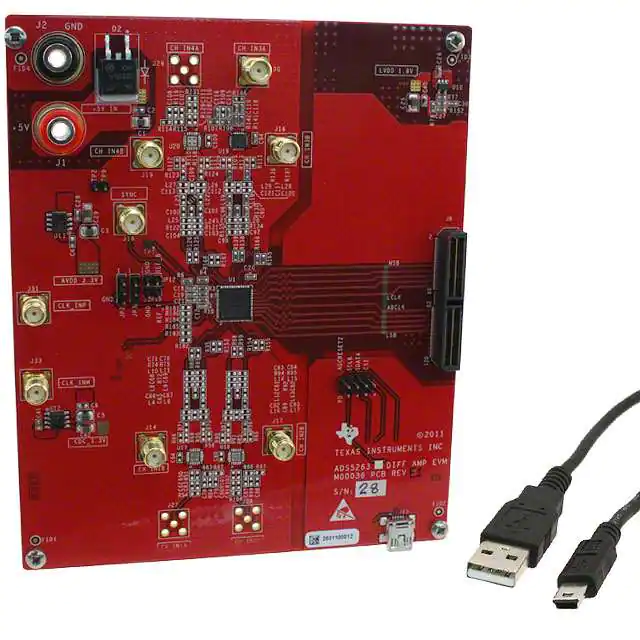
ADS5263EVM Evaluation Module
This user’s guide gives an overview of the ADS5263EVM and describes how the evaluation module can
be used to evaluate the performance, functions, and features of the ADS5263 device.
Contents
Quick Look at the Evaluation Setup ....................................................................................... 2
EVM Circuit Description ..................................................................................................... 3
2.1
Power ................................................................................................................. 3
2.2
Clock Input ........................................................................................................... 3
2.3
Analog Input ......................................................................................................... 4
2.4
Onboard Band-Pass Filter in THS Path ......................................................................... 5
3
ADS5263EVM GUI .......................................................................................................... 6
3.1
Installing the EVM GUI ............................................................................................. 6
3.2
GUI Features ........................................................................................................ 8
4
TSW1400 GUI .............................................................................................................. 10
4.1
Verify the Setup ................................................................................................... 10
4.2
Verify the Ramp Test Pattern .................................................................................... 13
4.3
Verify With a Sine Wave Analog Input ......................................................................... 15
5
ADS5263EVM Schematics and Test Points ............................................................................ 16
5.1
List of Test Points ................................................................................................. 16
6
ADS5263EVM PCB Layout ............................................................................................... 16
7
Bill of Materials ............................................................................................................. 23
Appendix A
High Speed Data Converter Pro (HSDCPro) GUI Installation ............................................... 25
1
2
List of Figures
1
Evaluation Setup ............................................................................................................. 2
2
ADS5263 Sine Wave Clocking Using Transformer
3
ADS5263 Clocking Using a LVPECL Buffer
4
5
6
7
8
9
10
11
12
13
14
15
16
17
18
19
20
..................................................................... 3
............................................................................. 4
Input Drive Circuit – Using Transformers ................................................................................. 4
Input Drive Circuit – Using THS770006 Amplifier ....................................................................... 5
Band-Pass Filter ............................................................................................................. 6
ADS5263 GUI ................................................................................................................ 9
ADS5263 GUI ............................................................................................................... 10
EVM and TSW Card Connections ....................................................................................... 11
Initializing the ADS5263GUI .............................................................................................. 12
Successful Interface Between TSW Card and Computer ............................................................. 13
Enabling Ramp Test Pattern in the ADS5263 GUI .................................................................... 14
Verifying With Ramp Test Pattern ....................................................................................... 15
Spectrum of Captured Data ............................................................................................... 16
ADS5263EVM Top Layer Assembly Drawing – Top View ............................................................ 17
ADS5263EVM Bottom Layer Assembly Drawing – Bottom View .................................................... 18
ADS5263EVM Top Layer Copper – Top View ......................................................................... 19
ADS5263EVM Internal Layer 1, Ground – Top View .................................................................. 20
ADS5263EVM Internal Layer 2, Power – Top View ................................................................... 21
ADS5263EVM Bottom Layer Copper – Top View ..................................................................... 22
SLAU344A – May 2011 – Revised March 2015
Submit Documentation Feedback
ADS5263EVM Evaluation Module
Copyright © 2011–2015, Texas Instruments Incorporated
1
�Quick Look at the Evaluation Setup
www.ti.com
21
HSDCPro Install (Begin)................................................................................................... 25
22
HSDCPro Install (Install Directory) ....................................................................................... 26
23
HSDCPro Install (TI License Agreement) ............................................................................... 27
24
HSDCPro Install (NI License Agreement) ............................................................................... 28
25
HSDCPro Install (Start Installation) ...................................................................................... 29
26
HSDCPro Install (Installation Progress) ................................................................................. 30
27
HSDCPro Install (Installation Complete) ................................................................................ 31
28
HSDCPro Install (h) ........................................................................................................ 32
29
HSDCPro Install ............................................................................................................ 32
List of Tables
1
1
Two-Input Configurations ................................................................................................... 5
2
SMT Resistors................................................................................................................ 5
3
EVM Components List ..................................................................................................... 23
Quick Look at the Evaluation Setup
Figure 1 shows an overview of the evaluation setup that includes the ADS5263EVM evaluation module
(EVM), TSW1400 capture card, external equipment, and software requirements.
Figure 1. Evaluation Setup
2
ADS5263EVM Evaluation Module
SLAU344A – May 2011 – Revised March 2015
Submit Documentation Feedback
Copyright © 2011–2015, Texas Instruments Incorporated
�EVM Circuit Description
www.ti.com
TSW1400 Capture Card: The high-speed LVDS deserializer card is required for capturing data from the
ADS5263EVM and its analysis using the TSW1400 graphical user interface (GUI).
For information pertaining to the TSW1400 card, see http://www.ti.com/tool/tsw1400evm.
Equipment: Signal generators (with low-phase noise) must be used as source of input signal and clock in
order to get the desired performance. Additionally, band-pass filters are required in both the signal and
clock paths to attenuate the harmonics and noise from the generators.
Power Supply: A single 5-V supply powers the EVM . The supplies for the ADS5263 device are derived
from the 5-V supply. The power supply must be able to source up to 1.5 A. A 6-V supply can power the
TSW1400 card using a laptop-style adapter.
USB Interface to PC: The USB connection from the ADS5263EVM and TSW1400 card to the personal
computer (PC) must be set up; Step 3 in Section 3.1 explains the USB driver installation.
ADS5263EVM GUI: Section 3.1 explains the GUI installation procedure and its operation.
2
EVM Circuit Description
The complete schematic of the EVM can be found at the end of this user guide. Critical portions of the
EVM are explained in the following text.
2.1
Power
The EVM requires a single 5-V supply for operation that can be supplied through banana jacks. Separate
LDOs convert the 5-V input to generate the 3.3-V AVDD supply and the 1.8-V LVDD supply required for
the ADS5263 operation.
2.2
Clock Input
The clock can be supplied to the analog-to-digital converter (ADC) in one of two ways. The default factoryconfigured option supplies a single-ended sine wave clock directly to the SMA connecter J31. This clock is
converted to differential by the TC4-1W transformer from MiniCircuits and is ac coupled to the ADC. This
transformer has an impedance ratio of 4, so the voltage applied on J31 is stepped up by a factor of 2.
The clock input must be from a clean, low-jitter source (such as SMA100A or 8644B) and filtered by a
narrow band-pass filter. Taking into account the attenuation of the filter, the clock amplitude must be set
appropriately to get about 1.5-V peak-to-peak at the clock pins of the ADS5263.
The clock source is commonly synchronized with the signal generator of the input frequency to keep the
clock and input coherent for meaningful FFT analysis.
Figure 2. ADS5263 Sine Wave Clocking Using Transformer
LVPECL Clock Option
Alternately, the clock may be supplied by an onboard LVPECL clock buffer (TI’s CDCLVP1102). To use
this option,
SLAU344A – May 2011 – Revised March 2015
Submit Documentation Feedback
ADS5263EVM Evaluation Module
Copyright © 2011–2015, Texas Instruments Incorporated
3
�EVM Circuit Description
•
•
•
www.ti.com
Remove the coupling capacitors C59, C61.
Replace the 0-Ω resistors with 0.1-µF capacitors.
Apply a single-ended, square-wave clock signal on SMA connector J33.
Figure 3. ADS5263 Clocking Using a LVPECL Buffer
2.3
Analog Input
The ADS5263 can be used as a quad-channel, 16-bit ADC or as a quad-channel, 14-bit ADC. Each
channel can be configured to use either a transformer-coupled input or a TH77006 amplifier input, from a
single-ended source. As a result, two input configurations exist detailed in Table 1.
Figure 4. Input Drive Circuit – Using Transformers
4
ADS5263EVM Evaluation Module
SLAU344A – May 2011 – Revised March 2015
Submit Documentation Feedback
Copyright © 2011–2015, Texas Instruments Incorporated
�EVM Circuit Description
www.ti.com
Figure 5. Input Drive Circuit – Using THS770006 Amplifier
Table 1. Two-Input Configurations
EVM
Config
Transformer Drive
THS770006 Drive
1
On channels 1, 2, 3, 4
On channel 3
Description
● All components in the transformer drive path for all four
channels are available in the EVM.
● All components in the THS path for only channel 3 is available
in the EVM.
2
On channels 1, 2, 3, 4
On channels 1, 2, 3,
4
● All components in the transformer and THS paths for all four
channels are available in the EVM.
Note that the 16-bit ADC and the 14-bit ADC have different analog input pins. Analog input pins 1A, 2A,
3A, 4A correspond to the 16-bit ADC inputs while 1B, 2B, 3B, 4B correspond to the 14-bit ADC inputs.
Each of the four transformer paths can be configured to drive either the 16-bit or 14-bit ADC inputs.
Similarly, each of the four THS paths can be configured to drive either the 16-bit or 14-bit ADC inputs.
This configuration is achieved using pairs of 0 Ω SMT resistors, as listed in Table 2.
Table 2. SMT Resistors
2.4
Drive Type
Chan 1A
16-Bit ADC
Chan 1B
14-Bit ADC
Chan 2A
16-Bit ADC
Chan 2B
14-Bit ADC
Transformer
R80,R81 = Open
R169,R170 = 0 Ω
R35, R153 =Open
R169, R170 = Open
R35, R153 = 0 Ω
R98, R99 = Open
R171, R172 = 0 Ω
R154, R155 = Open
R171, R172 = Open
R154, R155 = 0 Ω
THS770006
R80, R81 = 0 Ω
R169, R170 = Open
This option is not supported
R98, R99 = 0 Ω
R171, R172 = Open
This option is not supported
Drive Type
Chan 3A
16-Bit ADC
Chan 3B
14-Bit ADC
Chan 4A
16-Bit ADC
Chan 4B
14-Bit ADC
Transformer
R138,R139 = Open
R173, R174 = 0 Ω
R165, R166 = Open
R173, R174 = Open
R165, R166 = 0 Ω
R125, R126 = Open
R175, R176 = 0 Ω
R167, R168 = Open
R175, R176 = Open
R167, R168 = 0 Ω
THS770006
R138, R139 = 0 Ω
R173, R174 = Open
This option is not supported
R125, R126 = 0 Ω
R175, R176 = Open
This option is not supported
Onboard Band-Pass Filter in THS Path
A provision exists in the EVM to include a band-pass filter in the analog input between the THS770006
amplifier and the ADS5263 input pins. Component placeholders are provided to support up to sixth-order
LC band-pass filter on each of the four channels. This allows users to design their own filters, populate the
EVM with the corresponding components, and verify the performance on the EVM itself.
SLAU344A – May 2011 – Revised March 2015
Submit Documentation Feedback
ADS5263EVM Evaluation Module
Copyright © 2011–2015, Texas Instruments Incorporated
5
�ADS5263EVM GUI
www.ti.com
Figure 6. Band-Pass Filter
3
ADS5263EVM GUI
This section describes the software features accompanying the EVM kit. The ADS5263EVM control
software allows users to write to the ADC registers found in the data sheet.
3.1
Installing the EVM GUI
The ADS5263EVM comes with a software install. To Download the software, visit the ADS5263 product
folder under Tools & software.
Step 1 – Install the software before plugging in the USB cable for the first time.
• Unzip the installer file, and run the setup.exe file
Step 2 – Connect the USB cable from the PC to the EVM.
• If the USB driver has not been previously installed in the PC, then a Windows™ message Found New
Hardware appears. Proceed to Step 3 to complete the installation.
• If the message does not appear, then skip Step 3
Step 3 – Completing the USB Driver Installation
• In the Found New Hardware message, select No, not this time from the options, and press the Next
button
6
ADS5263EVM Evaluation Module
SLAU344A – May 2011 – Revised March 2015
Submit Documentation Feedback
Copyright © 2011–2015, Texas Instruments Incorporated
�ADS5263EVM GUI
www.ti.com
•
Select Install from a list or specific location (Advanced) as shown in the following illustration, and then
click Next.
•
Select Search for the best driver in these locations., and enter the file path C:\Program Files\Texas
Instruments\CDM 2.04.06 WHQL Certified in the combo-box, or browse to it by clicking the Browse
button. Once the file path has been entered in the box, click Next to proceed.
SLAU344A – May 2011 – Revised March 2015
Submit Documentation Feedback
ADS5263EVM Evaluation Module
Copyright © 2011–2015, Texas Instruments Incorporated
7
�ADS5263EVM GUI
3.2
www.ti.com
•
Windows XP can be configured to warn when unsigned (non-WHQL certified) drivers are about to be
installed. In that case, the following screen is displayed. Click on Continue Anyway to continue with the
installation.
•
If Windows XP is configured to ignore file signature warnings, no message appears.
GUI Features
Once it is launched, the ADS5263 GUI comes up in the state shown in the following illustration. The
ADS5263 has many programmable registers to control various modes. In the GUI, registers with similar
functions are grouped into separate tabs such as:
• Top-level
• Interface
• Dig Sig Proc
8
ADS5263EVM Evaluation Module
SLAU344A – May 2011 – Revised March 2015
Submit Documentation Feedback
Copyright © 2011–2015, Texas Instruments Incorporated
�ADS5263EVM GUI
www.ti.com
Figure 7. ADS5263 GUI
Additionally, the GUI has a couple of interesting features – debug mode and command sequence. The
debug mode is an alternate way of controlling the registers in the device by directly specifying the
hexadecimal values for the register address and register data.
The command sequence can be used to record and store a sequence of register writes into a text file. The
next time, after a device reset, the text file can be simply played back. The GUI configures the device with
the registers stored in the text file.
SLAU344A – May 2011 – Revised March 2015
Submit Documentation Feedback
ADS5263EVM Evaluation Module
Copyright © 2011–2015, Texas Instruments Incorporated
9
�TSW1400 GUI
www.ti.com
Figure 8. ADS5263 GUI
4
TSW1400 GUI
The TSW1400 GUI is required to transfer ADC data from the TSW1400 card. The data can be viewed in
the time-domain. The spectrum of the captured data can be viewed in the Single Tone FFT tab.
For installation of the TSW GUI, see TSW1400EVM: High-Speed LVDS Deserializer and Analysis System
user's guide. Also see Appendix Afor how to download the software.
If the PC is already pre-installed with TSW1400, it may be an earlier revision that does not support the
ADS5263 device. Follow the steps outlined in the relevant section of the TSW1400EVM user's guide to
first uninstall and then re-install the latest TSW1400 version.
4.1
Verify the Setup
Perform the following steps before launching the TSW1400 GUI:
• Connect the TSW1400 card to the ADS5263EVM.
• Connect the power supplies to both cards and power up.
• Connect the USB cables from the PC to the ADS EVM and TSW card.
10
ADS5263EVM Evaluation Module
SLAU344A – May 2011 – Revised March 2015
Submit Documentation Feedback
Copyright © 2011–2015, Texas Instruments Incorporated
�TSW1400 GUI
www.ti.com
Figure 9. EVM and TSW Card Connections
•
Launch the ADS5263GUI, and initialize the device
– First, reset the device by clicking the Self-reset button (this is a self-clearing bit that resets the
device and clears itself to zero)
– Put device in 2-wire, …modes
SLAU344A – May 2011 – Revised March 2015
Submit Documentation Feedback
ADS5263EVM Evaluation Module
Copyright © 2011–2015, Texas Instruments Incorporated
11
�TSW1400 GUI
www.ti.com
Figure 10. Initializing the ADS5263GUI
•
•
•
•
12
Apply input clock signal to SMA connector J31.
The device is now ready for data capture by the TSW card.
– Check the DCM LED on the TSW card – it must be flashing. This indicates that the TSW card is
able to correctly detect the bit clock output from the ADS EVM.
Launch the TSW GUI; at this point, the TSW GUI communicates with the EVM and once proper
communication is established, a message is displayed at the bottom left of the GUI.
This completes the setup verification.
ADS5263EVM Evaluation Module
SLAU344A – May 2011 – Revised March 2015
Submit Documentation Feedback
Copyright © 2011–2015, Texas Instruments Incorporated
�TSW1400 GUI
www.ti.com
Figure 11. Successful Interface Between TSW Card and Computer
4.2
Verify the Ramp Test Pattern
•
•
Initialize the TSW GUI with the following settings.
– Select the device.
– Choose the channel.
– Enter the ADC sample rate. For example, 80M for 80-MSPS sample rate.
Using the ADS5263 GUI, enable the Ramp Test Pattern mode
SLAU344A – May 2011 – Revised March 2015
Submit Documentation Feedback
ADS5263EVM Evaluation Module
Copyright © 2011–2015, Texas Instruments Incorporated
13
�TSW1400 GUI
www.ti.com
Figure 12. Enabling Ramp Test Pattern in the ADS5263 GUI
•
•
14
Press the Capture button in the TSW GUI.
Time Domain:
– Select the Time Domain tab in the GUI.
– Graph shows the captured time domain data.
It Must be a clean digital ramp that increases from code 0 to code 65535 from one sample to the
next. Note that the starting code in the capture graph is not fixed and can be anywhere from 0 to
65535.
ADS5263EVM Evaluation Module
SLAU344A – May 2011 – Revised March 2015
Submit Documentation Feedback
Copyright © 2011–2015, Texas Instruments Incorporated
�TSW1400 GUI
www.ti.com
Figure 13. Verifying With Ramp Test Pattern
•
•
4.3
Now, disable the Ramp Test Pattern in the ADS5263 GUI.
This completes the verification of the ramp test pattern.
Verify With a Sine Wave Analog Input
•
•
•
•
•
Note that for all performance evaluation, low-phase noise signal generators are required (see Figure 1)
for both analog signal and sampling clock inputs.
In the TSW GUI,
– Enter the ADC input frequency being applied. For example, 3M for 3-MHz input frequency.
– choose the desired channel
Set the frequency in the signal generator to the value displayed in the field ADC Input Coherent
frequency and connect the generator output to the desired channel.
This makes the input signal coherent with respect to the sampling clock, which is required for FFT
analysis.
Now, press the Capture button
Frequency Domain:
– Select the Single tone FFT tab in the GUI.
– The fft graph shows the spectrum of the captured sine wave data
SLAU344A – May 2011 – Revised March 2015
Submit Documentation Feedback
ADS5263EVM Evaluation Module
Copyright © 2011–2015, Texas Instruments Incorporated
15
�ADS5263EVM Schematics and Test Points
www.ti.com
Figure 14. Spectrum of Captured Data
5
ADS5263EVM Schematics and Test Points
The schematics for the ADS5263EVM evaluation module are attached at the end of this document.
5.1
List of Test Points
Test Points on the EVM
6
Test Points
Name
Description
TP1
SDOUT
Serial register output
TP2
Ground
Board ground
TP9
VCM
1.5V common-mode output
TP12
SDATA
Serial interface data input
TP13
SCLK
Serial interface clock input
TP14
CSZ
Serial interface enable input
TP15
ADCRESETZ
Reset input
TP16
PD
Power down control input
ADS5263EVM PCB Layout
The following figures (Figure 15 through Figure 20) show the design of the ADS5263EVM printed-circuit
board. PCB dimensions: L x W = 5 x 6 inches, four layers and 0.5-oz copper on outer layers and 1oz
copper on inner layers.
16
ADS5263EVM Evaluation Module
SLAU344A – May 2011 – Revised March 2015
Submit Documentation Feedback
Copyright © 2011–2015, Texas Instruments Incorporated
�ADS5263EVM PCB Layout
www.ti.com
Figure 15. ADS5263EVM Top Layer Assembly Drawing – Top View
SLAU344A – May 2011 – Revised March 2015
Submit Documentation Feedback
ADS5263EVM Evaluation Module
Copyright © 2011–2015, Texas Instruments Incorporated
17
�ADS5263EVM PCB Layout
www.ti.com
Figure 16. ADS5263EVM Bottom Layer Assembly Drawing – Bottom View
18
ADS5263EVM Evaluation Module
SLAU344A – May 2011 – Revised March 2015
Submit Documentation Feedback
Copyright © 2011–2015, Texas Instruments Incorporated
�ADS5263EVM PCB Layout
www.ti.com
Figure 17. ADS5263EVM Top Layer Copper – Top View
SLAU344A – May 2011 – Revised March 2015
Submit Documentation Feedback
ADS5263EVM Evaluation Module
Copyright © 2011–2015, Texas Instruments Incorporated
19
�ADS5263EVM PCB Layout
www.ti.com
Figure 18. ADS5263EVM Internal Layer 1, Ground – Top View
20
ADS5263EVM Evaluation Module
SLAU344A – May 2011 – Revised March 2015
Submit Documentation Feedback
Copyright © 2011–2015, Texas Instruments Incorporated
�ADS5263EVM PCB Layout
www.ti.com
Figure 19. ADS5263EVM Internal Layer 2, Power – Top View
SLAU344A – May 2011 – Revised March 2015
Submit Documentation Feedback
ADS5263EVM Evaluation Module
Copyright © 2011–2015, Texas Instruments Incorporated
21
�ADS5263EVM PCB Layout
www.ti.com
Figure 20. ADS5263EVM Bottom Layer Copper – Top View
22
ADS5263EVM Evaluation Module
SLAU344A – May 2011 – Revised March 2015
Submit Documentation Feedback
Copyright © 2011–2015, Texas Instruments Incorporated
�Bill of Materials
www.ti.com
7
Bill of Materials
Table 3. EVM Components List
Qty
Reference Designator
Value
Manufacturer
Part Number
Description
6
C1,C3,C5,C25,C29,C42
10 µF
AVX
1206YC106MAT2A
CAP CER 10UF 16V X7R 20% 1206
4
C2,C4,C6,C40
1 µF
AVX
0603YC105KAT2A
CAP CER 1.0UF 16V X7R 10% 0603
0.1 µF
AVX
ECJ-1VB1C104K
CAP CER .10UF 50V X7R 10% 0603
C10,C11,C12,C18,C19,C20,
C21,C26,C27,C30,C43,C44,
C45,C46,C59,C60,C61,C94,
32
C99,C115,C116,C118,C119,
C124,C125,C126,C152,C154
C28,C41,C95,C96
8
C51,C52,C53,C54,C55,C56, C57,C58
220 pF
AVX
06035A221FAT2A
CAP CERM 220PF 1% 50V NP0 0603
1
C149
10 nF
Panasonic
ECJ-1VB1C103K
CAP 10000PF 16V CERM X7R 0603
2
C150,C153
47 pF
Panasonic
ECJ-1VC1H470J
CAP CERAMIC 47PF 50V 0603 SMD
1
C151
4.7 µF
AVX
TAJA475K020R
1
D2
MBRB2515L
MBRB2515LT4GOSCT-ND
MBRB2515LT4GOSCT-ND
DIODE SCHOTTKY 15V 25A D2PAK
2
JP2,JP3
HEADER 3POS 0.1 CTR
ANY
JUMPER,3P,.100CC
JUMPER,3P,.1CC
2
JP12,JP13
HEADER_1x2_100_430L
ANY
1
J1
RED
ALLIED ELECTRONICS
ST-351A
Banana Female Red
1
J2
BLK
ALLIED ELECTRONICS
ST-351B
Banana Female Black
1
J8
QTH-060-02-F-D-A
SAMTEC
QTH-060-02-F-D-A
High speed connector
1
J13
USB_MINI_AB
JAE
DX3R005HN2E700
USB_MINI_AB
8
J14,J16,J17,J18,J19,J30,J31,J33
SMA
SAMTEC
SMA-J-P-H-ST-TH1
JACK PANEL MOUNT SMA
1
L7
1K at 100 MHz
2
L18,L19
0Ω
Panasonic
ERJ-3GEY0R00
RESISTOR,SMT,0603,0 OHM,5%,
ZERO OHM JUMPER
8
L30,L31,L32,L33,L34,L35,L36,L37
56 nH
Panasonic
EXC-ML32A680U
Inductor
23
R3,R5,R7,R9,R10,R132,
0Ω
Panasonic
ERJ-3GEY0R00
RESISTOR,SMT,0603,0 OHM,5%,
ZERO OHM JUMPER
R133,R138,R139,R141,R165,
R166,R169,R170,R171,R172,
R175,R176,R188,R189,R190,
R191,R192
2
R4,R78
56.2K
Panasonic - ECG
ERJ-3EKF5622V
RES 56.2K OHM 1/10W 1% 0603 SMD
1
R6
50 Ω
Panasonic
ERJ-3EKF49R9V
RES 49.9 OHM 1/10W 1% 0603 SMD
8
R36,R37,R38,R39,R40,R41,R42,R43
25 Ω
Panasonic
ERJ-3EKF24R9V
RES 24.9 OHM 1/10W 1% 0603 SMD
2
R45,R48
100
Panasonic
ERJ-3EKF1000V
RES 100 OHM 1/10W 1% 0603 SMD
1
R46
10 Ω
Panasonic
ERJ-3EKF10R0V
RES 10.0 OHM 1/10W 1% 0603 SMD
2
R53,R56
10K
Panasonic
ERJ-3EKF1002V
RES 10.0K OHM 1/10W 1% 0603 SMD
8
R59,R60,R61,R62,R63,R64,R65,R67
12.4 Ω
Panasonic
ERJ-3EKF12R4V
RES 12.4 OHM 1/10W 1% 0603 SMD
2
R77,R152
56K
Panasonic
ERJ-3EKF5602V
RES 56.0K OHM 1/10W 1% 0603 SMD
2
R107,R108
250 Ω
Vishay
PLT0603Z2500AST5
RES 250 OHM 0.05% 5PPM 0603 SMD
2
R134,R135
200 Ω
Panasonic
ERJ-3EKF2000V
RES 200 OHM 1/10W 1% 0603 SMD
2
R136,R137
15 Ω
Vishay
CRCW06035R10FNEA
RES 15 OHM 1/10W 1% 0603 SMD
1
R142
50 Ω
Panasonic
ERJ-3EKF49R9V
RES 49.9 OHM 1/10W 1% 0603 SMD
2
R186,R187
0Ω
Vishay/Dale
CRCW04023K00FKED
RESISTOR,SMT,0603,0 OHM,5%,
ZERO OHM JUMPER
11
TP1,TP2,TP9,TP12,TP13,
T POINT R
TP14,TP15,TP16,TP17,TP18,TP19
1
T15
TC4-1W
MINI CIRCUITS
TC4-1WG2+
Transformer
8
T26,T27,T28,T29,T30,T31,T32,T33
WBC1-1
COIL CRAFT
WBC1-1TLB
Transformer
1
U1
ADS5263_QFN64
Texas Instruments
1
U6
FT245RL
FTDI
FT245RL
IC USB TO PARALLEL FIFO 28-SSOP
1
U10
TPS73201-SOT23
Texas Instruments
TPS7320IDBVT
IC LDO REG 250MA ADJ-V SOT23-5
2
U11,U12
TPS77533D
Texas Instruments
TPS77533D
IC 3.3V 500MA LDO REG 8-SOIC
1
U19
THS770006
Texas Instruments
TPS770006IRGER
IC AMP DIFF ADC DVR 16BIT 24VQFN
1
U21
CDCLVP1102
Texas Instruments
CDCLVP1102RGTT
IC CLK BUFF 1:2 LVPECL SGL 16QFN
2
Z_SH-H3,Z_SH-H4
SHUNT-HEADER
2
Z_SH-J1,Z_SH-J2
SHUNT-JUMPER-0402
16-Bit Quad channel ADC
SLAU344A – May 2011 – Revised March 2015
Submit Documentation Feedback
ADS5263EVM Evaluation Module
Copyright © 2011–2015, Texas Instruments Incorporated
23
�Bill of Materials
www.ti.com
Table 3. EVM Components List (continued)
Qty
Manufacturer
Part Number
Description
4
STANDOFF HEX M3 THR ALUM 18MM
Digi-Key
24436K-ND
STANDOFF HEX M3 THR ALUM 18MM
4
SCREW STEEL M3 THR 6MM
Digi-Key
29311K-ND
SCREW STEEL M3 THR 6MM
24
Reference Designator
Value
ADS5263EVM Evaluation Module
SLAU344A – May 2011 – Revised March 2015
Submit Documentation Feedback
Copyright © 2011–2015, Texas Instruments Incorporated
�Appendix A
SLAU344A – May 2011 – Revised March 2015
High Speed Data Converter Pro (HSDCPro) GUI
Installation
Download the HSDCPro GUI Installer using this link: HSDCPro GUI
• Unzip the saved folder and run the installer executable to obtain the pop-up shown in Figure 21.
• Click the Install button.
Figure 21. HSDCPro Install (Begin)
•
Leave the destination directories as the default location, for the TSW1400GUI installation and press
the NEXT button as shown in Figure 22.
SLAU344A – May 2011 – Revised March 2015
Submit Documentation Feedback
High Speed Data Converter Pro (HSDCPro) GUI Installation
Copyright © 2011–2015, Texas Instruments Incorporated
25
�Appendix A
www.ti.com
Figure 22. HSDCPro Install (Install Directory)
•
26
Read the License Agreement from Texas Instruments and select I accept the License Agreement and
press the Next button as shown in Figure 23.
High Speed Data Converter Pro (HSDCPro) GUI Installation
Copyright © 2011–2015, Texas Instruments Incorporated
SLAU344A – May 2011 – Revised March 2015
Submit Documentation Feedback
�Appendix A
www.ti.com
Figure 23. HSDCPro Install (TI License Agreement)
•
Read the License Agreement from National Instruments and select I accept the License Agreement
and press the Next button as shown in Figure 24.
SLAU344A – May 2011 – Revised March 2015
Submit Documentation Feedback
High Speed Data Converter Pro (HSDCPro) GUI Installation
Copyright © 2011–2015, Texas Instruments Incorporated
27
�Appendix A
www.ti.com
Figure 24. HSDCPro Install (NI License Agreement)
•
28
Press the Next button as shown in Figure 25.
High Speed Data Converter Pro (HSDCPro) GUI Installation
Copyright © 2011–2015, Texas Instruments Incorporated
SLAU344A – May 2011 – Revised March 2015
Submit Documentation Feedback
�Appendix A
www.ti.com
Figure 25. HSDCPro Install (Start Installation)
•
The window shown in Figure 26 should appear indicating that the installation is in progress.
SLAU344A – May 2011 – Revised March 2015
Submit Documentation Feedback
High Speed Data Converter Pro (HSDCPro) GUI Installation
Copyright © 2011–2015, Texas Instruments Incorporated
29
�Appendix A
www.ti.com
Figure 26. HSDCPro Install (Installation Progress)
•
30
The window shown in Figure 27 appears indicating Installation Complete. Press the Next button.
High Speed Data Converter Pro (HSDCPro) GUI Installation
Copyright © 2011–2015, Texas Instruments Incorporated
SLAU344A – May 2011 – Revised March 2015
Submit Documentation Feedback
�Appendix A
www.ti.com
Figure 27. HSDCPro Install (Installation Complete)
•
The window shown in Figure 28 appears briefly to complete the process.
SLAU344A – May 2011 – Revised March 2015
Submit Documentation Feedback
High Speed Data Converter Pro (HSDCPro) GUI Installation
Copyright © 2011–2015, Texas Instruments Incorporated
31
�Appendix A
www.ti.com
Figure 28. HSDCPro Install (h)
•
As shown in Figure 29 a restart might be requested depending on whether or not the PC already had
the National Instruments MCR Installer. If requested, hit the Restart button to complete the installation.
Figure 29. HSDCPro Install
32
High Speed Data Converter Pro (HSDCPro) GUI Installation
Copyright © 2011–2015, Texas Instruments Incorporated
SLAU344A – May 2011 – Revised March 2015
Submit Documentation Feedback
�5
4
3
2
1
D
D
EVM CONFIGURATION MODES
DEFAULT ( SINGLE AMP ) CONFIGURATION
Default Config (with transformer drive on 3 channels &
C
C
THS770006 on one channel ( IN3A)
OPTIONAL ( 4 CHANNEL AMP ) CONFIGURATION
THS7700 Config - THS770006-based drive on all 4 channels
B
B
Channel ( IN1A, IN2A, IN3A IN4A)
A
A
Title
ADS5263EVM
Size
A
Date:
5
4
3
EDGE No : 6526733
ECR No : 2115370
Tuesday, May 03, 2011
2
Rev
EVM CONFIGURATION
Sheet
1
of
1
A
8
�5
4
3
2
1
5V
J1
+5V_IN
E
E
1
1
RED
D2
6.3V
+ 10UF
C1
6.3V
1uF
C2
J2
GND
3
1
2
MBRB2515L
2
4
5V_IN
GND
BLK
GND
D
D
+3.3V_AVDD
5V
+1.8V_LVDD
5V
U10
R77
56K
R152
56K
EN
C27
.1uF
16V
C30
.1uF
16V
+
GND RESET
EN
NC
IN
OUT1
IN1
OUT
1
2
C40
1uF
6.3V
8
7
6
5
C3
+ 10UF
6.3V
2
4
1
2
3
4
C4
1uF
6.3V
2
3
GND
NC/FB
C25
10UF
6.3V
1
2
1.8V
1
OUT
C26
.1uF
16V
5
1
U11
IN
2
1
TPS73201-SOT23
C
C28
0.1uF
16V
R78
56.2K
GND
C
TPS77533D
C29
10uF
16V
GND
GND
GND
B
B
CDC_3.3V
5V
C41
0.1uF
16V
2
C5
+ 10UF
6.3V
C6
1
GND RESET
EN
NC
IN
OUT1
IN1
OUT
8
7
6
5
1uF
6.3V
2
1
2
3
4
1
U12
TPS77533D
C42
10uF
16V
A
A
Title
ADS5263EVM
Size
B
Date:
5
4
3
2
EDGE No : 6526733
ECR No : 2115370
Tuesday, May 03, 2011
Rev
Power Supply
Sheet
1
A
2
of
8
�5
4
3
2
1
J8A
QTH-060-02-F-D-A
PLACE 0.1UF CLOSE TO DEVICE AVDD PINS
C10
.1uF
1
2
2
+3.3V_AVDD
1
+3.3V_AVDD
2
4
6
8
10
12
14
16
18
20
22
24
26
28
30
32
34
36
38
40
42
44
46
48
50
52
54
56
58
60
C12
.1uF
E
Do not Install R5
R5
REFB
1
1
0 ohm
R7
0 OHM
Do not Install R7, C19
DEFAULT: SHORT 1 & 2
1
C19
.1uF
REFB
2
1
JP12
2
TP9
3
1
+3.3V_AVDD
TP2
OUT8M
OUT8P
VCM
JP2
2
OUT7M
OUT7P
OUT5M
OUT5P
JP3
2
LCLKM
LCLKP
R56
10K
1
CLKN
CLKP
REFT
REFB
2
R4
1
2
J18
SMA
R6
1
2
56.2K
122
124
AMS
DNE
50 Ohms
+3.3V_AVDD
.1uF
2
1
C11
ADCRESETZ
1
64
63
62
61
60
59
58
57
56
55
54
53
52
51
50
49
IN1B_P
IN1B_M
IN2A_P
IN2A_M
IN2B_P
IN2B_M
R46
1
B
PD
2
2
10 ohm
OUT1P
OUT1M
RESETZ
SCLK
SDATA
CSZ
AVDD
CLKM
CLKP
AVDD
INT/EXTZ
REFT
REFB
VCM
NC
ISET
AVDD
SYNC
IN1A_P
IN1A_M
AGND
IN1B_P
IN1B_M
AGND
IN2A_P
IN2A_M
AGND
IN2B_P
IN2B_M
LGND
PD
LGND
OUT1P
OUT1M
U1
ADS5263_QFN64
IN4A_M
IN4A_P
AGND
IN4B_M
IN4B_P
AGND
IN3A_M
IN3A_P
AGND
IN3B_M
IN3B_P
AGND
LGND
LVDD
OUT8M
OUT8P
48
47
46
45
44
43
42
41
40
39
38
37
36
35
34
33
OUT3M
OUT3P
IN4A_M
IN4A_P
OUT2M
OUT2P
IN4B_M
IN4B_P
OUT1M
OUT1P
IN3A_M
IN3A_P
IN3B_M
IN3B_P
+1.8V_LVDD
2
1
.1uF C20
OUT8M
OUT8P
17
18
19
20
21
22
23
24
25
26
27
28
29
30
31
32
1
R53
10K
OUT4M
OUT4P
OUT2P
OUT2M
OUT3P
OUT3M
OUT4P
OUT4M
ADCLKP
ADCLKM
LCLKP
LCLKM
OUT5P
OUT5M
OUT6P
OUT6M
OUT7P
OUT7M
IN1A_P
IN1A_M
1
2
3
4
5
6
7
8
9
10
11
12
13
14
15
16
GND
62
64
66
68
70
72
74
76
78
80
82
84
86
88
90
92
94
96
98
100
102
104
106
108
110
112
114
116
118
120
ADCLKM
ADCLKP
C
65
126
128
ADCLKP
ADCLKM
LCLKP
LCLKM
GND
GND
GND
GND
62
64
66
68
70
72
74
76
78
80
82
84
86
88
90
92
94
96
98
100
102
104
106
108
110
112
114
116
118
120
61
63
65
67
69
71
73
75
77
79
81
83
85
87
89
91
93
95
97
99
101
103
105
107
109
111
113
115
117
119
GND
GND
GND
GND
1
3
5
7
9
11
13
15
17
19
21
23
25
27
29
31
33
35
37
39
41
43
45
47
49
51
53
55
57
59
E
D
121
123
61
63
65
67
69
71
73
75
77
79
81
83
85
87
89
91
93
95
97
99
101
103
105
107
109
111
113
115
117
119
C
B
125
127
J8B
QTH-060-02-F-D-A
OUT5P
OUT5M
OUT6P
OUT6M
OUT7P
OUT7M
OUT2P
OUT2M
OUT3P
OUT3M
OUT4P
OUT4M
A
1
3
5
7
9
11
13
15
17
19
21
23
25
27
29
31
33
35
37
39
41
43
45
47
49
51
53
55
57
59
4
3
2
5
+3.3V_AVDD
Do not Install R10,C21
+3.3V_AVDD
2
REFT
1
C21
.1uF
R3
0 OHM
TP1
SCLK
SDATA
CSZ
R10
0 OHM
REFT
2
0 ohm
1
1
3
R9
2 2
OUT6M
OUT6P
DEFAULT: SHORT 1 & 2
1
Do not Install R9
JP13
1
1
C18
1
2
.1uF
D
2
4
6
8
10
12
14
16
18
20
22
24
26
28
30
32
34
36
38
40
42
44
46
48
50
52
54
56
58
60
A
Title
ADS5263EVM
Size
B
Date:
5
4
3
2
EDGE No : 6526733
ECR No : 2115370
Tuesday, May 03, 2011
Rev
ADC
A
Sheet
1
3
of
8
�5
4
3
2
1
E
E
1
4
3
4
3
2
5
S MA
1
5
2
GND
6
1
END
D
C60
.1uF
16V
R48
100
1/10W
1%
T15
GND
GND
2
CLK-
CLKN
.1uF 16V
R45
100
1/10W
1%
TC4-1W
SMA
J31
C59
D
1
C61
2
CLK+
CLKP
.1uF 16V
CDC_3.3V
CDC_3.3V CDC_3.3V
R182
82ohm
82 ohm
*
R184
0 ohm
2
U21
*
2
GND
C126
.1uF
16V
R180
C125
.1uF
16V
1
C
1
C
1
.1uF 16V
GND
GND
B
NC1
NC2
NC3
NC4
NC5
NC6
OUTP1
OUTN1
GND
GND
EP_GND
11
12
*
1
1
16
17
*
2
CLKN
R185
0 ohm
*
GND
GND
R183
2
3
4
13
14
15
9
10
130 ohm
C124
2
OUTP0
OUTN0
1
4
3
2
5
1
INP
INN
2
6
7
130 ohm
1
END
CLKP
*
GND
1
S MA
VAC_REF
2
J33
VCC
2
8
R181
SMA
CDCLVP1102
5
B
GND
A
A
Title
ADS5263EVM
Size
B
Date:
5
4
3
2
EDGE No : 6526733
ECR No : 2115370
Tuesday, May 03, 2011
Rev
ADC Clocking
Sheet
1
A
4
of
8
�5
4
3
2
1
E
E
L7
1
2
1K @ 100MHZ
J13
USB
D
6
7
8
9
VBUS
GND1
DGND2 D+
GND3
ID
GND4 GND
C154 + C151
.1uF
4.7uF
20V
C149
10nF
1
2
3
4
5
20
16
15
C150
47pF
C153
47pF
4
8
USB_MINI_AB
19
24
27
R187
0 Ohm
1
2
28
C
17
GND
R186
0 Ohm
1
2
GND
C152
.1uF
D
TP13
0 OHM
U6
25
7
18
21
26
VCC
D0
USBDM
D1
USBDP
D2
VCCIO
D3
NC1
D4
RESET
D5
NC2
D6
OSCI
D7
OSCO
RXF
3V3OUT
AGND
GND
GND
GND
TEST
TXE
RD
WR
PWREN
1
1
2
5
TP12
0 OHM
3
1
11
2
R189
0 OHM
2
1
9
2
1
6
CSZ
TP15
2
R191
0 OHM
23
SDATA
TP14
R190
0 OHM
10
1
22
SCLK
R188
ADCRESETZ
TP16
C
2
PD
R192
13
TP17
14
TP18
12
TP19
FT245RL
B
B
A
A
Title
ADS5263EVM
Size
B
Date:
5
4
3
2
EDGE No : 6526733
ECR No : 2115370
Tuesday, May 03, 2011
Rev
USB Serial Interface
Sheet
1
5
A
of
8
�5
4
3
2
1
5V
*
C79
* .1uF
VCM
R58
*
*
2
1
C87
.1uF
2
*
1
R89
*
L11
*
C76
D
*
C69
IN1A_M
*
C92
*
IN2_M
R171
C81
2 1 *1
*
*
0.1 Uf
L14
10 nH
*
*
1
L17
R86
*
1
2
*
0 Ohm
L13
R92
R93
*
0 ohm
*
0 ohm
0.1 Uf
2 1
1
*
C82
R95 *
200 ohm
L15
10 nH
*
*
2
*
R98
*
C83
1
C85
.1uF
*
R96
15 ohm
*
*
B
C84
R99
IN2A_M
*
0 ohm
R172
VCM
IN2_P
A
Title
ADS5263EVM
VCM
Size
A
Date:
4
C
0 ohm
IN2A_P
1
1
*
R85
R94
200 ohm *
2
1
R97 *
15 ohm
2
*
2
C89
R91
1
18
17
16
15
14
13
*
R87
250 ohm
*
C88
.1uF
A
5
0 Ohm
R170
IN1_P
2
2
2
1
R90
1
1
2
*
R88
250 ohm
R75
*
200 ohm
R81
1
*
25
7
8
9
10
11
12
1
C91
.1uF
*
0 Ohm
C93
5V
*
0 ohm
2
L12
2
B
*
2 1
2
2
.1uF
NC7
SF+
Unused1 U18
NC4
VIN- THS770006VOUT+
VIN+
VOUTCM
NC3
NC8
SFPAD
NC1
GND1
GND2
GND3
GND4
NC2
R104
*
4
3
2
5
1
2
3
4
50 ohm 5
6
R102 *
C90 *
R101
1
2
0 ohm
*
END
*
0 ohm
* Denotes components uninstalled in default configuration
NC6 24
VS1 23
22
VS2
21
VS3 20
VS4 19
NC5
*
1
R73
0.1 Uf
C67 *
L9
0 Ohm
L16
S MA
2
1
*
C80 .1uF
1
2
J28
C70
.1uF
*
L6
E
C71
2
1
2
*
R72
2
R70
15 ohm
*
*
5V
C
SMA
L10
2
*
2
2
1
C65
2
R71
15 ohm
1
2
C78
.1uF
R74
200 ohm *
VCM
R84
*
1
*
R82
250 ohm
1
2
*
R83
250 ohm
R80
0.1 Uf
*
D
5V
C66 *
1
*
IN1A_P
*
1
R55
*
1
1
1
C63
* .1uF
18
17
16
15
14
13
2 1
1
.1uF
2
4
3
2
5
R54
*
NC7
SF+
Unused1 U17
NC4
VIN- THS770006 VOUT+
VIN+
VOUTCM
NC3
NC8
SF-
C68
*
2
END
1
2
3
4
50 ohm 5
*
6
R51
R50
0 ohm
*
*
R69
L4
1
C62 *
1
2
1
*
R66
1
S MA
PAD
NC1
GND1
GND2
GND3
GND4
NC2
J27
25
7
8
9
10
11
12
*
SMA
*
NC6
VS1
VS2
VS3
VS4
NC5
*
2
*
L8
0 Ohm
2
24
23
22
21
20
19
E
2
C64 .1uF
1
2
*
IN1_M
R169
0 ohm
Rev
EDGE No : 6526733
ECR No : 2115370
16 Bit AMP Input Path
Sheet
Tuesday, May 03, 2011
3
6
of
A
8
2
1
�5
4
3
2
1
IN3_M
5V
0 Ohms
2 1
R106
L29
1
1
2
1
1
2
2 1
2
C116
.1uF
1
2
2
R175
0 ohm
L24
R121
200 ohm *
*
*
R112
*
1
1
R119
*
R120
*
0 ohm
0 ohm
2
C105
.1uF
R122
200 ohm *
L25
*
*
1
2
*
R114
250 ohm
*
C108
.1uF
B
*
C104
0.1 Uf
2 1
1
*
C102
L23 *
0 Ohm
R126
*
IN4A_M
0 ohm
R176
IN4_P
VCM
A
Title
ADS5263EVM
VCM
A
Date:
4
IN4A_P
*
L27
*
*
R125
C103
2
R123
15 ohm
*
*
1
R110
*
R124
15 ohm
C109
*
2
R118
1
18
17
16
15
14
13
2
0.1 Uf
*
Size
5
*
IN3_P
C101
2 1 *1
C112
*
1
2
1
2
R174
1
C111
.1uF
5V
1
C96
*
C113
A
IN3A_M
2
*
R115
250 ohm
*
*
R116
C107
*
.1uF
D
0 ohm
2
2
2
2
1
2
B
R117
1
R131
NC7
SF+
Unused1 U20
NC4
VIN- THS770006VOUT+
VIN+
VOUTCM
NC3
NC8
SF-
*
0 Ohm
L22*
2
4
3
2
5
*
1
2
3
4
50 *ohm 5
6
R129
R128
0 ohm
*
PAD
NC1
GND1
GND2
GND3
GND4
NC2
1
END
1
C
25
7
8
9
10
11
12
S MA
R139
IN4_M
NC6 24
VS1 23
22
VS2
21
VS3 20
VS4 19
NC5
*
J29
C98
*
5V
L26
C110.1uF
1
2
*
R135
200 ohm
* Denotes components uninstalled in default configuration
C100.1uF
1
2
*
SMA
0 ohm
VCM
VCM
C
L19
0 Ohms
2
2
1
R109
*
1
5V
C115
.1uF
0 ohm
0.1Uf
C121
R107
250 ohm
*
R133
*
*
D
R108
250 ohm
C99
.1uF
L21
*
C97
1
*
1
2
C117
1
NC6
VS1
VS2
VS3
VS4
NC5
*
R136
15 ohm
R132
E
1
R105
R134
200 ohm
IN3A_P
0 ohm
R138
1
1
C119
.1uF
*
1
.1uF
R137
15 ohm
0.1Uf
L20
*
2
R144
R113 *
18
17
16
15
14
13
L28
*
R111
1
*
2
4
3
2
5
END
PAD
NC1
GND1
GND2
GND3
GND4
NC2
1
NC7
SF+
Unused1 U19
NC4
VIN- THS770006VOUT+
VIN+
VOUTCM
NC3
NC8
SF25
7
8
9
10
11
12
J30
S MA
1
2
3
4
50 ohm 5
6
R142
C118
R141
0 ohm
1
2
SMA
*
2
24
23
22
21
20
19
C120
*
1
2
E
R173
C95
2
L18
2
*
2
2
C94 .1uF
1
2
Rev
EDGE No : 6526733
ECR No : 2115370
16 Bit AMP Input Path
Tuesday, May 03, 2011
3
Sheet
7
of
A
8
2
1
�5
4
3
2
1
* Denotes components uninstalled in default configuration
E
E
VCM
4
2
2
5
4
1
3
6
D
1
R60
12.4 Ohm
1
5
T30
WBC1-1
2
L31
56 nH
C52
220 pF
1
SMA
J16
C43
.1uF
R59
12.4 Ohm
END
4
3
2
5
R36
25 ohm
WBC1-1
T28
1
6
3
1
4
5
2
2
5
4
1
3
6
*
1
R165
0 ohm
R40
25 ohm
C44
.1uF
1
R63
12.4 Ohm
T33
WBC1-1
R153
0 ohm
IN3_P
IN3B_P
C57
220 pF
R64
12.4 Ohm
END
2
R38
25 ohm
S MA
2
1
L34
56 nH
1
3
2
L35
56 nH
2
IN1B_M
1
C53
220 pF
2
R41
25 ohm
D
R166
0 ohm
IN3B_M
2
6
R35
0 ohm
4
3
2
5
WBC1-1
T26
1
1
IN1B_P
C51
220 pF
2
S MA
L30
56 nH
2
SMA
J14
VCM
IN1_P
*
2
1
1
IN1_M
IN3_M
VCM
6
3
1
4
2
2
5
4
1
3
6
WBC1-1
1
R61
12.4 Ohm
1
4
3
2
5
5
T31
2
L33
56 nH
1
C55
220 pF
R39
25 ohm
S MA
WBC1-1
T29
1
6
3
1
2
J19
C45
.1uF
R62
12.4 Ohm
END
SMA
R154
0 ohm
R37
25 ohm
L36
56 nH
4
IN4B_P
C58
220 pF
R167
0 ohm
R42
25 ohm
END
5
2
2
5
4
1
3
6
C
C46
.1uF
R67
12.4 Ohm
1
2
2
R65
12.4 Ohm
1
1
C56
220 pF
IN4_P
*
T32
WBC1-1
R155
0 ohm
L37
56 nH
2
1
C54
220 pF
R43
25 ohm
R168
0 ohm
IN4B_M
2
S MA
2
IN2B_P
4
3
2
5
J17
L32
56 nH
WBC1-1
T27
2
SMA
1
*
*
IN2B_M
2
C
2
1
1
IN2_P
1
VCM
*
IN4_M
IN2_M
B
B
A
A
Title
ADS5263EVM
Size
B
Date:
5
4
3
2
EDGE No : 6526733
ECR No : 2115370
Tuesday, May 03, 2011
Rev
Transformer Drive Circuit
Sheet
1
8
of
A
8
�Revision History
www.ti.com
Revision History
Changes from Original (May 2011) to A Revision ........................................................................................................... Page
•
Changed Appendix A to TSW1400 software. ........................................................................................ 25
NOTE: Page numbers for previous revisions may differ from page numbers in the current version.
SLAU344A – May 2011 – Revised March 2015
Submit Documentation Feedback
Revision History
Copyright © 2011–2015, Texas Instruments Incorporated
33
�STANDARD TERMS AND CONDITIONS FOR EVALUATION MODULES
1.
Delivery: TI delivers TI evaluation boards, kits, or modules, including any accompanying demonstration software, components, or
documentation (collectively, an “EVM” or “EVMs”) to the User (“User”) in accordance with the terms and conditions set forth herein.
Acceptance of the EVM is expressly subject to the following terms and conditions.
1.1 EVMs are intended solely for product or software developers for use in a research and development setting to facilitate feasibility
evaluation, experimentation, or scientific analysis of TI semiconductors products. EVMs have no direct function and are not
finished products. EVMs shall not be directly or indirectly assembled as a part or subassembly in any finished product. For
clarification, any software or software tools provided with the EVM (“Software”) shall not be subject to the terms and conditions
set forth herein but rather shall be subject to the applicable terms and conditions that accompany such Software
1.2 EVMs are not intended for consumer or household use. EVMs may not be sold, sublicensed, leased, rented, loaned, assigned,
or otherwise distributed for commercial purposes by Users, in whole or in part, or used in any finished product or production
system.
2
Limited Warranty and Related Remedies/Disclaimers:
2.1 These terms and conditions do not apply to Software. The warranty, if any, for Software is covered in the applicable Software
License Agreement.
2.2 TI warrants that the TI EVM will conform to TI's published specifications for ninety (90) days after the date TI delivers such EVM
to User. Notwithstanding the foregoing, TI shall not be liable for any defects that are caused by neglect, misuse or mistreatment
by an entity other than TI, including improper installation or testing, or for any EVMs that have been altered or modified in any
way by an entity other than TI. Moreover, TI shall not be liable for any defects that result from User's design, specifications or
instructions for such EVMs. Testing and other quality control techniques are used to the extent TI deems necessary or as
mandated by government requirements. TI does not test all parameters of each EVM.
2.3 If any EVM fails to conform to the warranty set forth above, TI's sole liability shall be at its option to repair or replace such EVM,
or credit User's account for such EVM. TI's liability under this warranty shall be limited to EVMs that are returned during the
warranty period to the address designated by TI and that are determined by TI not to conform to such warranty. If TI elects to
repair or replace such EVM, TI shall have a reasonable time to repair such EVM or provide replacements. Repaired EVMs shall
be warranted for the remainder of the original warranty period. Replaced EVMs shall be warranted for a new full ninety (90) day
warranty period.
3
Regulatory Notices:
3.1 United States
3.1.1
Notice applicable to EVMs not FCC-Approved:
This kit is designed to allow product developers to evaluate electronic components, circuitry, or software associated with the kit
to determine whether to incorporate such items in a finished product and software developers to write software applications for
use with the end product. This kit is not a finished product and when assembled may not be resold or otherwise marketed unless
all required FCC equipment authorizations are first obtained. Operation is subject to the condition that this product not cause
harmful interference to licensed radio stations and that this product accept harmful interference. Unless the assembled kit is
designed to operate under part 15, part 18 or part 95 of this chapter, the operator of the kit must operate under the authority of
an FCC license holder or must secure an experimental authorization under part 5 of this chapter.
3.1.2
For EVMs annotated as FCC – FEDERAL COMMUNICATIONS COMMISSION Part 15 Compliant:
CAUTION
This device complies with part 15 of the FCC Rules. Operation is subject to the following two conditions: (1) This device may not
cause harmful interference, and (2) this device must accept any interference received, including interference that may cause
undesired operation.
Changes or modifications not expressly approved by the party responsible for compliance could void the user's authority to
operate the equipment.
FCC Interference Statement for Class A EVM devices
NOTE: This equipment has been tested and found to comply with the limits for a Class A digital device, pursuant to part 15 of
the FCC Rules. These limits are designed to provide reasonable protection against harmful interference when the equipment is
operated in a commercial environment. This equipment generates, uses, and can radiate radio frequency energy and, if not
installed and used in accordance with the instruction manual, may cause harmful interference to radio communications.
Operation of this equipment in a residential area is likely to cause harmful interference in which case the user will be required to
correct the interference at his own expense.
SPACER
SPACER
SPACER
SPACER
SPACER
SPACER
SPACER
SPACER
�FCC Interference Statement for Class B EVM devices
NOTE: This equipment has been tested and found to comply with the limits for a Class B digital device, pursuant to part 15 of
the FCC Rules. These limits are designed to provide reasonable protection against harmful interference in a residential
installation. This equipment generates, uses and can radiate radio frequency energy and, if not installed and used in accordance
with the instructions, may cause harmful interference to radio communications. However, there is no guarantee that interference
will not occur in a particular installation. If this equipment does cause harmful interference to radio or television reception, which
can be determined by turning the equipment off and on, the user is encouraged to try to correct the interference by one or more
of the following measures:
•
•
•
•
Reorient or relocate the receiving antenna.
Increase the separation between the equipment and receiver.
Connect the equipment into an outlet on a circuit different from that to which the receiver is connected.
Consult the dealer or an experienced radio/TV technician for help.
3.2 Canada
3.2.1
For EVMs issued with an Industry Canada Certificate of Conformance to RSS-210
Concerning EVMs Including Radio Transmitters:
This device complies with Industry Canada license-exempt RSS standard(s). Operation is subject to the following two conditions:
(1) this device may not cause interference, and (2) this device must accept any interference, including interference that may
cause undesired operation of the device.
Concernant les EVMs avec appareils radio:
Le présent appareil est conforme aux CNR d'Industrie Canada applicables aux appareils radio exempts de licence. L'exploitation
est autorisée aux deux conditions suivantes: (1) l'appareil ne doit pas produire de brouillage, et (2) l'utilisateur de l'appareil doit
accepter tout brouillage radioélectrique subi, même si le brouillage est susceptible d'en compromettre le fonctionnement.
Concerning EVMs Including Detachable Antennas:
Under Industry Canada regulations, this radio transmitter may only operate using an antenna of a type and maximum (or lesser)
gain approved for the transmitter by Industry Canada. To reduce potential radio interference to other users, the antenna type
and its gain should be so chosen that the equivalent isotropically radiated power (e.i.r.p.) is not more than that necessary for
successful communication. This radio transmitter has been approved by Industry Canada to operate with the antenna types
listed in the user guide with the maximum permissible gain and required antenna impedance for each antenna type indicated.
Antenna types not included in this list, having a gain greater than the maximum gain indicated for that type, are strictly prohibited
for use with this device.
Concernant les EVMs avec antennes détachables
Conformément à la réglementation d'Industrie Canada, le présent émetteur radio peut fonctionner avec une antenne d'un type et
d'un gain maximal (ou inférieur) approuvé pour l'émetteur par Industrie Canada. Dans le but de réduire les risques de brouillage
radioélectrique à l'intention des autres utilisateurs, il faut choisir le type d'antenne et son gain de sorte que la puissance isotrope
rayonnée équivalente (p.i.r.e.) ne dépasse pas l'intensité nécessaire à l'établissement d'une communication satisfaisante. Le
présent émetteur radio a été approuvé par Industrie Canada pour fonctionner avec les types d'antenne énumérés dans le
manuel d’usage et ayant un gain admissible maximal et l'impédance requise pour chaque type d'antenne. Les types d'antenne
non inclus dans cette liste, ou dont le gain est supérieur au gain maximal indiqué, sont strictement interdits pour l'exploitation de
l'émetteur
3.3 Japan
3.3.1
Notice for EVMs delivered in Japan: Please see http://www.tij.co.jp/lsds/ti_ja/general/eStore/notice_01.page 日本国内に
輸入される評価用キット、ボードについては、次のところをご覧ください。
http://www.tij.co.jp/lsds/ti_ja/general/eStore/notice_01.page
3.3.2
Notice for Users of EVMs Considered “Radio Frequency Products” in Japan: EVMs entering Japan are NOT certified by
TI as conforming to Technical Regulations of Radio Law of Japan.
If User uses EVMs in Japan, User is required by Radio Law of Japan to follow the instructions below with respect to EVMs:
1.
2.
3.
Use EVMs in a shielded room or any other test facility as defined in the notification #173 issued by Ministry of Internal
Affairs and Communications on March 28, 2006, based on Sub-section 1.1 of Article 6 of the Ministry’s Rule for
Enforcement of Radio Law of Japan,
Use EVMs only after User obtains the license of Test Radio Station as provided in Radio Law of Japan with respect to
EVMs, or
Use of EVMs only after User obtains the Technical Regulations Conformity Certification as provided in Radio Law of Japan
with respect to EVMs. Also, do not transfer EVMs, unless User gives the same notice above to the transferee. Please note
that if User does not follow the instructions above, User will be subject to penalties of Radio Law of Japan.
SPACER
SPACER
SPACER
SPACER
SPACER
�【無線電波を送信する製品の開発キットをお使いになる際の注意事項】
本開発キットは技術基準適合証明を受けておりません。
本製品のご使用に際しては、電波法遵守のため、以下のいずれかの措置を取っていただく必要がありますのでご注意ください。
1.
2.
3.
電波法施行規則第6条第1項第1号に基づく平成18年3月28日総務省告示第173号で定められた電波暗室等の試験設備でご使用
いただく。
実験局の免許を取得後ご使用いただく。
技術基準適合証明を取得後ご使用いただく。
なお、本製品は、上記の「ご使用にあたっての注意」を譲渡先、移転先に通知しない限り、譲渡、移転できないものとします。
上記を遵守頂けない場合は、電波法の罰則が適用される可能性があることをご留意ください。
日本テキサス・インスツルメンツ株式会社
東京都新宿区西新宿6丁目24番1号
西新宿三井ビル
3.3.3
Notice for EVMs for Power Line Communication: Please see http://www.tij.co.jp/lsds/ti_ja/general/eStore/notice_02.page
電力線搬送波通信についての開発キットをお使いになる際の注意事項については、次のところをご覧くださ
い。http://www.tij.co.jp/lsds/ti_ja/general/eStore/notice_02.page
SPACER
4
EVM Use Restrictions and Warnings:
4.1 EVMS ARE NOT FOR USE IN FUNCTIONAL SAFETY AND/OR SAFETY CRITICAL EVALUATIONS, INCLUDING BUT NOT
LIMITED TO EVALUATIONS OF LIFE SUPPORT APPLICATIONS.
4.2 User must read and apply the user guide and other available documentation provided by TI regarding the EVM prior to handling
or using the EVM, including without limitation any warning or restriction notices. The notices contain important safety information
related to, for example, temperatures and voltages.
4.3 Safety-Related Warnings and Restrictions:
4.3.1
User shall operate the EVM within TI’s recommended specifications and environmental considerations stated in the user
guide, other available documentation provided by TI, and any other applicable requirements and employ reasonable and
customary safeguards. Exceeding the specified performance ratings and specifications (including but not limited to input
and output voltage, current, power, and environmental ranges) for the EVM may cause personal injury or death, or
property damage. If there are questions concerning performance ratings and specifications, User should contact a TI
field representative prior to connecting interface electronics including input power and intended loads. Any loads applied
outside of the specified output range may also result in unintended and/or inaccurate operation and/or possible
permanent damage to the EVM and/or interface electronics. Please consult the EVM user guide prior to connecting any
load to the EVM output. If there is uncertainty as to the load specification, please contact a TI field representative.
During normal operation, even with the inputs and outputs kept within the specified allowable ranges, some circuit
components may have elevated case temperatures. These components include but are not limited to linear regulators,
switching transistors, pass transistors, current sense resistors, and heat sinks, which can be identified using the
information in the associated documentation. When working with the EVM, please be aware that the EVM may become
very warm.
4.3.2
EVMs are intended solely for use by technically qualified, professional electronics experts who are familiar with the
dangers and application risks associated with handling electrical mechanical components, systems, and subsystems.
User assumes all responsibility and liability for proper and safe handling and use of the EVM by User or its employees,
affiliates, contractors or designees. User assumes all responsibility and liability to ensure that any interfaces (electronic
and/or mechanical) between the EVM and any human body are designed with suitable isolation and means to safely
limit accessible leakage currents to minimize the risk of electrical shock hazard. User assumes all responsibility and
liability for any improper or unsafe handling or use of the EVM by User or its employees, affiliates, contractors or
designees.
4.4 User assumes all responsibility and liability to determine whether the EVM is subject to any applicable international, federal,
state, or local laws and regulations related to User’s handling and use of the EVM and, if applicable, User assumes all
responsibility and liability for compliance in all respects with such laws and regulations. User assumes all responsibility and
liability for proper disposal and recycling of the EVM consistent with all applicable international, federal, state, and local
requirements.
5.
Accuracy of Information: To the extent TI provides information on the availability and function of EVMs, TI attempts to be as accurate
as possible. However, TI does not warrant the accuracy of EVM descriptions, EVM availability or other information on its websites as
accurate, complete, reliable, current, or error-free.
SPACER
SPACER
SPACER
SPACER
SPACER
SPACER
�SPACER
6.
Disclaimers:
6.1 EXCEPT AS SET FORTH ABOVE, EVMS AND ANY WRITTEN DESIGN MATERIALS PROVIDED WITH THE EVM (AND THE
DESIGN OF THE EVM ITSELF) ARE PROVIDED "AS IS" AND "WITH ALL FAULTS." TI DISCLAIMS ALL OTHER
WARRANTIES, EXPRESS OR IMPLIED, REGARDING SUCH ITEMS, INCLUDING BUT NOT LIMITED TO ANY IMPLIED
WARRANTIES OF MERCHANTABILITY OR FITNESS FOR A PARTICULAR PURPOSE OR NON-INFRINGEMENT OF ANY
THIRD PARTY PATENTS, COPYRIGHTS, TRADE SECRETS OR OTHER INTELLECTUAL PROPERTY RIGHTS.
6.2 EXCEPT FOR THE LIMITED RIGHT TO USE THE EVM SET FORTH HEREIN, NOTHING IN THESE TERMS AND
CONDITIONS SHALL BE CONSTRUED AS GRANTING OR CONFERRING ANY RIGHTS BY LICENSE, PATENT, OR ANY
OTHER INDUSTRIAL OR INTELLECTUAL PROPERTY RIGHT OF TI, ITS SUPPLIERS/LICENSORS OR ANY OTHER THIRD
PARTY, TO USE THE EVM IN ANY FINISHED END-USER OR READY-TO-USE FINAL PRODUCT, OR FOR ANY
INVENTION, DISCOVERY OR IMPROVEMENT MADE, CONCEIVED OR ACQUIRED PRIOR TO OR AFTER DELIVERY OF
THE EVM.
7.
USER'S INDEMNITY OBLIGATIONS AND REPRESENTATIONS. USER WILL DEFEND, INDEMNIFY AND HOLD TI, ITS
LICENSORS AND THEIR REPRESENTATIVES HARMLESS FROM AND AGAINST ANY AND ALL CLAIMS, DAMAGES, LOSSES,
EXPENSES, COSTS AND LIABILITIES (COLLECTIVELY, "CLAIMS") ARISING OUT OF OR IN CONNECTION WITH ANY
HANDLING OR USE OF THE EVM THAT IS NOT IN ACCORDANCE WITH THESE TERMS AND CONDITIONS. THIS OBLIGATION
SHALL APPLY WHETHER CLAIMS ARISE UNDER STATUTE, REGULATION, OR THE LAW OF TORT, CONTRACT OR ANY
OTHER LEGAL THEORY, AND EVEN IF THE EVM FAILS TO PERFORM AS DESCRIBED OR EXPECTED.
8.
Limitations on Damages and Liability:
8.1 General Limitations. IN NO EVENT SHALL TI BE LIABLE FOR ANY SPECIAL, COLLATERAL, INDIRECT, PUNITIVE,
INCIDENTAL, CONSEQUENTIAL, OR EXEMPLARY DAMAGES IN CONNECTION WITH OR ARISING OUT OF THESE
TERMS ANDCONDITIONS OR THE USE OF THE EVMS PROVIDED HEREUNDER, REGARDLESS OF WHETHER TI HAS
BEEN ADVISED OF THE POSSIBILITY OF SUCH DAMAGES. EXCLUDED DAMAGES INCLUDE, BUT ARE NOT LIMITED
TO, COST OF REMOVAL OR REINSTALLATION, ANCILLARY COSTS TO THE PROCUREMENT OF SUBSTITUTE GOODS
OR SERVICES, RETESTING, OUTSIDE COMPUTER TIME, LABOR COSTS, LOSS OF GOODWILL, LOSS OF PROFITS,
LOSS OF SAVINGS, LOSS OF USE, LOSS OF DATA, OR BUSINESS INTERRUPTION. NO CLAIM, SUIT OR ACTION SHALL
BE BROUGHT AGAINST TI MORE THAN ONE YEAR AFTER THE RELATED CAUSE OF ACTION HAS OCCURRED.
8.2 Specific Limitations. IN NO EVENT SHALL TI'S AGGREGATE LIABILITY FROM ANY WARRANTY OR OTHER OBLIGATION
ARISING OUT OF OR IN CONNECTION WITH THESE TERMS AND CONDITIONS, OR ANY USE OF ANY TI EVM
PROVIDED HEREUNDER, EXCEED THE TOTAL AMOUNT PAID TO TI FOR THE PARTICULAR UNITS SOLD UNDER
THESE TERMS AND CONDITIONS WITH RESPECT TO WHICH LOSSES OR DAMAGES ARE CLAIMED. THE EXISTENCE
OF MORE THAN ONE CLAIM AGAINST THE PARTICULAR UNITS SOLD TO USER UNDER THESE TERMS AND
CONDITIONS SHALL NOT ENLARGE OR EXTEND THIS LIMIT.
9.
Return Policy. Except as otherwise provided, TI does not offer any refunds, returns, or exchanges. Furthermore, no return of EVM(s)
will be accepted if the package has been opened and no return of the EVM(s) will be accepted if they are damaged or otherwise not in
a resalable condition. If User feels it has been incorrectly charged for the EVM(s) it ordered or that delivery violates the applicable
order, User should contact TI. All refunds will be made in full within thirty (30) working days from the return of the components(s),
excluding any postage or packaging costs.
10. Governing Law: These terms and conditions shall be governed by and interpreted in accordance with the laws of the State of Texas,
without reference to conflict-of-laws principles. User agrees that non-exclusive jurisdiction for any dispute arising out of or relating to
these terms and conditions lies within courts located in the State of Texas and consents to venue in Dallas County, Texas.
Notwithstanding the foregoing, any judgment may be enforced in any United States or foreign court, and TI may seek injunctive relief
in any United States or foreign court.
Mailing Address: Texas Instruments, Post Office Box 655303, Dallas, Texas 75265
Copyright © 2015, Texas Instruments Incorporated
spacer
�IMPORTANT NOTICE
Texas Instruments Incorporated and its subsidiaries (TI) reserve the right to make corrections, enhancements, improvements and other
changes to its semiconductor products and services per JESD46, latest issue, and to discontinue any product or service per JESD48, latest
issue. Buyers should obtain the latest relevant information before placing orders and should verify that such information is current and
complete. All semiconductor products (also referred to herein as “components”) are sold subject to TI’s terms and conditions of sale
supplied at the time of order acknowledgment.
TI warrants performance of its components to the specifications applicable at the time of sale, in accordance with the warranty in TI’s terms
and conditions of sale of semiconductor products. Testing and other quality control techniques are used to the extent TI deems necessary
to support this warranty. Except where mandated by applicable law, testing of all parameters of each component is not necessarily
performed.
TI assumes no liability for applications assistance or the design of Buyers’ products. Buyers are responsible for their products and
applications using TI components. To minimize the risks associated with Buyers’ products and applications, Buyers should provide
adequate design and operating safeguards.
TI does not warrant or represent that any license, either express or implied, is granted under any patent right, copyright, mask work right, or
other intellectual property right relating to any combination, machine, or process in which TI components or services are used. Information
published by TI regarding third-party products or services does not constitute a license to use such products or services or a warranty or
endorsement thereof. Use of such information may require a license from a third party under the patents or other intellectual property of the
third party, or a license from TI under the patents or other intellectual property of TI.
Reproduction of significant portions of TI information in TI data books or data sheets is permissible only if reproduction is without alteration
and is accompanied by all associated warranties, conditions, limitations, and notices. TI is not responsible or liable for such altered
documentation. Information of third parties may be subject to additional restrictions.
Resale of TI components or services with statements different from or beyond the parameters stated by TI for that component or service
voids all express and any implied warranties for the associated TI component or service and is an unfair and deceptive business practice.
TI is not responsible or liable for any such statements.
Buyer acknowledges and agrees that it is solely responsible for compliance with all legal, regulatory and safety-related requirements
concerning its products, and any use of TI components in its applications, notwithstanding any applications-related information or support
that may be provided by TI. Buyer represents and agrees that it has all the necessary expertise to create and implement safeguards which
anticipate dangerous consequences of failures, monitor failures and their consequences, lessen the likelihood of failures that might cause
harm and take appropriate remedial actions. Buyer will fully indemnify TI and its representatives against any damages arising out of the use
of any TI components in safety-critical applications.
In some cases, TI components may be promoted specifically to facilitate safety-related applications. With such components, TI’s goal is to
help enable customers to design and create their own end-product solutions that meet applicable functional safety standards and
requirements. Nonetheless, such components are subject to these terms.
No TI components are authorized for use in FDA Class III (or similar life-critical medical equipment) unless authorized officers of the parties
have executed a special agreement specifically governing such use.
Only those TI components which TI has specifically designated as military grade or “enhanced plastic” are designed and intended for use in
military/aerospace applications or environments. Buyer acknowledges and agrees that any military or aerospace use of TI components
which have not been so designated is solely at the Buyer's risk, and that Buyer is solely responsible for compliance with all legal and
regulatory requirements in connection with such use.
TI has specifically designated certain components as meeting ISO/TS16949 requirements, mainly for automotive use. In any case of use of
non-designated products, TI will not be responsible for any failure to meet ISO/TS16949.
Products
Applications
Audio
www.ti.com/audio
Automotive and Transportation
www.ti.com/automotive
Amplifiers
amplifier.ti.com
Communications and Telecom
www.ti.com/communications
Data Converters
dataconverter.ti.com
Computers and Peripherals
www.ti.com/computers
DLP® Products
www.dlp.com
Consumer Electronics
www.ti.com/consumer-apps
DSP
dsp.ti.com
Energy and Lighting
www.ti.com/energy
Clocks and Timers
www.ti.com/clocks
Industrial
www.ti.com/industrial
Interface
interface.ti.com
Medical
www.ti.com/medical
Logic
logic.ti.com
Security
www.ti.com/security
Power Mgmt
power.ti.com
Space, Avionics and Defense
www.ti.com/space-avionics-defense
Microcontrollers
microcontroller.ti.com
Video and Imaging
www.ti.com/video
RFID
www.ti-rfid.com
OMAP Applications Processors
www.ti.com/omap
TI E2E Community
e2e.ti.com
Wireless Connectivity
www.ti.com/wirelessconnectivity
Mailing Address: Texas Instruments, Post Office Box 655303, Dallas, Texas 75265
Copyright © 2015, Texas Instruments Incorporated
�