ADS5292
www.ti.com
SLAS788B – NOVEMBER 2011 – REVISED JULY 2012
Octal Channel 12-Bit, 80 MSPS and Low-Power ADC
Check for Samples: ADS5292
FEATURES
DESCRIPTION
•
•
Using CMOS process technology and innovative
circuit techniques, the ADS5292 is a low power
80MSPS 8-Channel ADC. Low power consumption,
high SNR, low SFDR, and consistent overload
recovery allow users to design high performance
systems.
1
•
•
•
•
•
•
•
•
Maximum Sample Rate: 80 MSPS/12-Bit
High Signal-to-Noise Ratio
– 70-dBFS SNR at 5 MHz/80 MSPS
– 71.5-dBFS SNR at 5 MHz/80 MSPS and
Decimation Filter = 2
– 85-dBc SFDR at 5 MHz/80 MSPS
Low Power Consumption
– 48 mW/CH at 50 MSPS
– 54 mW/CH at 65 MSPS
– 66 mW/CH at 80 MSPS (2 LVDS Wire Per
Channel)
Digital Processing Block
– Programmable FIR Decimation Filter and
Oversampling to Minimize Harmonic
Interference
– Programmable IIR High Pass Filter to
Minimize DC Offset
– Programmable Digital Gain: 0 dB to 12 dB
– 2- or 4- Channel Averaging
Flexible Serialized LVDS Outputs:
– One or Two wires of LVDS Output Lines per
Channel Depending on ADC Sampling Rate
– Programmable Mapping Between ADC
Input Channels and LVDS Output PinsEases Board Design
– Variety of Test Patterns to Verify Data
Capture by FPGA/Receiver
Internal and External References
1.8V Operation for Low Power Consumption
Low-Frequency Noise Suppression
Recovery From 6-dB Overload within 1 Clock
Cycle
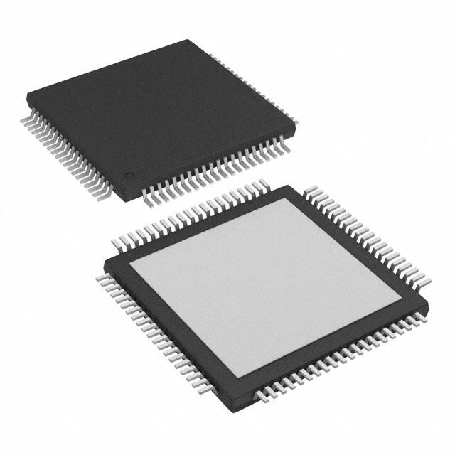
Package: 12-mm × 12-mm 80-Pin QFP
APPLICATIONS
•
•
•
Ultrasound Imaging
Communication Applications
Multi-channel Data Acquisition
The ADS5292 has a digital processing block that
integrates several commonly used digital functions for
improving system performance. It includes a digital
filter module that has built-in decimation filters (with
low-pass, high-pass and band-pass characteristics).
The decimation rate is also programmable (by 2, by
4, or by 8). This makes it useful for narrow-band
applications, where the filters can be used
conveniently to improve SNR and knock-off
harmonics, while at the same time reducing the
output data rate. The device includes an averaging
mode where two channels (or even four channels)
can be averaged to improve SNR.
Serial LVDS outputs reduce the number of interface
lines and enable the highest system integration. The
digital data from each channel ADC can be output
over one or two wires of LVDS output lines
depending on the ADC sampling rate. This 2-wire
interface helps keep the serial data rate low, allowing
low cost FPGA based receivers to be used even at
high sample rate. A unique feature is the
programmable mapping module that allows flexible
mapping between the input channels and the LVDS
output pins. This helps greatly reduce the complexity
of LVDS output routing and can potentially result in
cheaper system boards by reducing the number of
PCB layers.
The device integrates an internal reference trimmed
to accurately match across devices. Best
performance is expected to be achieved through the
internal reference mode. The device can be driven
with external references as well.
The device is available in a 12 mm × 12 mm 80-pin
QFP. It is specified over a –40°C to 85°C operating
temperature range. ADS5292 is completely pin-to-pin
and register compatible to ADS5294.
1
Please be aware that an important notice concerning availability, standard warranty, and use in critical applications of
Texas Instruments semiconductor products and disclaimers thereto appears at the end of this data sheet.
PRODUCTION DATA information is current as of publication date.
Products conform to specifications per the terms of the Texas
Instruments standard warranty. Production processing does not
necessarily include testing of all parameters.
Copyright © 2011–2012, Texas Instruments Incorporated
�ADS5292
SLAS788B – NOVEMBER 2011 – REVISED JULY 2012
www.ti.com
This integrated circuit can be damaged by ESD. Texas Instruments recommends that all integrated circuits be handled with
appropriate precautions. Failure to observe proper handling and installation procedures can cause damage.
ESD damage can range from subtle performance degradation to complete device failure. Precision integrated circuits may be more
susceptible to damage because very small parametric changes could cause the device not to meet its published specifications.
12 BIT ADC
12 BIT ADC
12 BIT ADC
12 BIT ADC
12 BIT ADC
12 BIT ADC
12 BIT ADC
12 BIT ADC
Figure 1. Block Diagram
2
Submit Documentation Feedback
Copyright © 2011–2012, Texas Instruments Incorporated
Product Folder Link(s) :ADS5292
�ADS5292
www.ti.com
SLAS788B – NOVEMBER 2011 – REVISED JULY 2012
PIN CONFIGURATION
IN2n
AGND
IN3p
IN8p
65
AGND
66
SDOUT
67
IN8n
68
AVDD
69
SYNC
70
VCM
71
NC
72
REFT
73
REFB
74
CLKp
75
AVDD
76
AVDD
77
CLKn
78
SDATA
SCLK
79
CSZ
IN1n
80
1
IN1p
IN2p
AGND
80-PIN TQFP WITH THERMAL PAD
PFP PACKAGE (TOP VIEW)
64
63
62
61
60
IN7n
2
59
IN7p
3
58
AGND
4
57
IN6n
IN3n
5
56
IN6p
AGND
6
55
AGND
IN4p
7
54
IN5n
IN4n
8
53
IN5p
52
AVDD
51
RESET
50
LGND
AVDD
Thermal Pad
9
OUT1A_n
14
47
OUT8A_p
OUT1B_p
15
46
OUT8B_n
OUT1B_n
16
45
OUT8B_p
OUT2A_p
17
44
OUT7A_n
OUT2A_n
18
43
OUT7A_p
OUT2B_p
19
42
OUT7B_n
OUT2B_n
20
21
22
23
24
25
26
27
39
41
40
OUT7B_p
OUT3A_n
OUT3B_p
OUT3B_n
OUT4A_p
OUT4A_n
OUT4B_p
OUT6A_p
OUT6A_n
30
31
32
33 34
35
36
OUT5A_n
29
OUT5B_n
28
37
38
OUT6B_p
OUT8A_n
OUT6B_n
48
OUT5A_p
13
OUT5B_p
LVDD
OUT1A_p
LCLK_p
49
LCLK_n
LGND
12
ACLK_p
11
ACLK_n
LVDD
OUT4B_n
10
OUT3A_p
ADS529X
80 TQFP
PD
PIN FUNCTIONS
PIN
NUMBER
OF PINS
NAME
5
AVDD
9, 52, 66, 71, 74
6
AGND
3, 6, 55, 58, 61, 80
2
LVDD
11, 49
Digital and I/O power supply, 1.8V
2
LGND
12, 50
Digital ground
1
CLKN
73
Negative differential clock –Tie CLKN to GND for single-ended clock
1
CLKP
72
Positive differential clock
2
LCLKP, LCLKN
31, 32
Differential LVDS bit clock (7X)
2
ACLKP, ACLKN
29, 30
Differential LVDS frame clock (1X)
2
IN1P, IN1N
78, 79
Differential input signal, Channel 1
2
IN2P, IN2N
1, 2
Differential input signal, Channel 2
2
IN3P, IN3N
4, 5
Differential input signal, Channel 3
2
IN4P, IN4N
7, 8
Differential input signal, Channel 4
2
IN5P, IN5N
53, 54
Differential input signal, Channel 5
2
IN6P, IN6N
56, 57
Differential input signal, Channel 6
2
IN7P, IN7N
59, 60
Differential input signal, Channel 7
2
IN8P, IN8N
62, 63
Differential input signal, Channel 8
2
OUT1A_P, OUT1A_N
13, 14
Differential LVDS data output, wire 1, channel 1
DESCRIPTION
NUMBER
Analog power supply, 1.8 V
Analog ground
Submit Documentation Feedback
Copyright © 2011–2012, Texas Instruments Incorporated
Product Folder Link(s) :ADS5292
3
�ADS5292
SLAS788B – NOVEMBER 2011 – REVISED JULY 2012
www.ti.com
PIN FUNCTIONS (continued)
NUMBER
OF PINS
4
PIN
NAME
DESCRIPTION
NUMBER
2
OUT1B_P, OUT1B_N
15, 16
Differential LVDS data output, wire 2, channel 1
2
OUT2A_P, OUT2A_N
17, 18
Differential LVDS data output, wire 1, channel 2
2
OUT2B_P, OUT2B_N
19, 20
Differential LVDS data output, wire 2, channel 2
2
OUT3A_P, OUT3A_N
21, 22
Differential LVDS data output, wire 1, channel 3
2
OUT3B_P, OUT3B_N
23, 24
Differential LVDS data output, wire 2, channel 3
2
OUT4A_P, OUT4A_N
25, 26
Differential LVDS data output, wire 1, channel 4
2
OUT4B_P, OUT4B_N
27, 28
Differential LVDS data output, wire 2, channel 4
2
OUT5A_P, OUT5A_N
35, 36
Differential LVDS data output, wire 1, channel 5
2
OUT5B_P, OUT5B_N
33, 34
Differential LVDS data output, wire 2, channel 5
2
OUT6A_P, OUT6A_N
39, 40
Differential LVDS data output, wire 1, channel 6
2
OUT6B_P, OUT6B_N
37, 38
Differential LVDS data output, wire 2, channel 6
2
OUT7A_P, OUT7A_N
43, 44
Differential LVDS data output, wire 1, channel 7
2
OUT7B_P, OUT7B_N
41, 42
Differential LVDS data output, wire 2, channel 7
2
OUT8A_P, OUT8A_N
47, 48
Differential LVDS data output, wire 1, channel 8
2
OUT8B_P, OUT8B_N
45, 46
Differential LVDS data output, wire 2, channel 8
1
PD
10
Power down control input. Active High. The pin has an internal 220-kΩ pulldown resistor.
1
REFB
69
Negative reference input/ output
1
REFT
70
Positive reference input/ output
1
VCM
68
Common-mode output pin, 0.95 V output. This pin can be configured as the external reference
voltage (1.5 V) input pin as well. See Reg 0x42.
1
RESET
51
Active HIGH RESET input. The pin has an internal 220-kΩ pulldown resistor.
1
SCLK
77
Serial clock input. The pin has an internal 220-kΩ pulldown resistor.
1
SDATA
76
Serial data input. The pin has an internal 220-kΩ pulldown resistor.
1
SDOUT
64
Serial data readout. This pin is in the high-impedance state after reset. When the bit
is set, the SDOUT pin becomes active. This is a CMOS digital output running from the AVDD
supply.
1
CSZ
75
Serial enable chip select – active low digital input
1
SYNC
65
Input signal to synchronize channels and chips when used with reduced output data rates. If it is
not used, add a ≤ 10 KΩ pull-down resistor.
1
NC
67
No Connection. Must leave floated
Submit Documentation Feedback
Copyright © 2011–2012, Texas Instruments Incorporated
Product Folder Link(s) :ADS5292
�ADS5292
www.ti.com
SLAS788B – NOVEMBER 2011 – REVISED JULY 2012
ABSOLUTE MAXIMUM RATINGS (1)
over operating free-air temperature range (unless otherwise noted)
VALUE
UNIT
MIN
MAX
Supply voltage AVDD
–0.3
2.2
V
LVDD
–0.3
2.2
V
between AGND and LGND
–0.3
0.3
V
at analog inputs
–0.3
min[2.2, AVDD+0.3]
V
at digital inputs, CLKN, CLKP (2), RESET, SCLK, SDATA, CSZ
–0.3
min[2.2, AVDD+0.3]
V
at digital outputs
–0.3
min[2.2,LVDD+0.3]
V
Voltage
Maximum junction temperature (TJ), any condition
105
°C
Storage temperature range
–55
150
°C
Operating temperature range
-40
85
°C
Human Body Model (HBM)
2000
V
Charged Device Model (CDM)
500
V
ESD Ratings
(1)
(2)
Stresses above those listed under absolute maximum ratings may cause permanent damage to the device. These are stress ratings
only and functional operation of the device at these or any other conditions beyond those indicated under “recommended operating
conditions” is not implied Exposure to absolute maximum rated conditions for extended periods may degrade device reliability.
When AVDD is turned off, it is recommended to switch off the input clock (or ensure the voltage on CLKP, CLKN is < |0.3V|. This
prevents the ESD protection diodes at the clock input pins from turning on.
THERMAL INFORMATION
THERMAL METRIC (1)
ADS5292
PFP (80 PINS)
θJA
Junction-to-ambient thermal resistance
30.8
θJCtop
Junction-to-case (top) thermal resistance
6.3
θJB
Junction-to-board thermal resistance
8.3
ψJT
Junction-to-top characterization parameter
0.2
ψJB
Junction-to-board characterization parameter
8.2
θJCbot
Junction-to-case (bottom) thermal resistance
0.3
(1)
UNITS
°C/W
For more information about traditional and new thermal metrics, see the IC Package Thermal Metrics application report, SPRA953.
Submit Documentation Feedback
Copyright © 2011–2012, Texas Instruments Incorporated
Product Folder Link(s) :ADS5292
5
�ADS5292
SLAS788B – NOVEMBER 2011 – REVISED JULY 2012
www.ti.com
RECOMMENDED OPERATING CONDITIONS
MIN
TYP
MAX
UNIT
SUPPLIES
AVDD
Analog supply voltage
1.7
1.8
1.9
V
LVDD
Digital supply voltage
1.7
1.8
1.9
V
ANALOG INPUTS / OUTPUTS
Differential input voltage range
2
Input common-mode voltage
VPP
0.95±0.05
V
REFT
External reference mode
1.45
V
REFB
External reference mode
0.45
V
VCM
External Reference mode Input
1.5
V
Common-mode voltage output
Maximum Input Frequency
(1)
0.95
2 VPP amplitude
V
80
MHz
CLOCK INPUTS
ADC Clock input sample rate
Input Clock amplitude differential (V(CLKP) V(CLKN)) peak-to-peak
VIL
10
Sine wave, AC-coupled
0.2
1.5
LVPECL, AC-coupled
0.2
1.6
LVDS, AC-coupled
0.2
0.7
V
>1.5
Input clock duty cycle
35%
50%
MSPS
VPP