User's Guide
SLAU442 – November 2012
ADS5295, 8-Channel, Analog-to-Digital Converter
Evaluation Module
This user’s guide gives a general overview of the evaluation module (EVM) and provides a general
description of the features and functions to be considered while using this module. This manual is
applicable to the ADS5295 analog-to-digital converters (ADC), which, with the ADS5292 and ADS5294,
are collectively referred to as ADS529x. Use this document in combination with the respective ADC data
sheet. The ADS529xEVM provides a platform for evaluating the ADC under various signal, clock,
reference, and power supply conditions.
1
2
3
4
5
6
7
8
9
10
11
12
Contents
Quick View of Evaluation Setup ........................................................................................... 3
Default Configuration ....................................................................................................... 4
Software Installation and Operation ...................................................................................... 5
3.1
GUI Installation – Mandatory ..................................................................................... 5
Test Setup .................................................................................................................. 12
Power Up ADS5295 ....................................................................................................... 13
Launch TSW1400 High Speed Data Converter Pro GUI ............................................................. 14
ADS5295 GUI Plug-In Tab ............................................................................................... 17
Test ADS5295 ............................................................................................................. 20
8.1
Step 1: Time Domain ............................................................................................ 20
8.2
Step 2: Single Tone FFT ........................................................................................ 26
Board Configuration ....................................................................................................... 29
9.1
Input/Output, Power Supply, and USB ........................................................................ 29
9.2
ADC Clock ......................................................................................................... 31
9.3
Light-Emitting Diodes (LEDs) ................................................................................... 33
9.4
Miscellaneous Test Points ....................................................................................... 34
EVM Schematics .......................................................................................................... 36
ADS5295EVM Bill of Materials .......................................................................................... 45
ADS5295EVM Printed-Circuit Board Layout ........................................................................... 47
List of Figures
1
Evaluation Setup ............................................................................................................ 3
2
ADS5295EVM Basic Configuration ....................................................................................... 4
3
Hardware Setup of TSW1400EVM and ADS5295EVM .............................................................. 12
4
Power-Up Indications ..................................................................................................... 13
5
High Speed Data Converter Pro GUI Launch
6
7
8
9
10
11
12
13
14
.........................................................................
ADS5295 GUI ..............................................................................................................
ADS5295 GUI Plug-In Tab ...............................................................................................
Top Level Tab ..............................................................................................................
ADS5295 Time Domain Setup ...........................................................................................
Time Domain Test .........................................................................................................
ADS5295 RAMP Test Pattern Capture .................................................................................
Graph Zoom Functions ...................................................................................................
ADS5295 RAMP Verification .............................................................................................
ADC Channel Selection ..................................................................................................
SLAU442 – November 2012
Submit Documentation Feedback
ADS5295, 8-Channel, Analog-to-Digital Converter Evaluation Module
Copyright © 2012, Texas Instruments Incorporated
14
16
17
18
20
21
22
23
24
25
1
�www.ti.com
15
Disable RAMP PATTERN ................................................................................................ 26
16
Single Tone Test
17
Single Tone Capture ...................................................................................................... 28
18
I/O, PWR, and USB Connector .......................................................................................... 29
19
ADS5295EVM Default Clock Jumper Locations
31
20
ADS5295EVM LED Location
33
..........................................................................................................
42
......................................................................
............................................................................................
ADS5295EVM Test Point Locations ....................................................................................
Schematic, Sheet 1 of 9 ..................................................................................................
Schematic, Sheet 2 of 9 ..................................................................................................
Schematic, Sheet 3 of 9 ..................................................................................................
Schematic, Sheet 4 of 9 ..................................................................................................
Schematic, Sheet 5 of 9 ..................................................................................................
Schematic, Sheet 6 of 9 ..................................................................................................
Schematic, Sheet 7 of 9 ..................................................................................................
Schematic, Sheet 8 of 9 ..................................................................................................
Schematic, Sheet 9 of 9 ..................................................................................................
ADS5295EVM Top Layer Assembly Drawing – Top View ...........................................................
ADS5295EVM Bottom Layer Assembly Drawing – Bottom View ...................................................
ADS5295EVM Solder Paste Top ........................................................................................
ADS5295EVM Solder Paste Bottom ....................................................................................
ADS5295EVM Soldermask Top .........................................................................................
ADS5295EVM Soldermask Bottom .....................................................................................
ADS5295EVM Bottom Layer Copper – Bottom View .................................................................
ADS5295EVM Layer 5 Ground Plane ..................................................................................
ADS5295EVM Layer 4 Split Power Planes ............................................................................
ADS5295EVM Layer 3 Split Power Planes ............................................................................
ADS5295EVM Layer 2 Ground Plane ..................................................................................
ADS5295EVM Top Layer Copper – Top View ........................................................................
1
Input/Output, Power, and USB
21
22
23
24
25
26
27
28
29
30
31
32
33
34
35
36
37
38
39
40
41
27
34
36
37
38
39
40
41
42
43
44
47
48
49
50
51
52
53
54
55
56
57
58
List of Tables
2
3
4
5
6
2
..........................................................................................
Channel 8 Configuration ..................................................................................................
ADC Clock Various Mode Jumper Settings ...........................................................................
LED Indicators .............................................................................................................
Miscellaneous Test Points................................................................................................
Bill of Materials.............................................................................................................
ADS5295, 8-Channel, Analog-to-Digital Converter Evaluation Module
Copyright © 2012, Texas Instruments Incorporated
29
30
32
33
34
45
SLAU442 – November 2012
Submit Documentation Feedback
�Quick View of Evaluation Setup
www.ti.com
1
Quick View of Evaluation Setup
Figure 1 shows an overview of the evaluation setup that includes the ADS5295EVM evaluation module
(EVM), TSW1400EVM, external equipment, personal computer (PC), and software requirements.
Figure 1. Evaluation Setup
TSW1400EVM/GUI: The high-speed LVDS deserializer board, TSW1400EVM, is required for capturing
data from the EVM. The capture analysis uses the TSW1400 High Speed Data Converter Pro graphical
user interface (GUI). For more information pertaining to the TSW1400EVM, see:
http://focus.ti.com/docs/toolsw/folders/print/tsw1400evm.html
Equipment: Signal generators (with low-phase noise) must be used as the source of input signal and
clock (optional) in order to get the desired performance. Additionally, band-pass filters (BPF) are required
in signal and clock (optional) paths to attenuate the harmonics and noise from the generators.
Power Supply: A single +5-V supply powers the EVM. The supplies for the ADS5295 device are derived
from the +5-V supply. The power supply must be able to source up to 1.5 A. A +5-V wall adapter supply
powers the TSW1400EVM.
USB Interface to PC: The USB connection from the EVM and TSW1400EVM to the personal computer
(PC) must be set up.
ADS5295GUI: Section 3.1 explains the GUI installation procedure and its operation.
SLAU442 – November 2012
Submit Documentation Feedback
ADS5295, 8-Channel, Analog-to-Digital Converter Evaluation Module
Copyright © 2012, Texas Instruments Incorporated
3
�Default Configuration
2
www.ti.com
Default Configuration
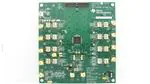
Figure 2. ADS5295EVM Basic Configuration
1. The EVM basic configuration uses the onboard single-ended clock as the default option. See
Section 9.2 for the ADC clock, various-mode jumper settings.
2. P1 or TP_VP & TP2: +5-V power supply.
3. JP4, JP5, and JP6 are set to enable +3.3V analog, +1.8VD digital, and +1.8VA analog to device,
respectively.
4. JP13: Enable onboard CMOS clock.
5. JP16, JP18, JP19, JP20: ADC clock source selection jumpers.
4
ADS5295, 8-Channel, Analog-to-Digital Converter Evaluation Module
Copyright © 2012, Texas Instruments Incorporated
SLAU442 – November 2012
Submit Documentation Feedback
�Software Installation and Operation
www.ti.com
3
Software Installation and Operation
The EVM requires a software installation to invoke the GUI. In addition, the TSW1400 High Speed Data
Converter Pro GUI (version 2.0 or higher) must be installed. The following section describes the
installation procedure for the ADS5295 GUI. For instructions on installing the TSW1400 High Speed Data
Converter Pro GUI, please visit the TI website.
3.1
GUI Installation – Mandatory
•
Unzip the installer file found on the TI website. Install the GUI by running setup.exe as administrator.
SLAU442 – November 2012
Submit Documentation Feedback
ADS5295, 8-Channel, Analog-to-Digital Converter Evaluation Module
Copyright © 2012, Texas Instruments Incorporated
5
�Software Installation and Operation
•
6
www.ti.com
Click Next.
ADS5295, 8-Channel, Analog-to-Digital Converter Evaluation Module
Copyright © 2012, Texas Instruments Incorporated
SLAU442 – November 2012
Submit Documentation Feedback
�Software Installation and Operation
www.ti.com
•
Click Next to proceed with the default install paths or Browse to desired paths and then click Next.
SLAU442 – November 2012
Submit Documentation Feedback
ADS5295, 8-Channel, Analog-to-Digital Converter Evaluation Module
Copyright © 2012, Texas Instruments Incorporated
7
�Software Installation and Operation
•
8
www.ti.com
Read the Software License Agreement and click I accept... and then click Next.
ADS5295, 8-Channel, Analog-to-Digital Converter Evaluation Module
Copyright © 2012, Texas Instruments Incorporated
SLAU442 – November 2012
Submit Documentation Feedback
�Software Installation and Operation
www.ti.com
•
Click Next to begin installation of listed components.
SLAU442 – November 2012
Submit Documentation Feedback
ADS5295, 8-Channel, Analog-to-Digital Converter Evaluation Module
Copyright © 2012, Texas Instruments Incorporated
9
�Software Installation and Operation
•
10
www.ti.com
The following window shows the installation progress:
ADS5295, 8-Channel, Analog-to-Digital Converter Evaluation Module
Copyright © 2012, Texas Instruments Incorporated
SLAU442 – November 2012
Submit Documentation Feedback
�Software Installation and Operation
www.ti.com
•
Clicking Finish completes the installation.
•
The PC must be restarted to complete the installation.
SLAU442 – November 2012
Submit Documentation Feedback
ADS5295, 8-Channel, Analog-to-Digital Converter Evaluation Module
Copyright © 2012, Texas Instruments Incorporated
11
�Test Setup
4
www.ti.com
Test Setup
To evaluate the ADS5295 device, a TSW1400EVM is required. Figure 3 shows the exact setup of these
two boards and external connectors.
• Connect the P10 connector of the ADS5295EVM to the J3 connector of the TSW1400EVM.
• Connect a +5-V supply at the P1 connector or across the TP_VP (+5 V) and TP2 (GND).
• Connect a +5-V wall adapter to the TSW1400EVM at the J12 connector.
• Connect a USB cable from the PC to USB1 on the ADS5295EVM.
• Connect a USB cable from the PC to USB port J5 of the TSW1400EVM.
• An external sampling clock is not required as the onboard 80-MHz CMOS clock oscillator is used in the
default configuration.
Figure 3. Hardware Setup of TSW1400EVM and ADS5295EVM
12
ADS5295, 8-Channel, Analog-to-Digital Converter Evaluation Module
Copyright © 2012, Texas Instruments Incorporated
SLAU442 – November 2012
Submit Documentation Feedback
�Power Up ADS5295
www.ti.com
5
Power Up ADS5295
After connecting the EVM to the TSW1400 using the P10 connector, the +5-V adapter to TSW1400EVM,
and the +5-V supply (from the external power supply) across TP_VP and TP2, power up is complete. One
green LED (LED_+5V) and one orange LED (LED33VA) should turn on as shown in Figure 4 (also see
Figure 20).
Figure 4. Power-Up Indications
SLAU442 – November 2012
Submit Documentation Feedback
ADS5295, 8-Channel, Analog-to-Digital Converter Evaluation Module
Copyright © 2012, Texas Instruments Incorporated
13
�Launch TSW1400 High Speed Data Converter Pro GUI
6
www.ti.com
Launch TSW1400 High Speed Data Converter Pro GUI
Upon launching the High Speed Data Converter Pro software, the GUI automatically detects the
TSW1400EVM that is connected and reports its serial number as shown in Figure 5.
• Clicking OK connects to the board.
Figure 5. High Speed Data Converter Pro GUI Launch
14
ADS5295, 8-Channel, Analog-to-Digital Converter Evaluation Module
Copyright © 2012, Texas Instruments Incorporated
SLAU442 – November 2012
Submit Documentation Feedback
�Launch TSW1400 High Speed Data Converter Pro GUI
www.ti.com
•
In the upper left corner of the GUI, select ADS5295 in the drop down menu of Select ADC.
•
Click Yes to update the Firmware for the ADC.
SLAU442 – November 2012
Submit Documentation Feedback
ADS5295, 8-Channel, Analog-to-Digital Converter Evaluation Module
Copyright © 2012, Texas Instruments Incorporated
15
�Launch TSW1400 High Speed Data Converter Pro GUI
www.ti.com
•
The following window appears while the firmware is loading.
•
A new tab labeled ADS5295 GUI appears in the High Speed Data Converter Pro GUI as shown in
Figure 6. This tab allows control of the ADS5295 device.
Figure 6. ADS5295 GUI
16
ADS5295, 8-Channel, Analog-to-Digital Converter Evaluation Module
Copyright © 2012, Texas Instruments Incorporated
SLAU442 – November 2012
Submit Documentation Feedback
�ADS5295 GUI Plug-In Tab
www.ti.com
7
ADS5295 GUI Plug-In Tab
The third tab of the High Speed Data Converter Pro GUI labeled ADS5295 GUI contains all the serial
register programming of the ADS5295 device.
• The ADS5295 GUI tab contains two sub-tabs called Read Me First and High Level Test. The default
tab displayed is the Read Me First tab as shown in Figure 7
• A table of all operating modes that the device supports is shown in this tab. The device can be quickly
configured to any of the operating modes listed by selecting the appropriate Saved Sequence file
name once the Playback Sequence button is pushed. This button is located in the right side of the
GUI in the RECORD/PLAYBACK COMMAND SEQUENCE section. (Note: The FPGA firmware of the
TSW1400 capture card is automatically updated to match the operating mode selected.)
• Clicking the High Level Test tab accesses all serial registers.
Figure 7. ADS5295 GUI Plug-In Tab
•
•
•
The High Level Test tab contains five sub-tabs: Top Level, Test Pattern, Dig Sig Proc, Channel Filter,
IN/OUTP Map. The default tab is the Top Level tab as shown in Figure 8.
The Top Level tab contains four sections: OUTPUT INTERFACE MODES, GENERAL SETUP,
POWERDOWN MODES, CUSTOM READ/ WRITE.
To verify that communication with the ADS5295 is functioning properly, inside the POWERDOWN
MODES section, click the checkbox labeled PDN_COMPLETE. The DC current from the power supply
should drop to approximately 140 mA when this box is checked. Uncheck this box before continuing.
SLAU442 – November 2012
Submit Documentation Feedback
ADS5295, 8-Channel, Analog-to-Digital Converter Evaluation Module
Copyright © 2012, Texas Instruments Incorporated
17
�ADS5295 GUI Plug-In Tab
www.ti.com
Figure 8. Top Level Tab
•
•
18
The OUTPUT INTERFACE MODES section contains all serial registers associated with the LVDS data
output format. The FPGA firmware of the TSW1400 capture card is automatically updated when one of
these registers, such as DATA_RATE, is updated.
The CUSTOM WRITE/READ section allows manual programming of a serial register's data value given
it's address. In addition, the current data value of any serial register can be read from the device by
inputting it's address.
ADS5295, 8-Channel, Analog-to-Digital Converter Evaluation Module
Copyright © 2012, Texas Instruments Incorporated
SLAU442 – November 2012
Submit Documentation Feedback
�ADS5295 GUI Plug-In Tab
www.ti.com
SLAU442 – November 2012
Submit Documentation Feedback
ADS5295, 8-Channel, Analog-to-Digital Converter Evaluation Module
Copyright © 2012, Texas Instruments Incorporated
19
�Test ADS5295
8
www.ti.com
Test ADS5295
This section describes how to test the ADS5295 device in two ways: Time Domain and Single Tone.
8.1
Step 1: Time Domain
Time Domain test consists of applying a RAMP function to the ADC inputs, capturing, and verifying that
every ADC code is generated incrementally.
• Select Test Pattern tab.
• In the TEST PATTERN MODES section, select RAMP PATTERN in the Enable Pattern Mode drop
down menu. (Note: the RAMP PATTERN is applied internal to the device to all ADC channels
simultaneously.)
Figure 9. ADS5295 Time Domain Setup
20
ADS5295, 8-Channel, Analog-to-Digital Converter Evaluation Module
Copyright © 2012, Texas Instruments Incorporated
SLAU442 – November 2012
Submit Documentation Feedback
�Test ADS5295
www.ti.com
•
On the ADC tab of the High Speed Data Converter Pro GUI, select Time Domain from the Test
Selection drop down menu as shown in Figure 10.
Figure 10. Time Domain Test
•
•
Input the appropriate ADC Sampling Rate (80 MHz in the default configuration of ADS5295 EVM) .
Press the Capture button.
SLAU442 – November 2012
Submit Documentation Feedback
ADS5295, 8-Channel, Analog-to-Digital Converter Evaluation Module
Copyright © 2012, Texas Instruments Incorporated
21
�Test ADS5295
•
www.ti.com
A saw tooth ramp should be captured as shown below.
Figure 11. ADS5295 RAMP Test Pattern Capture
22
ADS5295, 8-Channel, Analog-to-Digital Converter Evaluation Module
Copyright © 2012, Texas Instruments Incorporated
SLAU442 – November 2012
Submit Documentation Feedback
�Test ADS5295
www.ti.com
•
Use the zoom functions provided in the High Speed Data Converter Pro GUI to verify that the captured
RAMP is correct.
Figure 12. Graph Zoom Functions
SLAU442 – November 2012
Submit Documentation Feedback
ADS5295, 8-Channel, Analog-to-Digital Converter Evaluation Module
Copyright © 2012, Texas Instruments Incorporated
23
�Test ADS5295
•
www.ti.com
Zoom in on the RAMP until it is clear that every subsequent sample is an increment in ADC code as
shown below.
Figure 13. ADS5295 RAMP Verification
24
ADS5295, 8-Channel, Analog-to-Digital Converter Evaluation Module
Copyright © 2012, Texas Instruments Incorporated
SLAU442 – November 2012
Submit Documentation Feedback
�Test ADS5295
www.ti.com
•
Repeat the above procedure for all eight ADC channels using the selection box shown in Figure 14.
Figure 14. ADC Channel Selection
SLAU442 – November 2012
Submit Documentation Feedback
ADS5295, 8-Channel, Analog-to-Digital Converter Evaluation Module
Copyright © 2012, Texas Instruments Incorporated
25
�Test ADS5295
8.2
www.ti.com
Step 2: Single Tone FFT
The Single Tone test consists of applying a sine wave from an external signal generator to an ADC input,
capturing, and analyzing performance.
• Disable the RAMP PATTERN by setting the Enable Pattern Mode to None.
Figure 15. Disable RAMP PATTERN
26
ADS5295, 8-Channel, Analog-to-Digital Converter Evaluation Module
Copyright © 2012, Texas Instruments Incorporated
SLAU442 – November 2012
Submit Documentation Feedback
�Test ADS5295
www.ti.com
•
•
•
Set the Test Selection to Single Tone.
Set the ADC Input Target Frequency to 1M (Note: the value automatically changes to the exact
coherent frequency once the Auto Calculation box is checked) .
Check the box labeled Auto Calculation of Coherent Frequencies.
Figure 16. Single Tone Test
SLAU442 – November 2012
Submit Documentation Feedback
ADS5295, 8-Channel, Analog-to-Digital Converter Evaluation Module
Copyright © 2012, Texas Instruments Incorporated
27
�Test ADS5295
•
•
•
•
•
•
www.ti.com
Connect Channel 1 of the ADS5295EVM to a signal generator through a band-pass filter (BPF). If no
BPF is present, the results are not good.
The amplitude of the input signal is dependent on the insertion loss of the filter and cables used as
well as the desired backoff from full-scale. An iterative approach is used to determine the amplitude
setting required to operate at approximately -1.0 dBFS. In this test setup, the amplitude was set to
+18.4 dBm.
Set the frequency of the signal generator to that shown in the ADC Input Target Frequency box
(1.00219727M).
Change the window option to Hanning, due to the fact that input signal and onboard CMOS clock are
non-coherent.
Pressing the Capture button returns the test result.
Repeat for Channels 2 through 8.
Figure 17. Single Tone Capture
28
ADS5295, 8-Channel, Analog-to-Digital Converter Evaluation Module
Copyright © 2012, Texas Instruments Incorporated
SLAU442 – November 2012
Submit Documentation Feedback
�Board Configuration
www.ti.com
9
Board Configuration
9.1
Input/Output, Power Supply, and USB
Figure 18. I/O, PWR, and USB Connector
Table 1. Input/Output, Power, and USB
Connector
Description
J6,J7,J10….J15
Analog Input signals for Ch1-Ch8. Connect to a signal generator. A band-pass filter must be applied between
the generator and the SMA to get a better result.
J16
An alternative input for channel 8. Install two resistors (R169 and R170) and remove two resistors (R171 and
R172) from J6.
P1/TP_VP
P1 is the +5-V power supply connector. TP_VP is the test point for +5-V power supply.
JP4
Onboard 3.3-V Analog enables. Set up as shown in Figure 2 is required to use onboard 3.3 V.
JP5
Onboard 1.8-V Digital enables. Set up as shown in Figure 2 is required to use onboard 1.8 V.
JP6
Onboard 1.8-V Analog enables. Set up as shown in Figure 2 is required to use onboard 1.8 V.
SLAU442 – November 2012
Submit Documentation Feedback
ADS5295, 8-Channel, Analog-to-Digital Converter Evaluation Module
Copyright © 2012, Texas Instruments Incorporated
29
�Board Configuration
www.ti.com
Table 1. Input/Output, Power, and USB (continued)
Connector
Description
TP1, TP2, TP3,
TP4, TP5, TP14,
TP21, TP23,
TP25, TP34,
Ground test points.
USB1
USB interface connector
Table 2. Channel 8 Configuration
30
Input Interface Type
Connector
Description
Through Transformer
(Default)
J6
In default configuration, R171 and R172 are already populated
Through Amplifier (Not
Default)
J16
It is an alternative input for channel 8. Need to install two resistors (R169 and
R170) and remove two resistors(R171 and R172) from J6.It uses TI THS4509
single-ended to differential amplifier.
ADS5295, 8-Channel, Analog-to-Digital Converter Evaluation Module
Copyright © 2012, Texas Instruments Incorporated
SLAU442 – November 2012
Submit Documentation Feedback
�Board Configuration
www.ti.com
9.2
ADC Clock
Five options are available for the source of the ADC clocks. Refer to Table 3 for details. In Figure 19, the
EVM uses an onboard, single-ended clock as the default option.
Figure 19. ADS5295EVM Default Clock Jumper Locations
SLAU442 – November 2012
Submit Documentation Feedback
ADS5295, 8-Channel, Analog-to-Digital Converter Evaluation Module
Copyright © 2012, Texas Instruments Incorporated
31
�Board Configuration
www.ti.com
Table 3. ADC Clock Various Mode Jumper Settings
Reference
Designator
Jumper Setting
Diagram
Onboard CMOS
Oscillator
JP13, JP19, JP20,
JP16, JP18
JP13 (1-2), JP20 (2-3), JP19 (1-2), JP16 (2-3),
JP18 (2-3)
Dia. 1
(Default Option)
External CMOS
Clock Generator
J8, JP19, JP20, JP16, JP20 (2-3), JP19 (2-3), JP16 (2-3), JP18 (2-3)
JP18
and Connect CMOS clock generator output at
SMA connector J8.
Dia. 2
Transformer Based
External
JP15, JP17, JP16,
JP18, J4
JP15 (1-2), JP16 (1-2),JP17 (1-2), JP18 (1-2),
and Connect external Clock source at SMA
connector J4
Dia. 3
Onboard Clock
Buffer
(CDCLVP1102,U4)
JP13, JP19, JP20,
JP15, JP17, JP16,
JP18
JP13 (1-2), JP20 (1-2), JP19 (1-2), JP15 (2-3),
JP17 (2-3), JP16 (1-2), JP18 (1-2).
Dia. 4
Clock Type
Single Ended
Differential
Clock Signal
This configures the onboard CMOS oscillator
as clock input to buffer.
J8, JP19, JP20, JP15, JP19 (2-3), JP20 (1-2), JP15 (2-3), JP17 (2-3),
JP17, JP16, JP18
JP16 (1-2), JP18 (1-2) and Connect External
CMOS generator output at SMA connector J8.
Dia. 5
This configures the external CMOS source as
clock input to buffer.
Dia.1
Dia.2
Dia.4
32
ADS5295, 8-Channel, Analog-to-Digital Converter Evaluation Module
Copyright © 2012, Texas Instruments Incorporated
Dia.3
Dia.5
SLAU442 – November 2012
Submit Documentation Feedback
�Board Configuration
www.ti.com
9.3
Light-Emitting Diodes (LEDs)
Figure 20. ADS5295EVM LED Location
Table 4. LED Indicators
Reference Designator
Power Supply
Color
LED_+5V
+5 V
Green
LED1.8VA
+1.8 VA
Off
LED1.8VD
+1.8 VD
Off
LED3.3VA
+3.3 VA
Orange
SLAU442 – November 2012
Submit Documentation Feedback
ADS5295, 8-Channel, Analog-to-Digital Converter Evaluation Module
Copyright © 2012, Texas Instruments Incorporated
33
�Board Configuration
9.4
www.ti.com
Miscellaneous Test Points
Figure 21. ADS5295EVM Test Point Locations
Table 5. Miscellaneous Test Points
Reference Designator
34
Description
TP22
VCM: Common-mode output pin, 0.95-V output
TP6
CDC_VTH: Fixed voltage level (1.65 V)
TP_D0
SCLK: Serial clock input
TP_D1
SDA: Serial data input
TP_D2
SEN: Serial enable chip select
TP_D7
SDOUT: Serial data output
ADS5295, 8-Channel, Analog-to-Digital Converter Evaluation Module
Copyright © 2012, Texas Instruments Incorporated
SLAU442 – November 2012
Submit Documentation Feedback
�Board Configuration
www.ti.com
Table 5. Miscellaneous Test Points (continued)
Reference Designator
Description
JP14
RESET: Install to reset the device (DUT1) manually
JP12
PD: Install to power down the device (DUT1) manually
SLAU442 – November 2012
Submit Documentation Feedback
ADS5295, 8-Channel, Analog-to-Digital Converter Evaluation Module
Copyright © 2012, Texas Instruments Incorporated
35
�EVM Schematics
10
www.ti.com
EVM Schematics
Figure 22. Schematic, Sheet 1 of 9
36
ADS5295, 8-Channel, Analog-to-Digital Converter Evaluation Module
Copyright © 2012, Texas Instruments Incorporated
SLAU442 – November 2012
Submit Documentation Feedback
�EVM Schematics
www.ti.com
Figure 23. Schematic, Sheet 2 of 9
SLAU442 – November 2012
Submit Documentation Feedback
ADS5295, 8-Channel, Analog-to-Digital Converter Evaluation Module
Copyright © 2012, Texas Instruments Incorporated
37
�EVM Schematics
www.ti.com
Figure 24. Schematic, Sheet 3 of 9
38
ADS5295, 8-Channel, Analog-to-Digital Converter Evaluation Module
Copyright © 2012, Texas Instruments Incorporated
SLAU442 – November 2012
Submit Documentation Feedback
�EVM Schematics
www.ti.com
Figure 25. Schematic, Sheet 4 of 9
SLAU442 – November 2012
Submit Documentation Feedback
ADS5295, 8-Channel, Analog-to-Digital Converter Evaluation Module
Copyright © 2012, Texas Instruments Incorporated
39
�EVM Schematics
www.ti.com
Figure 26. Schematic, Sheet 5 of 9
40
ADS5295, 8-Channel, Analog-to-Digital Converter Evaluation Module
Copyright © 2012, Texas Instruments Incorporated
SLAU442 – November 2012
Submit Documentation Feedback
�EVM Schematics
www.ti.com
Figure 27. Schematic, Sheet 6 of 9
SLAU442 – November 2012
Submit Documentation Feedback
ADS5295, 8-Channel, Analog-to-Digital Converter Evaluation Module
Copyright © 2012, Texas Instruments Incorporated
41
�EVM Schematics
www.ti.com
Figure 28. Schematic, Sheet 7 of 9
42
ADS5295, 8-Channel, Analog-to-Digital Converter Evaluation Module
Copyright © 2012, Texas Instruments Incorporated
SLAU442 – November 2012
Submit Documentation Feedback
�EVM Schematics
www.ti.com
Figure 29. Schematic, Sheet 8 of 9
SLAU442 – November 2012
Submit Documentation Feedback
ADS5295, 8-Channel, Analog-to-Digital Converter Evaluation Module
Copyright © 2012, Texas Instruments Incorporated
43
�EVM Schematics
www.ti.com
Figure 30. Schematic, Sheet 9 of 9
44
ADS5295, 8-Channel, Analog-to-Digital Converter Evaluation Module
Copyright © 2012, Texas Instruments Incorporated
SLAU442 – November 2012
Submit Documentation Feedback
�ADS5295EVM Bill of Materials
www.ti.com
11
ADS5295EVM Bill of Materials
Table 6. Bill of Materials
ITEM
QTY
MFR P/N
Description
Value
MFR
RoH
S
REF DES
Digi-Key P/N
1
1
ADS5295IPFP
12-Bit 8-Channel ADC
ADS5295
Texas Instruments
Yes
DUT1
Texas Instruments
2
0
ADS5294IPFP
14-Bit 8-Channel ADC
ADS5294
Texas Instruments
Yes
DUT1
Texas Instruments
3
0
ADS5292IPFP
12-Bit 8-Channel ADC
ADS5292
Texas Instruments
Yes
DUT1
Texas Instruments
4
17
ADT4-1WT+
RF TRANSFORMER WIDEBAND, 2-775 MHz, 50 OHM
ADT4-1WT+
Mini-Circuits
Yes
T1-T17
Mini-Circuits
5
1
CDCLVP1102RGT
TWO LVPECL OUTPUT CLOCK BUFFER
CDCLVP1102
Texas Instruments
Yes
U4
296-25283-1-ND
6
2
CRCW06034R99FKEA
RES 4.99 OHM 1/10W 1% 0603 SMD
4.99 Ω
Vishay/Dale
Yes
R37,R38
541-4.99HHCT-ND
7
16
CRCW040210R0FKED
RES 10.0 OHM 1/16W 1% 0402 SMD
10.0 Ω
Vishay/Dale
Yes
R45,R46,R51,R52,R57,R58,R63,R64,R69,R70,
R75,R76,R81,R82, R87,R88
541-10.0LCT-ND
8
1
CRCW040249R9FKED
RES 49.9 OHM 1/16W 1% 0402 SMD
49.9 Ω
Vishay/Dale
Yes
R34
541-49.9LCT-ND
9
2
CRCW060353R6FKEA
RES 53.6 OHM 1/10W 1% 0603 SMD
53.6 Ω
Vishay/Dale
Yes
R31,R40
541-53.6HCT-ND
10
1
CRCW06030000Z0EA
RES 0.0 OHM 1/10W 0603 SMD
0.0 Ω
Vishay/Dale
Yes
R36
541-0.0GCT-ND
11
2
CRCW0603487RFKEA
RES 487 OHM 1/10W 1% 0603 SMD
487 Ω
Vishay/Dale
Yes
R32,R35
541-487HCT-ND
12
4
CRCW0402100RFKED
RES 100 OHM 1/16W 1% 0402 SMD
100 Ω
Vishay/Dale
Yes
R3,R4,R21,R22
541-100LCT-ND
13
3
CRCW04021K00FKED
RES 1.00K OHM 1/16W 1% 0402 SMD
1.00K Ω
Vishay/Dale
Yes
R2,R12,R168
541-1.00KLCT-ND
14
2
CRCW0402499RFKED
RES 499 OHM 1/16W 1% 0402 SMD
499 Ω
Vishay/Dale
Yes
R33,R164
541-499LCT-ND
15
3
CRCW080510K0FKEA
RES 10.0K OHM 1/8W 1% 0805 SMD
10.0K Ω
Vishay/Dale
Yes
R11,R13,R14
541-10.0KCCT-ND
16
7
C0402C104K8PACTU
CAP .10UF 10V CERAMIC X5R 0402
0.1uF
Kemet
Yes
C36,C37,C40,C41,C44,C45,C48
399-3027-1-ND
17
1
ECJ-0EB1H102K
CAPACITOR,SMT,0402,CER,1000pF,50V,10%,X7R
1000pF
Panasonic
Yes
C55
PCC1721CT-ND
18
4
ECJ-0EB1H122K
CAPACITOR,SMT,0402,CER,1200pF,50V,10%,X7R
1200pF
Panasonic
Yes
C71,C72,C75,C76
PCC1722CT-ND
19
2
ECJ-0EB1E181K
CAP 180PF 25V CERAMIC X7R 0402
180pF
Panasonic
Yes
C73,C74
PCC1705CT-ND
20
2
ECJ-0EC1H390J
CAP 39PF 50V CERAMIC 0402 SMD
39pF
Panasonic
Yes
C29,C30
PCC390CQCT-ND
21
5
ECJ-1V41E105M
CAP 1UF 25V CERAMIC 0603 X5S
1uF
Panasonic - ECG
Yes
C26,C31,C52,C68,C70
PCC2354CT-ND
22
1
ECS-3953M-800-BN
OSC,SMT,3.3V,50ppm,-40~85C,5nS,80.000 MHz
OSC 80 MHZ
ECS Inc
Yes
U3
XC344CT-ND
23
4
ELJ-RE33NGFA
INDUCTOR 33NH 2% 0603 SMD
33nH
Panasonic
Yes
L1,L4
PCD2008CT-ND
24
2
ERJ-2GEJ131
RESISTOR,SMT,0402,THICK FILM,5%,1/16W,130
130 Ω
Panasonic
Yes
R27,R29
P130JCT-ND
25
2
ERJ-2GEJ820
RESISTOR,SMT,0402,THICK FILM,5%,1/16W,82
82 Ω
Panasonic
Yes
R28,R30
P82JCT-ND
26
27
ERJ-2GE0R00X
RESISTOR/JUMPER,SMT,0402,0 OHM,5%,1/16W
0Ω
Panasonic
Yes
R5,R6,R7,R8,R10,R47,R48,R53,R54,R59,R60,
R65,R66,R71,R72,R77,R78,R83,R84,R89,R90,
R93,R166,R167,R171,R172,R173
P0.0JCT-ND
27
16
ERJ-2RKF24R9X
RESISTOR,SMT,0402,24.9 OHM,1%,1/16W
24.9 Ω
Panasonic
Yes
R43,R44,R49,R50,R55,R56,R61,R62,R67,R68,
R73,R74,R79,R80,R85,R86
P24.9LCT-ND
28
2
ERJ-2RKF49R9X
RESISTOR,SMT,0402,49.9 OHM,1%,1/16W
49.9 Ω
Panasonic
Yes
R1,R20
P49.9LCT-ND
29
3
ERJ-2RKF1000X
RESISTOR,SMT,0402,100 OHM,1%,1/10W
100 Ω
Panasonic
Yes
R15,R16, R18
P100LCT-ND
30
1
ERJ-2RKF3320X
RESISTOR,SMT,0402,332 OHM,1%,1/16W
332 Ω
Panasonic
Yes
R17
P332LCT-ND
31
1
FT245RL
USB FIFO IC INCORPORATE FTDICHIP-ID SECURITY
DONGLE
USB
FTDI
Yes
U10
768-1011-1-ND
32
0
GRM1555C1H3R3CZ0
1D
CAP CER 3.3PF 50V C0G 0402
3.3pF
Murata
Yes
C77,C85,C92,C99,C106,C113,C120,C127,C134
490-1270-1-ND
33
9
GRM1555C1H6R8DZ0
1D
CAP CER 6.8PF 50V C0G 0402
6.8pF
Murata
Yes
C77,C85,C92,C99,C106,C113,C120,C127,C134
490-1276-1-ND
SLAU442 – November 2012
Submit Documentation Feedback
ADS5295, 8-Channel, Analog-to-Digital Converter Evaluation Module
Copyright © 2012, Texas Instruments Incorporated
45
�ADS5295EVM Bill of Materials
www.ti.com
Table 6. Bill of Materials (continued)
ITEM
QTY
MFR P/N
Description
Value
MFR
RoH
S
REF DES
Digi-Key P/N
34
8
HI0805R800R-10
FERRITE CHIP POWER 80 OHM SMD
FERRITE
Laird-Signal Integrity
Products
Yes
FB1,FB2,FB3,FB4,FB5,FB6,FB7,FB8
240-2395-1-ND
35
2
ISO7240MDW
QUAD DIGITAL ISOLATORS
IC DGTL ISOL
Texas Instruments
Yes
U9,U11
296-22629-5-ND
36
3
JMK107BJ106MA-T
CAPACITOR,SMT,0603,CERAMIC,10uF,6.3V,20%,X5R
10uF
Taiyo Yuden
Yes
C33,C51,C54
587-1256-1-ND
37
10
JUMPER-0603(UN)
UNINSTALLED JUMPER,SMT0603
DNI
TP8,TP9,TP10,TP11,TP15,TP16,TP17,TP18,
TP19,TP20
DNI
38
3
LNJ308G8PRA
LED,SMT,0603,PURE GREEN,2.03V
LED
Panasonic
Yes
LED18VA,LED18VD,LED_+5V
P11485CT-ND
39
1
LNJ808R8ERA
LED,SMT,0603,ORANGE,1.8V
LED
Panasonic
Yes
LED33VA
P523CT-ND
40
1
897-43-005-00-100001
CONN RECEPT MINI-USB TYPE B SMT
USB Mini B
Mill-Max
Yes
USB1
ED90341CT-ND
41
1
QTH-060-01-L-D-A
HEADER,SMT,120P,0.5mm,FEM,2BANK,RECEPTACLE,168/19
8H
CONN
Samtec Inc
Yes
P10
SAM8189-ND
42
2
TEST POINT YELLOW
NOT INSTALLED
DNI
TP22, TP35
DNI
43
1
THS4509QRGTRQ1
WIDEBAND,LOW NOISE,LOW DISTORTION FULLY DIFF
AMP,1900 MHz
IC OPAMP
Texas Instruments
Yes
U12
296-24104-1-ND
44
9
TPSC226K016R0375
10%, 16V, 22uF
22µF
AVX
Yes
C35,C38,C39,C42,C43,C46,C47,C78,C79
478-1762-1-ND
45
2
TPS79618DCQR
ULTRALOW-NOISE HI PSRR FAST RF 1-A LDO LINEAR
REGULATOR,1.8V
LDO REG 1.8V
Texas Instruments
Yes
U6,U7
296-13762-1-ND
46
1
TPS79633DCQR
ULTRALOW-NOISE HI PSRR FAST RF 1-A LDO LINEAR
REGULATOR,3.3V
LDO REG 3.3V
Texas Instruments
Yes
U8
296-13766-1-ND
47
1
1SMB5921BT3G
DIODE ZENER 6.8V 3W SMB
DIODE Zener
ON Semiconductor
Yes
Z1
1SMB5921BT3GOSCT-ND
48
5
9-146285-0-02
CONN HEADR BRKWAY .100 02POS STR
CONN Header
TE Connectivity
Yes
JP10,JP11,JP12,JP13,JP14
A32700-02-ND
49
10
9-146285-0-03
CONN HEADR BRKWAY .100 03POS STR
CONN Header
TE Connectivity
Yes
JP4,JP5,JP6,JP15,JP16,JP17,JP18,JP19,JP20,J
P21
A32700-03-ND
50
12
901-144-8
SMA COAX STRAIGHT PCB CURRENT P/N IS 901-144-8RFX
SMA
Amphenol
Yes
J4,J5,J6,J7,J8,J10,J11,J12,J13,J14,J15,J16
ARFX1231-ND
51
76
0402YD104KAT2A
CAP CERM .1UF 10% 16V X5R 0402
0.1uF
AVX
Yes
C1,C2,C3,C4,C5,C6,C7,C8,C13,C14,C17,C25,
C27,C28,C32,C34,C53,C56,C57,C58,C62,C63,
C65,C66,C67,C69,C81,C82,C83,C84,C86,C87,
C88,C89,C90,C91,C93,C94,C95,C96,C97,C98,
C100,C101,C102,C103,C104,C105,C107,C108,
C109,C110,C111,C112,C114,C115,C116,C117,
C118,C119,C121,C122,C123,C124,C125,C126,
C128,C129,C130,C131,C132,C133,C135,C136,
C137,C138
478-1126-1-ND
52
1
5000
TESTPOINT,THU,MINIATURE,0.1LS,120TL, RED
Test Point,Red
Keystone Electronics
Yes
TP_VP
5000K-ND
53
9
5001
TESTPOINT,THU,MINIATURE,0.1LS,120TL, BLACK
Test Point,Black
Keystone Electronics
Yes
TP1,TP2,TP3,TP4,TP5,TP14,TP21,TP23,TP25
5001K-ND
54
5
5002
TESTPOINT,THU,MINIATURE,0.1LS,120TL, WHITE
Test Point,White
Keystone Electronics
Yes
TP6,TP_D0, TP_D1,TP_D2,TP_D7
5002K-ND
55
1
5003
TESTPOINT,THU,MINIATURE,0.1LS,120TL, ORANGE
Test Point,Orange
Keystone Electronics
Yes
TP34
5003K-ND
56
1
39357-0002
HEADER, THRU, POWER, 2P,3.5MM, EUROSTYLE
CONN TERMINAL
Molex Connector Corp
Yes
P1
WM7877-ND
57
0
CRCW06030000Z0EA
RES 0.0 OHM 1/10W 0603 SMD
0.0 Ω
Vishay/Dale
Yes
R169, R170,R201, R202
541-0.0GCT-ND (DNI)
58
4
24436
STANDOFF HEX M3 THR ALUM 18MM
STANDOFF
Keystone
Yes
STANDOFF HEX M3 THR ALUM 18MM
24436K-ND
59
4
29311
SCREW STEEL M3 THR 6MM
SCREW
Keystone
Yes
SCREW STEEL M3 THR 6MM
29311K-ND
46
ADS5295, 8-Channel, Analog-to-Digital Converter Evaluation Module
Copyright © 2012, Texas Instruments Incorporated
SLAU442 – November 2012
Submit Documentation Feedback
�ADS5295EVM Printed-Circuit Board Layout
www.ti.com
12
ADS5295EVM Printed-Circuit Board Layout
Figure 31 through Figure 42 illustrate the PCB layouts for the EVM.
Figure 31. ADS5295EVM Top Layer Assembly Drawing – Top View
SLAU442 – November 2012
Submit Documentation Feedback
ADS5295, 8-Channel, Analog-to-Digital Converter Evaluation Module
Copyright © 2012, Texas Instruments Incorporated
47
�ADS5295EVM Printed-Circuit Board Layout
www.ti.com
Figure 32. ADS5295EVM Bottom Layer Assembly Drawing – Bottom View
48
ADS5295, 8-Channel, Analog-to-Digital Converter Evaluation Module
Copyright © 2012, Texas Instruments Incorporated
SLAU442 – November 2012
Submit Documentation Feedback
�www.ti.com
ADS5295EVM Printed-Circuit Board Layout
Figure 33. ADS5295EVM Solder Paste Top
SLAU442 – November 2012
Submit Documentation Feedback
ADS5295, 8-Channel, Analog-to-Digital Converter Evaluation Module
Copyright © 2012, Texas Instruments Incorporated
49
�ADS5295EVM Printed-Circuit Board Layout
www.ti.com
Figure 34. ADS5295EVM Solder Paste Bottom
50
ADS5295, 8-Channel, Analog-to-Digital Converter Evaluation Module
Copyright © 2012, Texas Instruments Incorporated
SLAU442 – November 2012
Submit Documentation Feedback
�www.ti.com
ADS5295EVM Printed-Circuit Board Layout
Figure 35. ADS5295EVM Soldermask Top
SLAU442 – November 2012
Submit Documentation Feedback
ADS5295, 8-Channel, Analog-to-Digital Converter Evaluation Module
Copyright © 2012, Texas Instruments Incorporated
51
�ADS5295EVM Printed-Circuit Board Layout
www.ti.com
Figure 36. ADS5295EVM Soldermask Bottom
52
ADS5295, 8-Channel, Analog-to-Digital Converter Evaluation Module
Copyright © 2012, Texas Instruments Incorporated
SLAU442 – November 2012
Submit Documentation Feedback
�ADS5295EVM Printed-Circuit Board Layout
www.ti.com
Figure 37. ADS5295EVM Bottom Layer Copper – Bottom View
SLAU442 – November 2012
Submit Documentation Feedback
ADS5295, 8-Channel, Analog-to-Digital Converter Evaluation Module
Copyright © 2012, Texas Instruments Incorporated
53
�ADS5295EVM Printed-Circuit Board Layout
www.ti.com
Figure 38. ADS5295EVM Layer 5 Ground Plane
54
ADS5295, 8-Channel, Analog-to-Digital Converter Evaluation Module
Copyright © 2012, Texas Instruments Incorporated
SLAU442 – November 2012
Submit Documentation Feedback
�www.ti.com
ADS5295EVM Printed-Circuit Board Layout
Figure 39. ADS5295EVM Layer 4 Split Power Planes
SLAU442 – November 2012
Submit Documentation Feedback
ADS5295, 8-Channel, Analog-to-Digital Converter Evaluation Module
Copyright © 2012, Texas Instruments Incorporated
55
�ADS5295EVM Printed-Circuit Board Layout
www.ti.com
Figure 40. ADS5295EVM Layer 3 Split Power Planes
56
ADS5295, 8-Channel, Analog-to-Digital Converter Evaluation Module
Copyright © 2012, Texas Instruments Incorporated
SLAU442 – November 2012
Submit Documentation Feedback
�www.ti.com
ADS5295EVM Printed-Circuit Board Layout
Figure 41. ADS5295EVM Layer 2 Ground Plane
SLAU442 – November 2012
Submit Documentation Feedback
ADS5295, 8-Channel, Analog-to-Digital Converter Evaluation Module
Copyright © 2012, Texas Instruments Incorporated
57
�ADS5295EVM Printed-Circuit Board Layout
www.ti.com
Figure 42. ADS5295EVM Top Layer Copper – Top View
58
ADS5295, 8-Channel, Analog-to-Digital Converter Evaluation Module
Copyright © 2012, Texas Instruments Incorporated
SLAU442 – November 2012
Submit Documentation Feedback
�EVALUATION BOARD/KIT/MODULE (EVM) ADDITIONAL TERMS
Texas Instruments (TI) provides the enclosed Evaluation Board/Kit/Module (EVM) under the following conditions:
The user assumes all responsibility and liability for proper and safe handling of the goods. Further, the user indemnifies TI from all claims
arising from the handling or use of the goods.
Should this evaluation board/kit not meet the specifications indicated in the User’s Guide, the board/kit may be returned within 30 days from
the date of delivery for a full refund. THE FOREGOING LIMITED WARRANTY IS THE EXCLUSIVE WARRANTY MADE BY SELLER TO
BUYER AND IS IN LIEU OF ALL OTHER WARRANTIES, EXPRESSED, IMPLIED, OR STATUTORY, INCLUDING ANY WARRANTY OF
MERCHANTABILITY OR FITNESS FOR ANY PARTICULAR PURPOSE. EXCEPT TO THE EXTENT OF THE INDEMNITY SET FORTH
ABOVE, NEITHER PARTY SHALL BE LIABLE TO THE OTHER FOR ANY INDIRECT, SPECIAL, INCIDENTAL, OR CONSEQUENTIAL
DAMAGES.
Please read the User's Guide and, specifically, the Warnings and Restrictions notice in the User's Guide prior to handling the product. This
notice contains important safety information about temperatures and voltages. For additional information on TI's environmental and/or safety
programs, please visit www.ti.com/esh or contact TI.
No license is granted under any patent right or other intellectual property right of TI covering or relating to any machine, process, or
combination in which such TI products or services might be or are used. TI currently deals with a variety of customers for products, and
therefore our arrangement with the user is not exclusive. TI assumes no liability for applications assistance, customer product design,
software performance, or infringement of patents or services described herein.
REGULATORY COMPLIANCE INFORMATION
As noted in the EVM User’s Guide and/or EVM itself, this EVM and/or accompanying hardware may or may not be subject to the Federal
Communications Commission (FCC) and Industry Canada (IC) rules.
For EVMs not subject to the above rules, this evaluation board/kit/module is intended for use for ENGINEERING DEVELOPMENT,
DEMONSTRATION OR EVALUATION PURPOSES ONLY and is not considered by TI to be a finished end product fit for general consumer
use. It generates, uses, and can radiate radio frequency energy and has not been tested for compliance with the limits of computing
devices pursuant to part 15 of FCC or ICES-003 rules, which are designed to provide reasonable protection against radio frequency
interference. Operation of the equipment may cause interference with radio communications, in which case the user at his own expense will
be required to take whatever measures may be required to correct this interference.
General Statement for EVMs including a radio
User Power/Frequency Use Obligations: This radio is intended for development/professional use only in legally allocated frequency and
power limits. Any use of radio frequencies and/or power availability of this EVM and its development application(s) must comply with local
laws governing radio spectrum allocation and power limits for this evaluation module. It is the user’s sole responsibility to only operate this
radio in legally acceptable frequency space and within legally mandated power limitations. Any exceptions to this are strictly prohibited and
unauthorized by Texas Instruments unless user has obtained appropriate experimental/development licenses from local regulatory
authorities, which is responsibility of user including its acceptable authorization.
For EVMs annotated as FCC – FEDERAL COMMUNICATIONS COMMISSION Part 15 Compliant
Caution
This device complies with part 15 of the FCC Rules. Operation is subject to the following two conditions: (1) This device may not cause
harmful interference, and (2) this device must accept any interference received, including interference that may cause undesired operation.
Changes or modifications not expressly approved by the party responsible for compliance could void the user's authority to operate the
equipment.
FCC Interference Statement for Class A EVM devices
This equipment has been tested and found to comply with the limits for a Class A digital device, pursuant to part 15 of the FCC Rules.
These limits are designed to provide reasonable protection against harmful interference when the equipment is operated in a commercial
environment. This equipment generates, uses, and can radiate radio frequency energy and, if not installed and used in accordance with the
instruction manual, may cause harmful interference to radio communications. Operation of this equipment in a residential area is likely to
cause harmful interference in which case the user will be required to correct the interference at his own expense.
�FCC Interference Statement for Class B EVM devices
This equipment has been tested and found to comply with the limits for a Class B digital device, pursuant to part 15 of the FCC Rules.
These limits are designed to provide reasonable protection against harmful interference in a residential installation. This equipment
generates, uses and can radiate radio frequency energy and, if not installed and used in accordance with the instructions, may cause
harmful interference to radio communications. However, there is no guarantee that interference will not occur in a particular installation. If
this equipment does cause harmful interference to radio or television reception, which can be determined by turning the equipment off and
on, the user is encouraged to try to correct the interference by one or more of the following measures:
• Reorient or relocate the receiving antenna.
• Increase the separation between the equipment and receiver.
• Connect the equipment into an outlet on a circuit different from that to which the receiver is connected.
• Consult the dealer or an experienced radio/TV technician for help.
For EVMs annotated as IC – INDUSTRY CANADA Compliant
This Class A or B digital apparatus complies with Canadian ICES-003.
Changes or modifications not expressly approved by the party responsible for compliance could void the user’s authority to operate the
equipment.
Concerning EVMs including radio transmitters
This device complies with Industry Canada licence-exempt RSS standard(s). Operation is subject to the following two conditions: (1) this
device may not cause interference, and (2) this device must accept any interference, including interference that may cause undesired
operation of the device.
Concerning EVMs including detachable antennas
Under Industry Canada regulations, this radio transmitter may only operate using an antenna of a type and maximum (or lesser) gain
approved for the transmitter by Industry Canada. To reduce potential radio interference to other users, the antenna type and its gain should
be so chosen that the equivalent isotropically radiated power (e.i.r.p.) is not more than that necessary for successful communication.
This radio transmitter has been approved by Industry Canada to operate with the antenna types listed in the user guide with the maximum
permissible gain and required antenna impedance for each antenna type indicated. Antenna types not included in this list, having a gain
greater than the maximum gain indicated for that type, are strictly prohibited for use with this device.
Cet appareil numérique de la classe A ou B est conforme à la norme NMB-003 du Canada.
Les changements ou les modifications pas expressément approuvés par la partie responsable de la conformité ont pu vider l’autorité de
l'utilisateur pour actionner l'équipement.
Concernant les EVMs avec appareils radio
Le présent appareil est conforme aux CNR d'Industrie Canada applicables aux appareils radio exempts de licence. L'exploitation est
autorisée aux deux conditions suivantes : (1) l'appareil ne doit pas produire de brouillage, et (2) l'utilisateur de l'appareil doit accepter tout
brouillage radioélectrique subi, même si le brouillage est susceptible d'en compromettre le fonctionnement.
Concernant les EVMs avec antennes détachables
Conformément à la réglementation d'Industrie Canada, le présent émetteur radio peut fonctionner avec une antenne d'un type et d'un gain
maximal (ou inférieur) approuvé pour l'émetteur par Industrie Canada. Dans le but de réduire les risques de brouillage radioélectrique à
l'intention des autres utilisateurs, il faut choisir le type d'antenne et son gain de sorte que la puissance isotrope rayonnée équivalente
(p.i.r.e.) ne dépasse pas l'intensité nécessaire à l'établissement d'une communication satisfaisante.
Le présent émetteur radio a été approuvé par Industrie Canada pour fonctionner avec les types d'antenne énumérés dans le manuel
d’usage et ayant un gain admissible maximal et l'impédance requise pour chaque type d'antenne. Les types d'antenne non inclus dans
cette liste, ou dont le gain est supérieur au gain maximal indiqué, sont strictement interdits pour l'exploitation de l'émetteur.
SPACER
SPACER
SPACER
SPACER
SPACER
SPACER
SPACER
SPACER
�【Important Notice for Users of this Product in Japan】
】
This development kit is NOT certified as Confirming to Technical Regulations of Radio Law of Japan
If you use this product in Japan, you are required by Radio Law of Japan to follow the instructions below with respect to this product:
1.
2.
3.
Use this product in a shielded room or any other test facility as defined in the notification #173 issued by Ministry of Internal Affairs and
Communications on March 28, 2006, based on Sub-section 1.1 of Article 6 of the Ministry’s Rule for Enforcement of Radio Law of
Japan,
Use this product only after you obtained the license of Test Radio Station as provided in Radio Law of Japan with respect to this
product, or
Use of this product only after you obtained the Technical Regulations Conformity Certification as provided in Radio Law of Japan with
respect to this product. Also, please do not transfer this product, unless you give the same notice above to the transferee. Please note
that if you could not follow the instructions above, you will be subject to penalties of Radio Law of Japan.
Texas Instruments Japan Limited
(address) 24-1, Nishi-Shinjuku 6 chome, Shinjuku-ku, Tokyo, Japan
http://www.tij.co.jp
【ご使用にあたっての注】
本開発キットは技術基準適合証明を受けておりません。
本製品のご使用に際しては、電波法遵守のため、以下のいずれかの措置を取っていただく必要がありますのでご注意ください。
1.
2.
3.
電波法施行規則第6条第1項第1号に基づく平成18年3月28日総務省告示第173号で定められた電波暗室等の試験設備でご使用いただく。
実験局の免許を取得後ご使用いただく。
技術基準適合証明を取得後ご使用いただく。
なお、本製品は、上記の「ご使用にあたっての注意」を譲渡先、移転先に通知しない限り、譲渡、移転できないものとします。
上記を遵守頂けない場合は、電波法の罰則が適用される可能性があることをご留意ください。
日本テキサス・インスツルメンツ株式会社
東京都新宿区西新宿6丁目24番1号
西新宿三井ビル
http://www.tij.co.jp
SPACER
SPACER
SPACER
SPACER
SPACER
SPACER
SPACER
SPACER
SPACER
SPACER
SPACER
SPACER
SPACER
SPACER
SPACER
SPACER
�EVALUATION BOARD/KIT/MODULE (EVM)
WARNINGS, RESTRICTIONS AND DISCLAIMERS
For Feasibility Evaluation Only, in Laboratory/Development Environments. Unless otherwise indicated, this EVM is not a finished
electrical equipment and not intended for consumer use. It is intended solely for use for preliminary feasibility evaluation in
laboratory/development environments by technically qualified electronics experts who are familiar with the dangers and application risks
associated with handling electrical mechanical components, systems and subsystems. It should not be used as all or part of a finished end
product.
Your Sole Responsibility and Risk. You acknowledge, represent and agree that:
1.
2.
3.
4.
You have unique knowledge concerning Federal, State and local regulatory requirements (including but not limited to Food and Drug
Administration regulations, if applicable) which relate to your products and which relate to your use (and/or that of your employees,
affiliates, contractors or designees) of the EVM for evaluation, testing and other purposes.
You have full and exclusive responsibility to assure the safety and compliance of your products with all such laws and other applicable
regulatory requirements, and also to assure the safety of any activities to be conducted by you and/or your employees, affiliates,
contractors or designees, using the EVM. Further, you are responsible to assure that any interfaces (electronic and/or mechanical)
between the EVM and any human body are designed with suitable isolation and means to safely limit accessible leakage currents to
minimize the risk of electrical shock hazard.
You will employ reasonable safeguards to ensure that your use of the EVM will not result in any property damage, injury or death, even
if the EVM should fail to perform as described or expected.
You will take care of proper disposal and recycling of the EVM’s electronic components and packing materials.
Certain Instructions. It is important to operate this EVM within TI’s recommended specifications and environmental considerations per the
user guidelines. Exceeding the specified EVM ratings (including but not limited to input and output voltage, current, power, and
environmental ranges) may cause property damage, personal injury or death. If there are questions concerning these ratings please contact
a TI field representative prior to connecting interface electronics including input power and intended loads. Any loads applied outside of the
specified output range may result in unintended and/or inaccurate operation and/or possible permanent damage to the EVM and/or
interface electronics. Please consult the EVM User's Guide prior to connecting any load to the EVM output. If there is uncertainty as to the
load specification, please contact a TI field representative. During normal operation, some circuit components may have case temperatures
greater than 60°C as long as the input and output are maintained at a normal ambient operating temperature. These components include
but are not limited to linear regulators, switching transistors, pass transistors, and current sense resistors which can be identified using the
EVM schematic located in the EVM User's Guide. When placing measurement probes near these devices during normal operation, please
be aware that these devices may be very warm to the touch. As with all electronic evaluation tools, only qualified personnel knowledgeable
in electronic measurement and diagnostics normally found in development environments should use these EVMs.
Agreement to Defend, Indemnify and Hold Harmless. You agree to defend, indemnify and hold TI, its licensors and their representatives
harmless from and against any and all claims, damages, losses, expenses, costs and liabilities (collectively, "Claims") arising out of or in
connection with any use of the EVM that is not in accordance with the terms of the agreement. This obligation shall apply whether Claims
arise under law of tort or contract or any other legal theory, and even if the EVM fails to perform as described or expected.
Safety-Critical or Life-Critical Applications. If you intend to evaluate the components for possible use in safety critical applications (such
as life support) where a failure of the TI product would reasonably be expected to cause severe personal injury or death, such as devices
which are classified as FDA Class III or similar classification, then you must specifically notify TI of such intent and enter into a separate
Assurance and Indemnity Agreement.
Mailing Address: Texas Instruments, Post Office Box 655303, Dallas, Texas 75265
Copyright © 2012, Texas Instruments Incorporated
�IMPORTANT NOTICE
Texas Instruments Incorporated and its subsidiaries (TI) reserve the right to make corrections, enhancements, improvements and other
changes to its semiconductor products and services per JESD46, latest issue, and to discontinue any product or service per JESD48, latest
issue. Buyers should obtain the latest relevant information before placing orders and should verify that such information is current and
complete. All semiconductor products (also referred to herein as “components”) are sold subject to TI’s terms and conditions of sale
supplied at the time of order acknowledgment.
TI warrants performance of its components to the specifications applicable at the time of sale, in accordance with the warranty in TI’s terms
and conditions of sale of semiconductor products. Testing and other quality control techniques are used to the extent TI deems necessary
to support this warranty. Except where mandated by applicable law, testing of all parameters of each component is not necessarily
performed.
TI assumes no liability for applications assistance or the design of Buyers’ products. Buyers are responsible for their products and
applications using TI components. To minimize the risks associated with Buyers’ products and applications, Buyers should provide
adequate design and operating safeguards.
TI does not warrant or represent that any license, either express or implied, is granted under any patent right, copyright, mask work right, or
other intellectual property right relating to any combination, machine, or process in which TI components or services are used. Information
published by TI regarding third-party products or services does not constitute a license to use such products or services or a warranty or
endorsement thereof. Use of such information may require a license from a third party under the patents or other intellectual property of the
third party, or a license from TI under the patents or other intellectual property of TI.
Reproduction of significant portions of TI information in TI data books or data sheets is permissible only if reproduction is without alteration
and is accompanied by all associated warranties, conditions, limitations, and notices. TI is not responsible or liable for such altered
documentation. Information of third parties may be subject to additional restrictions.
Resale of TI components or services with statements different from or beyond the parameters stated by TI for that component or service
voids all express and any implied warranties for the associated TI component or service and is an unfair and deceptive business practice.
TI is not responsible or liable for any such statements.
Buyer acknowledges and agrees that it is solely responsible for compliance with all legal, regulatory and safety-related requirements
concerning its products, and any use of TI components in its applications, notwithstanding any applications-related information or support
that may be provided by TI. Buyer represents and agrees that it has all the necessary expertise to create and implement safeguards which
anticipate dangerous consequences of failures, monitor failures and their consequences, lessen the likelihood of failures that might cause
harm and take appropriate remedial actions. Buyer will fully indemnify TI and its representatives against any damages arising out of the use
of any TI components in safety-critical applications.
In some cases, TI components may be promoted specifically to facilitate safety-related applications. With such components, TI’s goal is to
help enable customers to design and create their own end-product solutions that meet applicable functional safety standards and
requirements. Nonetheless, such components are subject to these terms.
No TI components are authorized for use in FDA Class III (or similar life-critical medical equipment) unless authorized officers of the parties
have executed a special agreement specifically governing such use.
Only those TI components which TI has specifically designated as military grade or “enhanced plastic” are designed and intended for use in
military/aerospace applications or environments. Buyer acknowledges and agrees that any military or aerospace use of TI components
which have not been so designated is solely at the Buyer's risk, and that Buyer is solely responsible for compliance with all legal and
regulatory requirements in connection with such use.
TI has specifically designated certain components as meeting ISO/TS16949 requirements, mainly for automotive use. In any case of use of
non-designated products, TI will not be responsible for any failure to meet ISO/TS16949.
Products
Applications
Audio
www.ti.com/audio
Automotive and Transportation
www.ti.com/automotive
Amplifiers
amplifier.ti.com
Communications and Telecom
www.ti.com/communications
Data Converters
dataconverter.ti.com
Computers and Peripherals
www.ti.com/computers
DLP® Products
www.dlp.com
Consumer Electronics
www.ti.com/consumer-apps
DSP
dsp.ti.com
Energy and Lighting
www.ti.com/energy
Clocks and Timers
www.ti.com/clocks
Industrial
www.ti.com/industrial
Interface
interface.ti.com
Medical
www.ti.com/medical
Logic
logic.ti.com
Security
www.ti.com/security
Power Mgmt
power.ti.com
Space, Avionics and Defense
www.ti.com/space-avionics-defense
Microcontrollers
microcontroller.ti.com
Video and Imaging
www.ti.com/video
RFID
www.ti-rfid.com
OMAP Applications Processors
www.ti.com/omap
TI E2E Community
e2e.ti.com
Wireless Connectivity
www.ti.com/wirelessconnectivity
Mailing Address: Texas Instruments, Post Office Box 655303, Dallas, Texas 75265
Copyright © 2012, Texas Instruments Incorporated
�