ADS5413
www.ti.com
SLWS153 − DECEMBER 2003
SINGLE 12-BIT, 65-MSPS IF SAMPLING
ANALOG-TO-DIGITAL CONVERTER
FEATURES
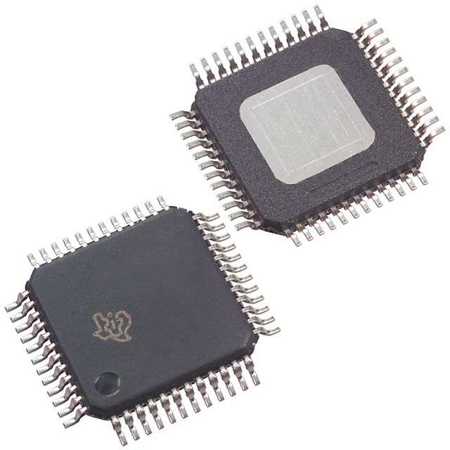
D 48-Pin TQFP Package With PowerPad
D
D
D
D
D
D
D
D
D
D 64.5-dBFS SNR and 72-dBc SFDR at 65 MSPS
(7 mm x 7 mm body size)
12-Bit Resolution
65-MSPS Maximum Sample Rate
and 190-MHz Input
D Power-Down Mode
D Single-Ended or Differential Clock
D 1-GHz −3-dB Input Bandwidth
2-Vpp Differential Input Range
3.3-V Single Supply Operation
1.8-V to 3.3-V Output Supply
400-mW Total Power Dissipation
APPLICATIONS
D High IF Sampling Receivers
D Medical Imaging
D Portable Instrumentation
Two’s Complement Output Format
On-Chip S/H and Duty Cycle Adjust Circuit
Internal or External Reference
DESCRIPTION
The ADS5413 is a low power, 12-bit, 65-MSPS, CMOS pipeline analog-to-digital converter (ADC) that operates from a
single 3.3-V supply, while offering the choice of digital output levels from 1.8 V to 3.3 V. The low noise, high linearity, and
low clock jitter makes the ADC well suited for high-input frequency sampling applications. On-chip duty cycle adjust circuit
allows the use of a non-50% duty cycle. This can be bypassed for applications requiring low jitter or asynchronous
sampling. The device can also be clocked with single ended or differential clock, without change in performance. The
internal reference can be bypassed to use an external reference to suit the accuracy and low drift requirements of the
application.
The device is specified over full temperature range (−40°C to +85°C).
FUNCTIONAL BLOCK DIAGRAM
AVDD
PWD
Gain
Stage
S/H
VINP
Gain
Stage
Σ
Σ
A/D
REF SEL
CML
VREFB
Flash
Σ
A/D
7 Stages
VINN
VREFT
Gain
Stage
OVDD
D/A
A/D
D/A
A/D
D/A
2.25 V
Internal
Reference
1.25 V Generator
1.8 V
2
VBG
2
2
2
Digital Error Correction
CLK
DCA
CLKC
DCA
D[0:11]
AGND
OGND
Please be aware that an important notice concerning availability, standard warranty, and use in critical applications of Texas Instruments
semiconductor products and disclaimers thereto appears at the end of this data sheet.
CommsADC is a trademark of Texas Instruments.
PRODUCTION DATA information is current as of publication date. Products
conform to specifications per the terms of Texas Instruments standard warranty.
Production processing does not necessarily include testing of all parameters.
Copyright 2003, Texas Instruments Incorporated
�ADS5413
www.ti.com
SLWS153 − DECEMBER 2003
These devices have limited built-in ESD protection. The leads should be shorted together or the device placed in conductive foam during
storage or handling to prevent electrostatic damage to the MOS gates.
PACKAGE/ORDERING INFORMATION(1)
(1)
(2)
PRODUCT
PACKAGE LEAD
PACKAGE
DESIGNATOR
SPECIFIED
TEMPERATURE
RANGE
PACKAGE
MARKING
ORDERING
NUMBER
TRANSPORT
MEDIA, QUANTITY
ADS5413
HTQFP-48(2)
PowerPAD
PHP
−40°C to 85°C
AZ5413
ADS5413IPHP
Tray, 250
For the most current product and ordering information, see the Package Option Addendum located at the end of this data sheet.
Thermal pad size: 3,5 mm × 3,5 mm
ABSOLUTE MAXIMUM RATINGS
over operating free-air temperature range unless otherwise noted(1)
UNITS
AVDD measured with respect to AGND
Supply voltage range
−0.3 V to 3.9 V
OVDD measure with respect to OGND
−0.3 V to 3.9 V
Digital input, measured with respect to AGND
−0.3 V to AVDD + 0.3 V
Reference inputs Vrefb or Vreft, measured with respect to AGND
−0.3 V to AVDD + 0.3 V
Analog inputs Vinp or Vinn, measured with respect to AGND
−0.3 V to AVDD + 0.3 V
Maximum storage temperature
150°C
Soldering reflow temperature
235°C
(1)
Stresses beyond those listed under “absolute maximum ratings” may cause permanent damage to the device. These are stress ratings only, and
functional operation of the device at these or any other conditions beyond those indicated under “recommended operating conditions” is not
implied. Exposure to absolute-maximum-rated conditions for extended periods may affect device reliability.
RECOMMENDED OPERATING CONDITIONS(1)
MIN
NOM
MAX
UNIT
ENVIRONMENTAL
Operating free-air temperature, TA
−40
85
°C
3.6
V
3.6
V
SUPPLIES
Analog supply voltage, V(AVDD)
Output driver supply voltage, V(OVDD)
3
3.3
1.6
ANALOG INPUTS
CML(2)
Input common-mode voltage
Differential input voltage range
V
2
VPP
CLOCK INPUTS, CLK AND CLKC
Sample rate, fS = 1/tc
5
Differential input swing (see Figure 17)
1
Differential input common-mode voltage (see Figure 18)
1.65
65
MHz
6
VPP
V
Clock pulse width high, tw(H) (see Figure 16, with DCA off)
6.92
ns
Clock pulse width low, tw(L) (see Figure 16, with DCA off)
6.92
ns
(1)
Recommended by design and characterization but not tested at final production unless specified under the electrical characteristics section.
(2) See V
(CML) in the internal reference generator section.
2
�ADS5413
www.ti.com
SLWS153 − DECEMBER 2003
ELECTRICAL CHARACTERISTICS
over operating free-air temperature range, clock frequency = 65 MSPS, 50% clock duty cycle (AVDD = OVDD = 3.3 V), duty cylce adjust off,
internal reference, AIN = −1 dBFS, 1.2-VPP square differential clock (unless otherwise noted)
PARAMETER
TEST CONDITIONS
MIN
TYP
MAX
UNIT
DC PERFORMANCE
Power Supply
Total analog supply current with internal
reference and DCA on
I(AVDD)
Analog supply current with external reference
and DCA on
113
96
AIN = 0 dBFS, fIN = 2 MHz
Analog supply current with internal and DCA off
reference
mA
107
I(OVDD)
Digital output driver supply current
AIN = 0 dBFS, fIN = 2 MHz
8
PD
Total power dissipation
AIN = 0 dBFS, fIN = 2 MHz
400
480
mW
mA
PD
Power down dissipation
PWDN = high
23
50
mW
DC Accuracy
No missing codes
Assured
DNL
Differential nonlinearity
Sinewave input, fIN = 2 MHz
−0.9
±0.5
1
LSB
INL
Integral nonlinearity
Sinewave input, fIN = 2 MHz
−2
±1
2
LSB
EO
Offset error
Sinewave input, fIN = 2 MHz
3
EG
Gain error
Sinewave input, fIN = 2 MHz
0.3
mV
%FS
Internal Reference Generator
VREFB
Reference bottom
1.1
1.25
1.4
V
VREFT
Reference top
2.1
2.25
2.4
V
V(CML)
VREFT − VREFB
1.06
V
VREFT − VREFB variation (6σ)
0.06
V
Common-mode output voltage
1.8
V
Digital Inputs (PWD, DCA, REF SEL)
IIH
High-level input current
VI = 2.4 V
−60
60
µA
IIL
Low-level input current
VI = 0.3 V
−60
60
µA
VIH
High-level input voltage
VIL
Low-level input voltage
2
V
0.8
V
Digital Outputs
VOH
High-level output voltage
IOH = 50 µA
VOL
Low-level output voltage
IOL = −50 µA
2.4
V
0.8
V
AC PERFORMANCE
fIN = 14 MHz
SNR
Signal-to-noise ratio
63
68.5
fIN = 70 MHz
68.2
fIN = 150 MHz
64.8
fIN = 220 MHz
fIN = 14 MHz
SINAD
Signal-to-noise and distortion
Spurious free dynamic range
67.6
fIN = 39 MHz
67.8
fIN = 70 MHz
67.9
fIN = 150 MHz
63.2
fIN = 14 MHz
dBFS
63.8
62.5
fIN = 220 MHz
SFDR
68.5
fIN = 39 MHz
dBFS
63
72
77.5
fIN = 39 MHz
79
fIN = 70 MHz
81
fIN = 150 MHz
69
fIN = 220 MHz
72
dBc
3
�ADS5413
www.ti.com
SLWS153 − DECEMBER 2003
ELECTRICAL CHARACTERISTICS (CONTINUED)
over operating free-air temperature range, clock frequency = 65 MSPS, 50% clock duty cycle (AVDD = OVDD = 3.3 V), duty cylce adjust off,
internal reference, AIN = −1 dBFS, 1.2-VPP square differential clock (unless otherwise noted)
PARAMETER
TEST CONDITIONS
MIN
TYP
MAX
UNIT
AC PERFORMANCE (Continued)
HD2
HD3
Second order harmonic
Third order harmonic
fIN = 14 MHz
90
fIN = 39 MHz
90
fIN = 70 MHz
90
fIN = 150 MHz
83
fIN = 220 MHz
72
fIN = 14 MHz
77.5
fIN = 39 MHz
79
fIN = 70 MHz
81
fIN = 150 MHz
69
fIN = 220 MHz
dBc
dBc
77
Two tone IMD rejection, A1,2 = −7 dBFS
f1 = 220 MHz,
f2 = 225 MHz
Analog input bandwidth
−3 dB BW respect to −3 dBFS input at low
frequency
69
dBc
1
GHz
TIMING CHARACTERISTICS
25°C, CL = 10 pF
MIN
Aperture delay
td(A)
MAX
2
Aperture jitter
Latency
td1
Propagation delay from clock input to beginning of data stable(1)
td2
Propagation delay from clock input to end of data stable(1)
td1
Propagation delay from clock input to beginning of data stable(1)
ps
6
Propagation delay from clock input to end of data
td1
Propagation delay from clock input to beginning of data stable(1)
7
td2
Propagation delay from clock input to end of data
td1
Propagation delay from clock input to beginning of data stable(1)
td2
Propagation delay from clock input to end of data stable(1)
ns
20.3
10
DCS on, OVDD = 1.8 V
stable(1)
ns
20.3
DCS off, OVDD = 3.3 V
td2
Cycles
8
DCS off, OVDD = 1.8 V
stable(1)
ns
22.3
9
DCS on, OVDD = 3.3 V
ns
22.3
Data stable if VO < 10% OVDD or VO > 90% OVDD
TIMING DIAGRAM
Sample N
VINP
td(A)
tw(H)
td(Pipe)
tw(L)
CLK
tc
D[0:11]
Data N−7
td2(O)
Data N−6
Data N−5
Data N−4
Data N−3
Data N−2
Data N−1
td1(O)
Figure 1. ADS5413 Timing Diagram
4
UNIT
ns
0.4
td(Pipe)
(1)
TYP
Data N
Data N+1
Data N+2
�ADS5413
www.ti.com
SLWS153 − DECEMBER 2003
PIN ASSIGNMENTS
OVDD
NC
AVDD
OGND
AGND
AGND
AGND
AVDD
AVDD
AVDD
AGND
REF SEL
PHP PACKAGE
(TOP VIEW)
48 47 46 45 44 43 42 41 40 39 38 37
AVDD
1
36
D0 (LSB)
AGND
VINP
2
3
35
34
D1
D2
VINN
AGND
4
5
33
32
D3
D4
31
D5
30
29
D6
D7
CML
6
AVDD
VREFB
7
8
VREFT
AVDD
9
10
28
27
D8
D9
AGND
NC
11
12
26
25
D10
D11 (MSB)
THERMAL PAD
(Connect to GND Plane)
OVDD
DCA
AGND
OGND
CLK
CLKC
AVDD
PWD
NC
NC
DECOUPLING
VBG
13 14 15 16 17 18 19 20 21 22 23 24
Terminal Functions
TERMINAL
I/O
DESCRIPTION
NAME
NO.
AVDD
1, 7, 10, 18,
40, 44, 45, 47
I
Analog power supply
AGND
2, 5, 11, 21,
41, 42, 43, 46
I
Analog ground
CLK
19
I
Clock input
CLKC
20
I
Complementary clock input
6
O
Common-mode output voltage
25−36
O
Digital outputs, D11 is most significant data bit, D0 is least significant data bit.
CML
D11−D0
DCA
24
I
Duty cycle adjust control. High = enable, low = disable, NC = enable
DECOUPLING
15
O
Decoupling pin. Add 0.1 µF to GND
NC
12, 14, 17, 37
Internally not connected
OGND
22, 39
I
Digital driver ground
OVDD
23, 38
I
Digital driver power supply
PWD
16
I
Power down. High = powered down, low = powered up, NC = powered up
REF SEL
48
I
Reference select. High = external reference, low = internal reference, NC = internal reference
VBG
13
O
Bandgap voltage output
VINN
4
I
Complementary analog input
VINP
3
I
Analog input
VREFB
8
I/O
Reference bottom
VREFT
9
I/O
Reference top
5
�ADS5413
www.ti.com
SLWS153 − DECEMBER 2003
TYPICAL CHARACTERISTICS†
SPECTRAL PERFORMANCE
SPECTRAL PERFORMANCE
0
0
Amplitude − dBFS
−40
−60
−80
fS = 65 MSPS
fIN = 14 MHz
SNR = 68.5 dBFS
SINAD = 67.6 dBFS
SFDR = 77.5 dBc
THD = −75.9 dBc
−20
Amplitude − dBFS
fS = 65 MSPS
fIN = 2 MHz
SNR = 68.7 dBFS
SINAD = 67.7 dBFS
SFDR = 74.6 dBc
THD = −73.2 dBc
−20
−40
−60
−80
−100
−100
−120
−120
0
5
10
15
20
25
0
30
5
Figure 2
Figure 3
30
SPECTRAL PERFORMANCE
fS = 65 MSPS
fIN = 39 MHz
SNR = 68.5 dBFS
SINAD = 67.8 dBFS
SFDR = 79.1 dBc
THD = −75.7 dBc
−40
fS = 65 MSPS
fIN = 69 MHz
SNR = 68.2 dBFS
SINAD = 67.9 dBFS
SFDR = 81.4 dBc
THD = −77.8 dBc
−20
Amplitude − dBFS
Amplitude − dBFS
25
0
−20
−60
−80
−100
−40
−60
−80
−100
−120
−120
0
5
10
15
20
25
30
0
5
10
15
20
f − Frequency − MHz
f − Frequency − MHz
Figure 4
Figure 5
SPECTRAL PERFORMANCE
25
30
SPECTRAL PERFORMANCE
0
0
fS = 65 MSPS
fIN = 151 MHz
SNR = 64.8 dBFS
SINAD = 63.2 dB
SFDR = 68.5 dBc
THD = −67.2 dBc
−40
fS = 65 MSPS
fIN = 190 MHz
SNR = 64.6 dBFS
SINAD = 63.8 dB
SFDR = 71.6 dBc
THD = −70.2 dBc
−20
Amplitude − dBFS
−20
Amplitude − dBFS
20
f − Frequency − MHz
SPECTRAL PERFORMANCE
−60
−80
−100
−40
−60
−80
−100
−120
−120
0
6
15
f − Frequency − MHz
0
†
10
5
10
15
20
25
30
0
5
10
15
20
f − Frequency − MHz
f − Frequency − MHz
Figure 6
Figure 7
25
30
50% duty cycle. AVDD = 3.3 V, OVDD = 3.3 V, 25°C, DCA off, internal reference, Ain = –1 dBFS, CLK 2.8-VPP sine wave single ended, unless
otherwise noted
�ADS5413
www.ti.com
SLWS153 − DECEMBER 2003
TYPICAL CHARACTERISTICS†
SPECTRAL PERFORMANCE
SPECTRAL PERFORMANCE
0
0
fS = 65 MSPS
fIN = 220 MHz
SNR = 63.8 dBFS
SINAD = 63 dBFS
SFDR = 72.6 dBc
THD = −69.8 dBc
−40
fS = 65 MSPS
fIN 1 = 220 MHz
fIN 2 = 225 MHz
−20
Amplitude − dBFS
Amplitude − dBFS
−20
−60
−80
−100
−40
−80
−100
−120
−120
0
5
10
15
20
25
30
0
5
20
Figure 8
Figure 9
25
30
AC PERFORMANCE
vs
REFERENCE VOLTAGES
80
fS = 40 MSPS
fIN = 88 MHz
SNR = 68.6 dBFS
SINAD = 67.6 dB
SFDR = 74.2 dBc
THD = −73.6 dBc
78
fS = 65 MSPS
fIN = 80 MHz
76
AC Performance − dB
−40
15
f − Frequency − MHz
SPECTRAL PERFORMANCE
−20
10
f − Frequency − MHz
0
Amplitude − dBFS
IMD = 68.7 dBc
IMD = 73.3 dBc
−60
−60
−80
−100
SFDR (dBc)
74
72
70
68
SNR (dBFS)
66
64
62
−120
0
5
10
15
60
0.4
20
1.4
AC PERFORMANCE
vs
INPUT POWER
AC PERFORMANCE
vs
INPUT POWER
1.6
100
fS = 65 MSPS
fIN = 69.3 MHz
SNR (dBFS)
80
AC Performance − dB
AC Performance − dB
1.2
Figure 11
SFDR (dBc)
20
SNR (dBc)
0
fS = 65 MSPS
fIN = 220 MHz
SNR (dBFS)
60
40
SFDR (dBc)
20
SNR (dBc)
0
−20
−20
−40
−100 −90 −80 −70 −60 −50 −40 −30 −20 −10
†
1.0
VrefT − VrefB − Reference Voltage Difference − V
60
40
0.8
Figure 10
100
80
0.6
f − Frequency − MHz
0
−40
−100 −90 −80 −70 −60 −50 −40 −30 −20 −10
PIN − Input Power − dBFS
PIN − Input Power − dBFS
Figure 12
Figure 13
0
50% duty cycle. AVDD = 3.3 V, OVDD = 3.3 V, 25°C, DCA off, internal reference, Ain = –1 dBFS, CLK 2.8-VPP sine wave single ended, unless
otherwise noted
7
�ADS5413
www.ti.com
SLWS153 − DECEMBER 2003
TYPICAL CHARACTERISTICS†
59
61
62
66
90
58
57
60
67
64
80
59
61
62
63
58
60
65
66
68
64
67
70
68
64
65
66
60
61
62
63
69
fS − Sampling Frequency − MHz
63
65
100
65
67
50
66
40
68
30
66
65
67
69
20
68
67
10
20
0
66
65
40
60
63
64
62
63
64
80
60
61
120
100
140
160
59
180
200
220
fIN − Input Frequency − MHz
56
58
60
62
64
66
68
Figure 14. SNR− dBFS
90
fS − Sampling Frequency − MHz
69
65
67
69
73
75
100
80
71
61
67
71
77
71
70
63
61
65
63
65
67
67
69
65
71
73
69
75
73
77
75
71
79
69
77
60
73
71
50
73
40
71
30
73
71
75
73
69
71
71
71
71
75
67
69
20
69
69
10
0
20
40
60
80
100
120
140
160
180
200
220
fIN − Input Frequency − MHz
55
60
65
70
75
80
Figure 15. SFDR − dBc
†
8
50% duty cycle. AVDD = 3.3 V, OVDD = 3.3 V, 25°C, DCA off, internal reference, Ain = –1 dBFS, CLK 2.8-VPP sine wave single ended, unless
otherwise noted
�ADS5413
www.ti.com
SLWS153 − DECEMBER 2003
TYPICAL CHARACTERISTICS†
AC PERFORMANCE
vs
CLOCK LEVEL
AC PERFORMANCE
vs
DUTY CYCLE
77
85
fS = 65 MSPS
fIN = 14 MHz
SFDR (DCA Off)
SNR (DCA On)
65
SFDR Diff 3.3
SNR (DCA Off)
60
SFDR Diff 1.8
SFDR SE 3.3
73
75
70
fS = 65 MSPS
fIN = 190 MHz
75
SFDR (DCA On)
AC Performance − dB
AC Performance − dB
80
71
69
67
SFDR SE 1.8
65
63
SNR Diff 3.3
61
SNR SE 1.8
59
SNR Diff 1.8
SNR SE 3.3
57
55
55
25
30
35
40
45
50
55
60
0
65
1
2
Duty Cycle − %
NOTE:
Figure 17
AC PERFORMANCE
vs
CLOCK COMMON MODE
SIGNAL-TO−NOISE RATIO
vs
INPUT FREQUENCY
AC Performance − dB
SNR − Signal-to-Noise Ratio − dBFS
70
SFDR
76
THD
72
SNR
68
SINAD
64
60
0.0
0.5
1.0
1.5
2.0
6
2.5
3.0
3.5
DCA Off
BP Filter
OVDD = 1.8 V
DCA Off
BP Filter
68
66
64
DCA On
BP Filter
62
60
fS = 65 MSPS
DCA On
No Filter
DCA Off
No Filter
58
4.0
0
50
Clock Common Mode − V
100
150
200
250
fIN − Input Frequency − MHz
CLK 1-VPP square-wave differential
Figure 18
Figure 19
AC PERFORMANCE
vs
ANALOG SUPPLY VOLTAGE
80
78
AC PERFORMANCE
vs
OUTPUT SUPPLY VOLTAGE
73
fS = 65 MSPS
fIN = 190 MHz
72
SFDR
74
72
70
68
SNR
66
64
62
3.0
fS = 65 MSPS
fIN = 190 MHz
SFDR
71
76
AC Performance − dB
AC Performance − dB
5
Figure 16
fS = 65 MSPS
fIN = 14 MHz
DCS On
80
†
4
‡ Measured from CLK to CLKC
CLK 1.15-VPP square-wave differential
84
NOTE:
3
Clock Level − VPP‡
70
69
68
67
66
SNR
65
64
3.2
3.4
3.6
63
1.8
2.0
2.2
2.4
2.6
2.8
3.0
3.2
AVDD − Analog Supply Voltage − V
OVDD − Output Supply Voltage − V
Figure 20
Figure 21
3.4
3.6
50% duty cycle. AVDD = 3.3 V, OVDD = 3.3 V, 25°C, DCA off, internal reference, Ain = –1 dBFS, CLK 2.8-VPP sine wave single ended, unless
otherwise noted
9
�ADS5413
www.ti.com
SLWS153 − DECEMBER 2003
TYPICAL CHARACTERISTICS†
INTEGRAL NONLINEARITY
1.5
0.4
INL − Integral Nonlinearity − LSB
DNL − Differential Nonlinearity − LSB
DIFFERENTIAL NONLINEARITY
0.5
0.3
0.2
0.1
0.0
−0.0
−0.1
−0.2
−0.3
−0.4
−0.5
1.0
0.5
0.0
−0.5
−1.0
−1.5
0
4095
0
Code
Code
Figure 22
Figure 23
AC PERFORMANCE
vs
TEMERATURE
78
INPUT BANDWIDTH
5
fS = 65 MSPS
fIN = 220 MHz
SFDR
0
74
72
Power Output − dB‡
AC Performance − dB
76
THD
70
68
66
SNR
64
−5
−10
−15
62
60
−40
4095
SINAD
−20
0
20
40
60
TA − Free-Air Temperature − °C
80
100
−20
10
100
1k
10k
f − Frequency − MHz
‡ dB with respect to −3 dBFS
Figure 24
†
Figure 25
50% duty cycle. AVDD = 3.3 V, OVDD = 3.3 V, 25°C, DCA off, internal reference, Ain = –1 dBFS, CLK 2.8-VPP sine wave single ended, unless
otherwise noted
10
�ADS5413
www.ti.com
SLWS153 − DECEMBER 2003
EQUIVALENT CIRCUITS
R2
φ2
R1
BAND
GAP
VREFT
R1
CML
120 Ω
R2
VREFB
φ1
φ1′
2 pF
VINP
AVDD
VINN
450 Ω
φ1
2 pF
φ1′
CML
CML
550 Ω
φ2
AGND
Figure 26. References
Figure 27. Analog Input Stage
AVDD
AVDD
To
Timing
Circuits
R1
5 kΩ
OVDD
R1
5 kΩ
AVDD
20 Ω
CLKC
CLK
AGND
R2
5 kΩ
R2
5 kΩ
D0−D11
AGND
OGND
AGND
Figure 28. Clock Inputs
Figure 29. Digital Outputs
11
�ADS5413
www.ti.com
SLWS153 − DECEMBER 2003
APPLICATION INFORMATION
CONVERTER OPERATION
The ADS5413 is a 12-bit pipeline ADC. Its low power
(400 mW) at 65 MSPS and high sampling rate is achieved
using a state-of-the-art switched capacitor pipeline
architecture built on an advanced low-voltage CMOS
process. The ADS5413 analog core operates from a 3.3 V
supply consuming most of the power. For additional
interfacing flexibility, the digital output supply (OVDD) can
be set from 1.6 V to 3.6 V. The ADC core consists of 10
pipeline stages and one flash ADC. Each of the stages
produces 1.5 bits per stage. Both the rising and the falling
clock edges are utilized to propagate the sample through
the pipeline every half clock, for a total of six clock cycles.
of an RF transformer. Since the input signal must be
biased around the common-mode voltage of the internal
circuitry, the common-mode (CML) reference from the
ADS5413 is connected to the center-tap of the secondary.
To ensure a steady low noise CML reference, the best
performance is obtained when the CML output is
connected to ground with a 0.1-µF and 0.01-µF low
inductance capacitor.
R0
Z0 = 50 Ω
1:1
VINP
50 Ω
R
50 Ω
AC Signal
Source
ADS5413
VINN
T1-1T
VCM
ANALOG INPUTS
The analog input for the ADS5413 consists of a differential
track-and-hold amplifier implemented using a switched
capacitor technique, shown in Figure 27. This differential
input topology, along with closely matched capacitors,
produces a high level of ac-performance up to high
sampling and input frequencies.
The ADS5413 requires each of the analog inputs (VINP
and VINM) to be externally biased around the common
mode level of the internal circuitry (CML, pin 6).
For a full-scale differential input, each of the differential
lines of the input signal (pins 3 and 4) swings symmetrically
between CML+(Vreft+Vrefb)/2 and CML−(Vreft+Vrefb)/2.
The maximum swing is determined by the difference
between the two reference voltages, the top reference
(REFT), and the bottom reference (REFB). The total
differential full-scale input swing is 2(Vreft − Vrefb). See
the reference circuit section for possible adjustments of
the input full scale.
Although the inputs can be driven in single-ended
configuration,
the
ADS5413
obtains
optimum
performance when the analog inputs are driven
differentially. The circuit in Figure 30 shows one possible
configuration. The single-ended signal is fed to the primary
5V
Figure 30. Driving the ADS5413 Analog Input
With Impedance Matched Transmission Line
If it is necessary to buffer or apply a gain to the incoming
analog signal, it is possible to combine a single-ended
amplifier with an RF transformer as shown in Figure 31.
Texas Instruments offers a wide selection of operational
amplifiers, as the THS3001/2, the OPA847, or the OPA695
that can be selected depending on the application. RIN and
CIN can be placed to isolate the source from the switching
inputs of the ADC and to implement a low-pass RC filter to
limit the input noise in the ADC. Although not needed, it is
recommended to lay out the circuit with placement for
those three components, which allows fine tune of the
prototype if necessary. Nevertheless, any mismatch
between the differential lines of the input produces a
degradation in performance at high input frequencies,
mainly characterized by an increase in the even
harmonics. In this case, special care should be taken
keeping as much electrical symmetry as possible between
both inputs. This includes shorting RIN and leaving CIN
unpopulated.
RS
0.1 µF
RIN
1:n
OPA690
RT
−
R1
R2
0.1 µF
−5 V
+
VIN
0.01 µF
RIN
CIN
AIN+
ADS5413
AIN− CML
0.1 µF
Figure 31. Converting a Single-Ended Input Signal Into a Differential Signal Using an RF Transformer
12
�ADS5413
www.ti.com
SLWS153 − DECEMBER 2003
Another possibility is the use of differential input/output
amplifiers that can simplify the driver circuit for applications
requiring input dc coupling. Flexible in their configurations
(see Figure 32), such amplifiers can be used for single ended
to differential conversion, for signal amplification, and for
filtering prior to the ADC.
VS
Rg
RT
Rg
0.1 µF
1 µF
VREFB
1 µF
VBG
Rf
5V
10 µF
1 µF
0.1 µF
0.1 µF
CF
RS
VREFT
0.1 µF
+ −
VOCM
+
−
0.1 µF
5V
IN ADS5413
12 Bit/80 MSPS
IN
CML
THS4503
−5 V
10 µF 0.1 µF
0.1 µF
Rf
CF
Figure 32. Using the THS4503 With the ADS5413
REFERENCE CIRCUIT
The ADS5413 has its own internal reference generation
saving external circuitry in the design. For optimum
performance, it is best to connect both VREFB and VREFT
to ground with a 1-µF and a 0.1-µF decoupling capacitor
in parallel and a 0.1-µF capacitor between both pins (see
Figure 33). The band-gap voltage output is not a voltage
source to be used external to the ADS5413. However, it
should be decoupled to ground with a 1-µF and a 0.01-µF
capacitor in parallel.
For even more design flexibility, the internal reference can
be disabled using the pin 48. By default, this pin is
internally connected with a 70-kΩ pulldown resistor to
ground, which enables the internal reference circuit. Tying
this pin to AVDD powers down the internal reference
generator, allowing the user to provide external voltages
for VREFT (pin 9) and VREFB (pin 8). In addition to the
power consumption reduction (typically 56 mW) which is
now transferred to the external circuitry, it also allows for
a precise setting of the input range. To further remove any
variation with external factors, such as temperature or
supply voltage, the user has direct access to the internal
resistor divider, without any intermediate buffering. The
equivalent circuit for the reference input pins is shown in
Figure 26. The core of the ADC is designed for a 1 V
difference between the reference pins. Nevertheless, the
user can use these pins to set a different input range.
Figure 11 shows the variation on SNR and SFDR for a
sampling rate of 65 MHz and a single-tone input of 80 MHz
at −1 dBFS for different VREFT−VREFB voltage settings.
1 µF
Figure 33. Internal Reference Usage
CLOCK INPUTS
The ADS5413 clock input can be driven with either a
differential clock signal or a single ended clock input with
little or no difference in performance between the
single-ended and differential-input configurations (see
Figure 17). The common mode of the clock inputs is set
internally to AVDD/2 using 5-kΩ resistors (see Figure 28).
When driven with a single-ended clock input, it is best to
connect the CLKC input to ground with a 0.01-µF capacitor
(see Figure 34), while CLK is ac-coupled with 0.01 µF to
the clock source.
Square Wave or
Sine Wave
1 Vp-p to 3 Vp-p
CLK
0.01 µF
ADS5413
CLKC
0.01 µF
Figure 34. AC-Coupled Single-Ended Clock Input
The ADS5413 clock input can also be driven differentially.
In this case, it is best to connect both clock inputs to the
differential input clock signal with 0.01-µF capacitors (see
Figure 35). The differential input swing can vary between
1 V and 6 V with little or no performance degradation (see
Figure 17).
CLK
Differential Square Wave or
Sine Wave
1 Vp-p to 6 Vp-p
0.01 µF
ADS5413
CLKC
0.01 µF
Figure 35. AC-Coupled Differential Clock Input
Although the use of the ac-coupled configuration is
recommended to set up the common mode for the clock,
the ADS5413 can be operated with different common
modes for those cases where the ac configuration can not
be used. Figure 18 shows the performance of the
ADS5413 versus different clock common modes.
13
�ADS5413
www.ti.com
SLWS153 − DECEMBER 2003
The ADS5413 can be driven either with a sine wave or a
square wave. The internal ADC core uses both edges of
the clock for the conversion process. This means that
ideally, a 50% duty cycle should be provided.
Nevertheless, the ADC includes an on-board duty cycle
adjuster (DCA) that adjusts the incoming clock duty cycle
which may not be 50%, to a 50% duty cycle for the internal
use. By default, this circuit is enabled internally (with a
pull-up resistor of 70 kΩ), which relaxes the design
specifications of the external clock. Figure 16 shows the
performance of the ADC for a 65-MHz clock and 14-MHz
input signal versus clock duty cycle, for the two cases, with
the DCA enabled and disabled. Nevertheless, there are
some situations where the user may prefer to disable the
DCA. For asynchronous clocking, i.e., when the sampling
period is purposely not constant, this circuit should be
disabled. Another situation is the case of high input
frequency sampling. For high input frequencies, a low jitter
clock should be provided. On that sense, we recommend
to band-pass filter the source which, consequently,
provides a sinusoidal clock with 50% duty cycle. The use
of the DCA on that case would not be beneficial and adds
noise to the internal clock, increasing the jitter and
degrading the performance. Figure 19 shows the
performance versus input frequency for the different
clocking schemes. Finally, adding the DCA introduces
delay between the input clock and the output data and
what is more important, slightly bigger variation of this
delay versus external conditions, such as temperature. To
disable the DCA, user should connect it to ground.
14
POWER DOWN
When power down (pin 16) is tied to AVDD, the device
reduces its power consumption to a typical value of
23 mW. Connecting this pin to GND or leaving it not
connected (an internal 70-kΩ pulldown resistor is
provided) enables the device operation.
DIGITAL OUTPUTS
The ADS5413 output format is 2s complement. The
voltage level of the outputs can be adjusted by setting the
OVDD voltage between 1.6 V and 3.6 V, allowing for direct
interface to several digital families. For better
performance, customers should select the smaller output
swing required in the application. To improve the
performance, mainly on the higher output voltage swing
configurations, the addition of a series resistor at the
outputs, limiting peak currents, is recommended. The
maximum value of this resistor is limited by the maximum
data rate of the application. Values between 0 Ω and
200 Ω are usual. Also, limiting the length of the external
traces is a good practice.
All the data sheet plots have been obtained in the worst
case situation, where OVDD is 3.3 V. The external series
resistors were 150 Ω and the load was a 74AVC16244
buffer, as the one used in the evaluation board. In this
configuration, the rising edge of the ADC output is 5 ns,
which allows for a window to capture the data of 10.4 ns
(without including other factors).
�ADS5413
www.ti.com
SLWS153 − DECEMBER 2003
DEFINITION OF SPECIFICATIONS
Maximum Conversion Rate
Analog Bandwidth
The clock rate at which parametric testing is performed.
The analog bandwidth is the analog input frequency at
which the spectral power of the fundamental frequency (as
determined by the FFT analysis) is reduced by 3 dB in
respect to the value measured at low input frequencies.
Power Supply Rejection Ratio
Aperture Delay
The delay between the 50% point of the rising edge of the
CLK command and the instant at which the analog input
is sampled.
Aperture Uncertainity (Jitter)
The ratio of a change in input offset voltage to a change in
power supply voltage.
Signal-to-Noise and Distortion (SINAD)
The ratio of the rms signal amplitude (set 1 dB below full
scale) to rms value of the sum of all other spectral
components, including harmonics but excluding dc.
The sample-to-sample variation in aperture delay.
Signal-to-Noise Ratio (Without Harmonics)
Differential Nonlinearity
The average deviation of any single LSB transition at the
digital output from an ideal 1 LSB step at the analog input.
The ratio of the rms signal amplitude (set at 1 dB below full
scale) to the rms value of the the sum of all other spectral
components, excluding the first five harmonics and dc.
Integral Nonlinearity
Spurious-Free Dynamic Range
The deviation of the transfer function from a reference line
measured in fractions of 1 LSB using a best straight line
determined by a least square curve fit.
The ratio of the rms signal amplitude to the rms value of the
peak spurious spectral component. The peak spurious
component may or may not be a harmonic and it is
reported in dBc.
Clock Pulse Width/Duty Cycle
Pulse width high is the minimum amount of time that the
CLK pulse should be left in logic 1 state to achieve rated
performance; pulse width low is the minimum time CLK
pulse should be left in low state. At a given clock rate, these
specifications define acceptable clock duty cycles.
Two-Tone Intermodulation Distortion Rejection
The ratio of the rms value of either input tone to the rms
value of the worst third order intermodulation product
reported in dBc.
15
�PACKAGE OPTION ADDENDUM
www.ti.com
10-Dec-2020
PACKAGING INFORMATION
Orderable Device
Status
(1)
Package Type Package Pins Package
Drawing
Qty
Eco Plan
(2)
Lead finish/
Ball material
MSL Peak Temp
Op Temp (°C)
Device Marking
(3)
(4/5)
(6)
ADS5413IPHP
ACTIVE
HTQFP
PHP
48
250
RoHS & Green
NIPDAU
Level-3-260C-168 HR
-40 to 85
AZ5413
(1)
The marketing status values are defined as follows:
ACTIVE: Product device recommended for new designs.
LIFEBUY: TI has announced that the device will be discontinued, and a lifetime-buy period is in effect.
NRND: Not recommended for new designs. Device is in production to support existing customers, but TI does not recommend using this part in a new design.
PREVIEW: Device has been announced but is not in production. Samples may or may not be available.
OBSOLETE: TI has discontinued the production of the device.
(2)
RoHS: TI defines "RoHS" to mean semiconductor products that are compliant with the current EU RoHS requirements for all 10 RoHS substances, including the requirement that RoHS substance
do not exceed 0.1% by weight in homogeneous materials. Where designed to be soldered at high temperatures, "RoHS" products are suitable for use in specified lead-free processes. TI may
reference these types of products as "Pb-Free".
RoHS Exempt: TI defines "RoHS Exempt" to mean products that contain lead but are compliant with EU RoHS pursuant to a specific EU RoHS exemption.
Green: TI defines "Green" to mean the content of Chlorine (Cl) and Bromine (Br) based flame retardants meet JS709B low halogen requirements of