ADS5421
ADS
542
1
SBAS237E – DECEMBER 2001 – REVISED JUNE 2005
14-Bit, 40MHz Sampling
ANALOG-TO-DIGITAL CONVERTER
FEATURES
DESCRIPTION
● HIGH DYNAMIC RANGE:
High SFDR: 83dB at 10MHz fIN
High SNR: 75dB at 10MHz fIN
● ON-BOARD TRACK-AND-HOLD:
Differential Inputs
Selectable Full-Scale Input Range
● FLEXIBLE CLOCKING:
Differential or Single-Ended
Accepts Sine or Square Wave Clocking Down to
0.5VPP
Variable Threshold Level
The ADS5421 is a high-dynamic range 14-bit, 40MHz,
pipelined Analog-to-Digital Converter (ADC). It includes a
high-bandwidth linear track-and-hold amplifier that gives
excellent spurious performance up to and beyond the Nyquist
rate. The clock input can accept a low-level differential sine
wave or square wave signal down to 0.5VPP, further improving
the Signal-to-Noise Ratio (SNR) performance.
APPLICATIONS
The ADS5421 has a 4V PP differential input range
(2VPP • 2 inputs) for optimum Spurious-Free Dynamic
Range (SFDR). The differential operation gives the lowest
even-order harmonic components. A lower input voltage can
also be selected using the internal references, further
optimizing SFDR.
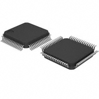
The ADS5421 is available in a small LQFP-64 package.
● COMMUNICATIONS RECEIVERS
● TEST INSTRUMENTATION
● PROFESSIONAL CCD IMAGING
+VS
DV
CLK
ADS5421
Timing Circuitry
CLK
2VPP
14-Bit
Pipelined
ADC
Core
IN
T&H
2VPP
IN
Error
Correction
Logic
3-State
Outputs
D0
•
•
•
D13
CM
(+2.5V)
Reference Ladder
and Driver
Reference and
Mode Select
REFT
VREF SEL1 SEL2
REFB
OE VDRV
Please be aware that an important notice concerning availability, standard warranty, and use in critical applications of
Texas Instruments semiconductor products and disclaimers thereto appears at the end of this data sheet.
All trademarks are the property of their respective owners.
Copyright © 2001-2005 Texas Instruments, Incorporated
PRODUCTION DATA information is current as of publication date.
Products conform to specifications per the terms of Texas Instruments
standard warranty. Production processing does not necessarily include
testing of all parameters.
www.ti.com
�ELECTROSTATIC
DISCHARGE SENSITIVITY
ABSOLUTE MAXIMUM RATINGS(1)
+VSA, +VSD, VDRV ............................................................................... +6V
Analog Input .......................................................... (–0.3V) to (+VS + 0.3V)
Logic Input ............................................................ (–0.3V) to (+VS + 0.3V)
Case Temperature ......................................................................... +100°C
Junction Temperature .................................................................... +150°C
Storage Temperature ..................................................................... +150°C
This integrated circuit can be damaged by ESD. Texas Instruments recommends that all integrated circuits be handled with
appropriate precautions. Failure to observe proper handling
and installation procedures can cause damage.
NOTE: (1) Stresses above these ratings may cause permanent damage.
Exposure to absolute maximum conditions for extended periods may degrade
device reliability. These are stress ratings only, and functional operation of the
device at these or any other conditions beyond those specified is not implied.
ESD damage can range from subtle performance degradation
to complete device failure. Precision integrated circuits may be
more susceptible to damage because very small parametric
changes could cause the device not to meet its published
specifications.
EVALUATION BOARD
PRODUCT
ADS5421EVM
DESCRIPTION
USER’S GUIDE
Populated Evaluation Board
SBAU084
PACKAGE/ORDERING INFORMATION(1)
SPECIFIED
TEMPERATURE
RANGE
PACKAGE
MARKING
PRODUCT
PACKAGE-LEAD
PACKAGE
DESIGNATOR
ADS5421Y
LQFP-64
PM
–40°C to +85°C
ADS5421Y
ADS5421Y/T
Tape and Reel, 250
"
"
"
"
ADS5421Y/R
Tape and Reel, 1500
"
ORDERING
NUMBER
TRANSPORT
MEDIA, QUANTITY
NOTE: (1) For the most current package and ordering information, see the Package Option Addendum at the end of this document, or see the TI website at
www.ti.com.
ELECTRICAL CHARACTERISTICS
TA = specified temperature range, typical at +25°C, +VSA = +VSD = +5V, differential input range = 1.5V to 3.5V each input (4VPP), sampling rate = 40MHz, internal
reference, VDRV = +3V, and –1dBFS, unless otherwise noted.
ADS5421Y
PARAMETER
CONDITIONS
MIN
RESOLUTION
SPECIFIED TEMPERATURE RANGE
ANALOG INPUT
Standard Differential Input Range
Common-Mode Voltage
Optional Input Range
Analog Input Bias Current
Analog Input Bandwidth
Input Capacitance
Ambient Air
Full-Scale = 4VPP
DYNAMIC CHARACTERISTICS
Differential Linearity Error (largest code error)
f = 1MHz
f = 10MHz
No Missing Codes
Integral Nonlinearity Error, f = 1MHz
Spurious-Free Dynamic Range(1)
f = 1MHz
f = 10MHz
f = 30MHz
2-Tone Intermodulation Distortion(3)
f = 14.5MHz and 15.5MHz (–7dB each tone)
Signal-to-Noise Ratio (SNR)
f = 1MHz
f = 10MHz
f = 30MHz
Signal-to-(Noise + Distortion) (SINAD)
f = 1MHz
f = 10MHz
f = 30MHz
Effective Number of Bits(4)
Output Noise
Aperture Delay Time
Aperture Jitter
Over-Voltage Recovery Time
Full-Scale Step Acquisition Time
2
MAX
14 Tested
Bits
°C
3.5
V
V
V
µA
MHz
pF
40M
Samples/sec
Clk Cyc
2.5
3VPP
1
500
9
1M
10
±0.5
±0.5
Tested
±2.5
78
72
72
f = 1MHz
IN and IN tied to CM
UNITS
–40 to +85
1.5
Selectable
CONVERSION CHARACTERISTICS
Sample Rate
Data Latency
TYP
±1.0
LSB
LSB
LSB
88
85
82
dBFS(2)
dBFS
dBFS
–90
dBc
76
75
75
dBFS
dBFS
dBFS
75
74
74
12.2
0.4
3
1
5
5
dB
dB
dBFS
Bits
LSB rms
ns
ps rms
ns
ns
ADS5421
www.ti.com
SBAS237E
�ELECTRICAL CHARACTERISTICS (Cont.)
TA = specified temperature range, typical at +25°C, +VSA = +VSD = +5V, differential input range = 1.5V to 3.5V each input (4VPP), sampling rate = 40MHz, internal
reference, VDRV = +3V, and –1dBFS, unless otherwise noted.
ADS5421Y
PARAMETER
DIGITAL INPUTS
Clock Input
Logic Family (other than clock inputs)
High Level Input Current(5) (VIN = 5V)
Low Level Input Current (VIN = 0V)
High Level Input Voltage
Low Level Input Voltage
Input Capacitance
DIGITAL OUTPUTS(6)
Logic Family
Logic Coding
Low Output Voltage (IOL = 50µA to 0.5mA)
High Output Voltage (IOH = 50µA to 0.5mA)
Low Output Voltage (IOL = 50µA to 1.6mA)
High Output Voltage (IOH = 50µA to 1.6mA)
3-State Enable Time
3-State Disable Time
Output Capacitance
ACCURACY
Zero Error (Referred to –FS)
Zero Error Drift (Referred to –FS)
Gain Error(7)
Gain Error Drift(7)
Power-Supply Rejection of Gain
Internal REF Tolerance (VREFT, VREFB)
External REF Voltage Range
Reference Input Resistance
POWER-SUPPLY REQUIREMENTS
Supply Voltage: +VSA, +VSD
Supply Current: +IS
Output Driver Supply Current (VDRV)
Power Dissipation: VDRV = 5V
VDRV = 3V
Power Down
Thermal Resistance, θJA
LQFP-64
CONDITIONS
MIN
Rising Edge of Convert Clock
+0.5
TYP
MAX
UNITS
+VSD
VPP
100
10
µA
µA
V
V
pF
+3V/+5V Compatible CMOS
+2.0
+1.0
5
+3V/+5V Compatible CMOS
Straight Offset Binary
VDRV = 3V
+0.2
+2.5
VDRV = 5V
+0.2
+2.5
OE = LOW
OE = HIGH
20
2
5
40
10
at +25°C
±0.5
15
±0.2
35
68
±10
2
1.0
±1.0
at +25°C
∆VS = ±5%
Deviation from Ideal
(VREFT – VREFB)
Operating, fIN = 10MHz
Operating, fIN = 10MHz
Operating
1.4
+4.75
+5.0
170
12
900
850
40
48
±1.0
±50
2.025
+5.25
925
V
V
V
V
ns
ns
pF
%FS
ppm/°C
%FS
ppm/°C
dB
mV
V
kΩ
V
mA
mA
mW
mW
mW
°C/W
NOTES: (1) Spurious-Free Dynamic Range refers to the magnitude of the largest harmonic. (2) dBFS means dB relative to Full-Scale. (3) 2-tone intermodulation
distortion is referred to the largest fundamental tone. This number will be 6dB higher if it is referred to the magnitude of the 2-tone fundamental envelope.
(4) Effective Number of Bits (ENOB) is defined by (SINAD – 1.76)/6.02. (5) A 50kΩ pull-down resistor is inserted internally. (6) Recommended maximum
capacitance loading, 15pF. (7) Includes internal reference.
ADS5421
SBAS237E
www.ti.com
3
�PIN CONFIGURATION
REFBY
GND
IN
GND
IN
GND
GND
GND
GND
REFT
CM
REFB
GND
63
GND
64
+VSA
TQFP
+VSA
Top View
62
61
60
59
58
57
56
55
54
53
52
51
50
49
+VSA
1
48 GND
+VSA
2
47 GND
+VSD
3
46 VREF
+VSD
4
45 SEL1
+VSD
5
44 SEL2
+VSD
6
43 GND
GND
7
42 GND
GND
8
CLK
41 BTC
ADS5421Y
9
40 PD
CLK 10
39 OE
GND 11
38 GNDRV
25
26
27
28
29
30
31
32
NC
24
NC
23
B14 (LSB)
22
B13
21
B12
20
B11
19
B10
18
B9
17
B8
33 VDRV
B7
34 VDRV
DV 16
B6
DNC 15
B5
35 VDRV
B4
GNDRV 14
B3
36 GNDRV
B2
37 GNDRV
B1 (MSB)
GND 12
GNDRV 13
PIN DESCRIPTIONS
PIN
1
2
3
4
5
6
7
8
9
10
11
12
13
14
15
16
17
18
19
20
21
22
23
24
25
26
27
28
29
30
31
32
4
I/O
I
I
O
O
O
O
O
O
O
O
O
O
O
O
O
O
DESIGNATOR
+VSA
+VSA
+VSD
+VSD
+VSD
+VSD
GND
GND
CLK
CLK
GND
GND
GNDRV
GNDRV
DNC
DV
B1
B2
B3
B4
B5
B6
B7
B8
B9
B10
B11
B12
B13
B14
NC
NC
DESCRIPTION
Analog Supply Voltage
Analog Supply Voltage
Digital Supply Voltage
Digital Supply Voltage
Digital Supply Voltage
Digital Supply Voltage
Ground
Ground
Clock Input
Complementary Clock Input
Ground
Ground
Ground
Ground
Do Not Connect
Data Valid Pulse: HI = Data Valid
Data Bit 1 (D13) (MSB)
Data Bit 2 (D12)
Data Bit 3 (D11)
Data Bit 4 (D10)
Data Bit 5 (D9)
Data Bit 6 (D8)
Data Bit 7 (D7)
Data Bit 8 (D6)
Data Bit 9 (D5)
Data Bit 10 (D4)
Data Bit 11 (D3)
Data Bit 12 (D2)
Data Bit 13 (D1)
Data Bit 14 (D0) (LSB)
No Internal Connection
No Internal Connection
PIN
33
34
35
36
37
38
39
40
41
42
43
44
45
46
47
48
49
50
51
52
53
54
55
56
57
58
59
60
61
62
63
64
I/O
I
I
I
I
DESIGNATOR
VDRV
VDRV
VDRV
GNDRV
GNDRV
GNDRV
OE
PD
BTC
GND
GND
SEL2
SEL1
VREF
GND
GND
GND
REFB
CM
REFT
GND
GND
GND
GND
IN
GND
IN
GND
REFBY
GND
+VSA
+VSA
DESCRIPTION
Output Driver Supply Voltage
Output Driver Supply Voltage
Output Driver Supply Voltage
Ground
Ground
Ground
Output Enable: HI = High Impedance
Power Down: HI = Power Down; LO = Normal
HI = Binary Two’s Complement
Ground
Ground
Reference Select 2: See Table on Page 5
Reference Select 1: See Table on Page 5
Internal Reference Voltage
Ground
Ground
Ground
Bottom Reference Voltage Bypass
Common-Mode Voltage (Midscale)
Top Reference Voltage Bypass
Ground
Ground
Ground
Ground
Complementary Analog Input
Ground
Analog Input
Ground
Reference Bypass
Ground
Analog Supply Voltage
Analog Supply Voltage
ADS5421
www.ti.com
SBAS237E
�TIMING DIAGRAM
N+9
N+8
N+2
N+1
Analog In
N+4
N+3
N
tD
N+5
tL
tCONV
N + 10
N+7
N+6
tH
Clock
10 Clock Cycles
t2
Data Out
N – 10
N–9
N–8
N–7
N–6
N–5
N–4
N–3
N–2
N–1
Data Invalid
N
t1
Data Valid Output
tDV
SYMBOL
t CONV
tL
tH
tD
t1
t2
tDV
DESCRIPTION
MIN
Convert Clock Period
Clock Pulse LOW
Clock Pulse HIGH
Aperture Delay
Data Hold Time, CL = 0pF
New Data Delay Time, CL = 15pF max
25
11.5
11.5
Data Valid Output, CL = 15pF
3.9
TYP
MAX
UNITS
1µs
t CONV /2
t CONV /2
3
7.2
12.7
ns
ns
ns
ns
ns
ns
4.4
ns
REFERENCE AND FULL-SCALE RANGE SELECT TABLE
DESIRED FULL-SCALE RANGE
SEL1
SEL2
INTERNAL VREF
4VPP
3VPP
GND
GND
GND
+VSA
2V
1.5V
NOTE: For external reference operation, tie VREF to +VSA. The full-scale range will be 2x the reference value. For example, selecting a 2V external reference
will set the full-scale values of 1.5V to 3.5V for both IN and IN inputs.
ADS5421
SBAS237E
www.ti.com
5
�TYPICAL CHARACTERISTICS
TA = 25°C, +VSA = +VSD = +5V, differential input range = 1.5V to 3.5V each input (4VPP), sampling rate = 40MSPS, internal reference, and VDRV = 3V, unless otherwise
noted.
SPECTRAL PERFORMANCE
SPECTRAL PERFORMANCE
0
0
FIN = 1MHz, –1dBFS
FIN = 10MHz, –1dBFS
SFDR = 88.4dBFS
–20
SFDR = 85dBFS
–20
SNR = 74.5dBFS
–40
Amplitude (dB)
Amplitude (dB)
SNR = 76.2dBFS
–60
–80
–100
–40
–60
–80
–100
–120
–120
0
4
8
12
16
20
0
4
8
Frequency (MHz)
SPECTRAL PERFORMANCE
FIN = 15MHz, –1dBFS
FIN = 15MHz, –3dBFS
SFDR = 84.9dBFS
SFDR = 87.9dBFS
–20
SNR = 72.7dBFS
16
20
16
20
SNR = 73.6dBFS
–40
Amplitude (dB)
Amplitude (dB)
20
0
–20
–60
–80
–100
–40
–60
–80
–100
–120
–120
0
4
8
12
16
20
0
4
8
Frequency (MHz)
12
Frequency (MHz)
SPECTRAL PERFORMANCE
2-TONE INTERMODULATION
0
0
FIN = 15MHz, –6dBFS
F1 (–7dBc) = 14.5MHz
SFDR = 85.3dBFS
–20
F2 (–7dBc) = 15.5MHz
–20
SNR = 74.6dBFS
SFDR = –90dB
–40
Amplitude (dB)
Amplitude (dB)
16
SPECTRAL PERFORMANCE
0
–60
–80
–100
–40
–60
–80
–100
–120
–120
0
4
8
12
16
20
0
Frequency (MHz)
6
12
Frequency (MHz)
4
8
12
Frequency (MHz)
ADS5421
www.ti.com
SBAS237E
�TYPICAL CHARACTERISTICS (Cont.)
TA = 25°C, +VSA = +VSD = +5V, differential input range = 1.5V to 3.5V each input (4VPP), sampling rate = 40MSPS, internal reference, and VDRV = 3V, unless otherwise
noted.
DIFFERENTIAL LINEARITY ERROR
0.5
INTEGRAL LINEARITY ERROR
4
FIN = 1MHz
0.4
FIN = 1MHz
3
0.3
2
0.1
ILE (LSB)
DLE (LSB)
0.2
0.0
–0.1
1
0
–1
–0.2
–2
–0.3
–3
–0.4
–0.5
–4
0
2048
4096
6144
8192 10240 12288 14336 16384
0
2048
4096
6144
8192 10240 12288 14336 16384
Code
Code
SFDR AND SNR vs INPUT FREQUENCY
(FCLK = 40MHz)
SFDR AND SNR vs CLOCK FREQUENCY
(FIN = 15MHz)
100
90
SFDR
SFDR
85
SFDR, SNR (dBFS)
SFDR, SNR (dBFS)
90
80
70
SNR
60
50
75
SNR
70
65
40
60
1.0
100
10
10
15
20
25
30
FIN (MHz)
FCLK (MHz)
SFDR AND SNR vs CLOCK FREQUENCY
(FIN = 10MHz)
SWEPT POWER (SFDR)
(FIN = 10MHz)
35
40
–10
0
120
90
SFDR
110
85
dBFS
100
SFDR (dBFS, dBc)
SFDR, SNR (dBFS)
80
80
75
SNR
70
65
90
80
70
60
50
dBc
40
30
20
10
60
0
10
15
20
25
30
35
40
–60
ADS5421
SBAS237E
–50
–40
–30
–20
Input Amplitude (dBFS)
FCLK (MHz)
www.ti.com
7
�TYPICAL CHARACTERISTICS (Cont.)
TA = 25°C, +VSA = +VSD = +5V, differential input range = 1.5V to 3.5V each input (4VPP), sampling rate = 40MSPS, internal reference, and VDRV = 3V, unless otherwise
noted.
SWEPT POWER (SNR)
(FIN = 10MHz)
OUTPUT NOISE HISTOGRAM
(DC Common-Mode Input)
700000
90
dBc
80
600000
500000
60
50
Count
SNR (dBFS, dBc)
70
dBFS
40
30
400000
300000
200000
20
100000
10
0
0
–60
–50
–40
–30
–20
–10
N–3
0
N–2
N–1
Input Amplitude (dBFS)
APPLICATION INFORMATION
THEORY OF OPERATION
The ADS5421 is a high-speed, high-performance, CMOS
ADC build with a fully differential pipeline architecture. Each
stage contains a low-resolution quantizer and digital error
correction logic ensuring good differential linearity. The conversion process is initiated by a rising edge of the external
convert clock. Once the signal is captured by the input trackand-hold amplifier, the bits are sequentially encoded starting
with the Most Significant Bit (MSB). This process results in a
data latency of 10 clock cycles after which the output data is
available as a 14-bit parallel word either coded in a Straight
Offset Binary or Binary Two’s Complement format.
The analog input of the ADS5421 consists of a differential
track-and-hold circuit, as shown in Figure 1. The differential
topology produces a high level of AC performance at high
sampling rates. It also results in a very high usable input
bandwidth—especially important for Intermediate Frequency
(IF) or undersampling applications. Both inputs (IN, IN)
require external biasing up to a common-mode voltage that
is typically at the mid-supply level (+VS/2). This is because
the on-resistance of the CMOS switches is lowest at this
voltage, minimizing the effects of the signal-dependent,
8
N
N+1
N+2
N+3
Code
nonlinearity of RON. For ease of use, the ADS5421 incorporates a selectable voltage reference, a versatile clock input,
and a logic output driver designed to interface to 3V or 5V
logic.
S5
ADS5421
S3
VBIAS
S1
CIN
S2
CIN
IN
T&H
IN
S4
S6
VBIAS
Tracking Phase: S1, S2, S3, S4 closed; S5, S6 open
Hold Phase:
S1, S2, S3, S4 open; S5, S6 closed
FIGURE 1. Simplified Circuit of Input Track-and-Hold Amplifier.
ADS5421
www.ti.com
SBAS237E
�ANALOG INPUTS
TYPES OF APPLICATIONS
The analog input of the ADS5421 can be configured in various
ways and driven with different circuits, depending on the application and the desired level of performance. Offering an extremely high dynamic range at high input frequencies, the
ADS5421 is particularly well suited for communication systems
that digitize wideband signals. Features on the ADS5421, like
the input range selector, or the option of an external reference,
provide the needed flexibility to accommodate a wide range of
applications. In any case, the analog interface/driver requirements should be carefully examined before selecting the appropriate circuit configuration. The circuit definition should include
considerations on the input frequency spectrum and amplitude,
as well as the available power supplies.
DIFFERENTIAL INPUTS
The ADS5421 input structure is designed to accept the applied
signal in differential format. Differential operation of the
ADS5421 requires an input signal that consists of an in-phase
and a 180° out-of-phase component simultaneously applied to
the inputs (IN, IN). Differential signals offer a number of
advantages, which in many applications will be instrumental in
achieving the best harmonic performance of the ADS5421:
• The signal amplitude is half of that required for the singleended operation and is, therefore, less demanding to
achieve while maintaining good linearity performance from
the signal source.
• The reduced signal swing allows for more headroom of
the interface circuitry and, therefore, a wider selection of
the best suitable driver amplifier.
• Even-order harmonics are minimized.
• Improves the noise immunity based on the commonmode input rejection of the converter.
Both inputs are identical in terms of their impedance and
performance with the exception that by applying the signal to
the complementary input (IN) instead of the IN input will invert
the orientation of the input signal relative to the output code.
distortion performance. Here, the SNR number is typically 3dB
down compared to the 4VPP range, while an improvement in
the distortion performance of the driver amplifier may be
realized due to the reduced output power level required.
INPUT BIASING (VCM)
The ADS5421 operates from a single +5V supply, and
requires each of the analog inputs to be externally biased to
a common-mode voltage of typically +2.5V. This allows a
symmetrical signal swing while maintaining sufficient headroom to either supply rail. Communication systems are usually AC-coupled in between signal processing stages, making it convenient to set individual common-mode voltages
and allow optimizing the DC operating point for each stage.
Other applications, such as imaging, process mainly unipolar
or DC-restored signals. In this case, the common-mode
voltage may be shifted such that the full input range of the
converter is utilized.
It should be noted that the CM pin is not internally buffered,
but ties directly to the reference ladder. Therefore, it is
recommended to keep loading of this pin to a minimum
(< 100µA) to avoid an increase in the nonlinearity of the
converter. Additionally, the DC voltage at the CM pin is not
precisely +2.5V, but is subject to the tolerance of the top and
bottom references, as well as the resistor ladder. Furthermore, the common-mode voltage typically declines with an
increase in sampling frequency. This, however, does not
affect the performance.
INPUT IMPEDANCE
The input of the ADS5421 is capacitive, and the driving source
needs to provide the slew current to charge or discharge the
input sampling capacitor while the track-and-hold amplifier is
in track mode (see Figure 1). This effectively results in a
dynamic input impedance that is a function of the sampling
frequency. Figure 2 depicts the differential input impedance of
the ADS5421 as a function of the input frequency.
INPUT FULL-SCALE RANGE VERSUS PERFORMANCE
100
ZIN (kΩ)
Employing dual-supply amplifiers and AC-coupling will usually
yield the best results. DC-coupling and/or single-supply amplifiers impose additional design constraints due to their headroom requirements, especially when selecting the
4VPP input range. The full-scale input range of the ADS5421
is defined either by the settings of the reference select pins
(SEL1, SEL2) or by an external reference voltage
(see Table I). By choosing between the different signal input
ranges, trade-offs can be made between noise and distortion
performance. For maximizing the SNR—important for timedomain applications—the 4VPP range may be selected. This
range may also be used with low-level (–6dBFS to –40dBFS)
but high-frequency inputs (multi-tone). The 3VPP range may be
considered for achieving a combination of both low-noise and
1000
10
1
0.1
0.01
0.1
1
10
100
1000
fIN (MHz)
FIGURE 2. Differential Input Impedance vs Input Frequency.
ADS5421
SBAS237E
www.ti.com
9
�For applications that use op amps to drive the ADC, it is
recommended that a series resistor be added between the
amplifier output and the converter inputs. This will isolate the
capacitive input of the converter from the driving source and
avoid gain peaking, or instability; furthermore, it will create a
1st-order, low-pass filter in conjunction with the specified
input capacitance of the ADS5421. Its cutoff frequency can
be adjusted further by adding an external shunt capacitor
from each signal input to ground. The optimum values of this
RC network, however, depend on a variety of factors, including the ADS5421 sampling rate, the selected op amp, the
interface configuration, and the particular application (time
domain versus frequency domain). Generally, increasing the
size of the series resistor and/or capacitor will improve the
SNR, however, depending on the signal source, large resistor values may be detrimental to the harmonic distortion
performance. In any case, the use of the RC network is
optional but optimizing the values to adapt to the specific
application is encouraged.
ANALOG INPUT DRIVER CONFIGURATIONS
The following section provides some principal circuit suggestions on how to interface the analog input signal to the
ADS5421. Applications that have a requirement for DCcoupling a new differential amplifier, such as the THS4502,
can be used to drive the ADS5421, as shown in Figure 3. The
THS4502 amplifier allows a single-ended to differential conversion to be performed easily, which reduces component
cost. In addition, the VCM pin on the THS4502 can be directly
tied to the common-mode pin (CM) of the ADS5421 in order
to set up the necessary bias voltage for the converter inputs.
As shown in Figure 3, the THS4502 is configured for unity
gain. If required, higher gain can easily be configured, and a
low-pass filter can be created by adding small capacitors
(e.g., 10pF) in parallel to the feedback resistors. Due to the
THS4502 driving a capacitive load, small series resistors in
the output ensure stable operation. Further details of this and
other functions of the THS4502 may be found in its product
datasheet located at the Texas Instruments web site
(www.ti.com). In general, differential amplifiers provide for a
high-performance driver solution for baseband applications,
and different differential amplifier models can be selected
depending on the system requirements.
TRANSFORMER-COUPLED INTERFACE CIRCUITS
If the application allows for AC-coupling but requires a signal
conversion from a single-ended source to drive the ADS5421
differentially, using a transformer offers a number of advantages. As a passive component, it does not add to the total
noise, and by using a step-up transformer, further signal
amplification can be realized. As a result, the signal swing of
the amplifier driving the transformer can be reduced, leading
to an increased headroom for the amplifier and improved
distortion performance.
A transformer interface solution is given in Figure 4. The
input signal is assumed to be an IF and bandpass filtered
prior to the IF amplifier. Dedicated IF amplifiers are commonly fixed-gain blocks and feature a very high bandwidth,
low-noise figure, and a high intercept point, but at the
expense of high quiescent currents, which are often around
100mA. The IF amplifier may be AC-coupled, or directly
connected to the primary side of the transformer. A variety of
miniature RF transformers are readily available from different
manufacturers, (e.g., Mini-Circuits, Coilcraft, or Trak). For
selection, it is important to carefully examine the application
requirements and determine the correct model, the desired
impedance ratio, and frequency characteristics. Furthermore,
the appropriate model must support the targeted distortion
level and should not exhibit any core saturation at full-scale
voltage levels. The transformer center tap can be directly tied
to the CM pin of the converter because it does not appreciably
load the ADC reference (see Figure 4). The value of termination resistor RT must be chosen to satisfy the termination
requirements of the source impedance (RS). It can be calculated using the equation RT = n2 • RS to ensure proper
impedance matching.
+5V
10pF(1)
+5V
392Ω
RS
392Ω
25Ω
IN
56.2Ω
VCM
THS4502
25Ω
ADS5421
22pF
IN
0.1µF
392Ω
412Ω
CM
10pF(1)
–5V
NOTES: Supply bypassing not shown. (1) Optional.
FIGURE 3. Using the THS4502 Differential Amplifier (Gain = 1) to Drive the ADS5421 in a DC-Coupled Configuration.
10
ADS5421
www.ti.com
SBAS237E
�+5V
VIN (IF)
Optional
Bandpass
Filter
RS
IF
Amplifier
XFR
1:n
RIN
IN
RT
RIN
CIN
ADS5421
IN
CM
NOTE: Supply bypassing not shown.
+
0.1µF
2.2µF
FIGURE 4. Driving the ADS5421 with a Low-Distortion IF Amplifier and a Transformer Suited for IF Sampling Applications.
TRANSFORMER-COUPLED, SINGLE-ENDED-TODIFFERENTIAL CONFIGURATION
For applications in which the input frequency is limited to
approximately 10MHz (e.g., baseband), a high-speed operational amplifier may be used. The OPA847 is configured for the
noninverting mode; this amplifies the single-ended input signal
and drives the primary of a RF transformer (see Figure 5). To
maintain the very low distortion performance of the OPA847, it
may be advantageous to set the full-scale input range of the
ADS5421 to 3VPP.
The circuit also shows the use of an additional RC low-pass
filter placed in series with each converter input. This optional
filter can be used to set a defined corner frequency and
attenuate some of the wideband noise. The actual component values would need to be tuned for individual application
requirements. As a guideline, resistor values are typically in
the range of 10Ω to 50Ω, and capacitors in the range of 10pF
to 100pF. In any case, the RIN and CIN values should have
a low tolerance. This will ensure that the ADS5421 sees
closely matched source impedances.
+5V –5V
+5V
RG
RS
VIN
OPA847
0.1µF
RIN
1:n
IN
RT
R1
RIN
CIN
ADS5421
IN
VCM ≈ +2.5V
CM
R2
+
2.2µF
0.1µF
FIGURE 5. Converting a Single-Ended Input Signal into a Differential Signal Using a RF Transformer.
ADS5421
SBAS237E
www.ti.com
11
�AC-COUPLED, DIFFERENTIAL INTERFACE WITH
GAIN
sets a pole at approximately 85MHz and rolls off some of the
wideband noise resulting in a reduction of the noise floor.
The interface circuit example presented in Figure 6 employs
two OPA687s, (decompensated voltage-feedback op amps),
optimized for gains of 12V/V or higher. Implementing a new
compensation technique allows the OPA847s to operate with
a reduced signal gain of 8.5V/V, while maintaining the high
loop gain and the associated excellent distortion performance offered by the decompensated architecture. For a
detailed discussion on this circuit and the compensation
scheme, refer to the OPA847 data sheet (SBOS251) located
at www.ti.com. Input transformer, T1, converts the singleended input signal to a differential signal required at the
inverting inputs of the amplifier, which are tuned to provide a
50Ω impedance match to an assumed 50Ω source. To
achieve the 50Ω input match at the primary of the 1:2
transformer, the secondary must see a 200Ω load impedance. Both amplifiers are configured for the inverting mode
resulting in close gain and phase matching of the differential
signal. This technique, along with a highly symmetrical layout, is instrumental in achieving a substantial reduction of the
2nd-harmonic, while retaining excellent 3rd-order performance. A common-mode voltage, VCM, is applied to the
noninverting inputs of the OPA847. Additional series 20Ω
resistors isolate the output of the op amps from the capacitive load presented by the 40pF capacitors and the input
capacitance of the ADS5421. This 20Ω/47pF combination
For the measured 2-tone, 3rd-order distortion for the amplifier portion of the circuit of Figure 6, see Figure 7. The curve
is for a total 2-tone envelope of 4VPP, requiring two tones,
each 2VPP across the OPA847 outputs. The basic measurement dynamic range for the two close-in spurious tones is
approximately 85dBc. The 4VPP test does not show measurable 3rd-order spurious until 25MHz.
3rd-Order Spurious (dBc)
–60
–65
4VPP
–70
–75
–80
–85
0
5
10
15
20
25
30
35
40
45
50
Center Frequency (MHz)
FIGURE 7. Measured 2-Tone, 3rd-Order Distortion for a
Differential ADC Driver.
+5V
VCM
100Ω
20Ω
OPA847
–5V
+5V
1.7pF
T1
50Ω Source
1:2
39pF
850Ω
IN
< 6dB
Noise
Figure
39pF
ADS5421
47pF
850Ω
IN
CM
1.7pF
100Ω
VCM
+5V
20Ω
0.1µF
OPA847
VCM
–5V
FIGURE 6. High Dynamic Range Interface Circuit with the OPA847 Set for a Gain of +8.5V/V.
12
ADS5421
www.ti.com
SBAS237E
�REFERENCE
REFERENCE OPERATION
Integrated into the ADS5421 is a bandgap reference circuit,
including logic that provides a +1.5V or +2V reference
output by selecting the corresponding pin-strap configuration. Table I lists an overview of the possible reference
options and pin configurations.
Figure 8 shows the basic model of the internal reference
circuit. The functional blocks are a 1V bandgap voltage
reference, a selectable gain amplifier, the drivers for the top
and bottom reference (REFT, REFB), and the resistive reference ladder. The ladder resistance measures approximately
1kΩ between the REFT and REFB pins. The ladder is split
into two equal segments establishing a common-mode voltage at the ladder midpoint, labeled CM. The ADS5421
requires solid bypassing for all reference pins to keep the
effects of clock feedthrough to a minimum and to achieve the
specified level of performance. Figure 8 shows the recommended decoupling scheme. All 0.1µF capacitors must be
located as close to the pins as possible. In addition, pins
REFT, CM, and REFB must be decoupled with tantalum
surface-mount capacitors (2.2µF or 4.7µF).
When operating the ADS5421 with the internal reference, the
effective full-scale input span for each of the inputs, IN and
IN, is determined by the voltage at the VREF pin, given to:
(1)
Input Span (differential, each input) = VREF = (REFT – REFB) in VPP
DESIRED FULL-SCALE
RANGE (FSR)
(DIFFERENTIAL)
The top and bottom reference outputs can be used to provide
up to 1mA of current (sink or source) to external circuits.
Degradation of the differential linearity (DNL) and, consequently, the dynamic performance, of the ADS5421 may
occur if this limit is exceeded.
USING EXTERNAL REFERENCES
For even more design flexibility, the ADS5421 can be operated with external references. The utilization of an external
reference voltage may be considered for applications requiring higher accuracy, improved temperature stability, or a
continuous adjustment of the converter full-scale range.
Especially in multichannel applications, the use of a common
external reference offers the benefit of improving the gain
matching between converters. Selection between internal or
external reference operation is controlled through the VREF
pin. The internal reference will become disabled if the voltage
applied to the VREF pin exceeds +3.5VDC. Once selected, the
ADS5421 requires two reference voltages: a top reference
voltage applied to the REFT pin and a bottom reference
voltage applied to the REFB pin (see Table I). The full-scale
range is determined by FSR = 2 x (VREFT – VREFB). It is
recommended to maintain the common-mode voltage at
+2.5V. As illustrated in Figure 9, a micropower reference
(REF1004) and a dual, single-supply amplifier (OPA2234)
can be used to generate a precision external reference. Note
that the function of the range select pins, SEL1 and SEL2,
are disabled while the converter is operating in external
reference mode.
CONNECT
SEL1 (PIN 45) TO:
CONNECT
SEL2 (PIN 44) TO:
4VPP (+16dBm)
GND
GND
+2.0V
+3.5V
+1.5V
3VPP (+13dBm)
GND
+VSA
+1.5V
+3.25V
+1.75V
—
—
> +3.5V
+3.2V to +3.5V
+1.5V to +1.8V
External Reference
VOLTAGE AT VREF
(PIN 46)
VOLTAGE AT REFT
(PIN 52)
VOLTAGE AT REFB
(PIN 50)
TABLE I. Reference Pin Configurations and Corresponding Voltages on the Reference Pins.
SEL1 SEL2
45
REFBY
61
0.1µF
44
Range Select
and
Gain Amplifier
Top
Reference
Driver
REFT
52
0.1µF
+
2.2µF
500Ω
CM
+1VDC
Bandgap
Reference
51
0.1µF
+
2.2µF
500Ω
Bottom
Reference
Driver
ADS5421
REFB
50
0.1µF
+
2.2µF
46
VREF
0.1µF
FIGURE 8. Internal Reference Circuit of the ADS5421 and Recommended Bypass Scheme.
ADS5421
SBAS237E
www.ti.com
13
�+5V
+5V
1/2
OPA2234
4.7kΩ
REFT
+
R3
+
0.1µF
ADS5421
R4
R1
REF1004
+2.5V
2.2µF
10µF
1/2
OPA2234
R2
REFB
+
0.1µF
2.2µF
0.1µF
FIGURE 9. Example for an External Reference Circuit Using a Dual, Single-Supply Op Amp.
DIGITAL INPUTS AND OUTPUTS
CLOCK INPUT
CLK
Unlike most ADCs, the ADS5421 contains internal clock
conditioning circuitry. This enables the converter to adapt to
a variety of application requirements and different clock
sources. With no input signal connected to either clock pin,
the threshold level is set to approximately +1.6V by the onchip resistive voltage divider, as shown in Figure 10. The
parallel combination of R1 || R2 and R3 || R4 sets the input
impedance of the clock inputs (CLK, CLK) to approximately
2.7kΩ single-ended, or 5.5kΩ differentially. The associated
ground referenced input capacitance is approximately 5pF
for each input. If a logic voltage other than the nominal +1.6V
is desired, the clock inputs can be externally driven to
establish an alternate threshold voltage.
+5V
R1
8.5kΩ
ADS5421
R3
8.5kΩ
CLK
CLK
R2
4kΩ
R4
4kΩ
FIGURE 10. The Differential Clock Inputs are Internally Biased.
The ADS5421 can be interfaced to standard TTL or CMOS
logic and accepts 3V or 5V compliant logic levels. In this
case, the clock signal should be applied to the CLK input,
whereas the complementary clock input (CLK) should be
bypassed to ground by a low-inductance ceramic chip capacitor, as shown in Figure 11. Depending on the quality of
the signal, inserting a series, damping resistor can be beneficial to reduce ringing. When digitizing at high sampling rates
the clock should have a 50% duty cycle (tH = tL) to maintain
good distortion performance.
TTL/CMOS
Clock Source
(3V/5V)
ADS5421
CLK
47nF
FIGURE 11. Single-Ended TTL/CMOS Clock Source.
Applying a single-ended clock signal will provide satisfactory
results in many applications. However, unbalanced high-speed
logic signals can introduce a high amount of disturbances,
such as ringing or ground bouncing. In addition, a high
amplitude can cause the clock signal to have unsymmetrical
rise-and-fall times, potentially affecting the converter distortion
performance. Proper termination practice and a clean PC
board layout will help to keep those effects to a minimum.
To take full advantage of the excellent distortion performance
of the ADS5421, it is recommended to drive the clock inputs
differentially. A differential clock improves the digital
feedthrough immunity and minimizes the effect of modulation
between the signal and the clock. Figure 12 illustrates a
simple method of converting a square wave clock from
single-ended to differential using an RF transformer. Small
surface-mount transformers are readily available from several manufacturers (e.g., model ADT1-1 by Mini-Circuits). A
capacitor in series with the primary side may be inserted to
block any DC voltage present in the signal. The secondary
side connects directly to the two clock inputs of the converter
because the clock inputs are self-biased.
Square Wave
or Sine Wave
Clock Source
RS
XFR
1:1
0.1µF
RT
CLK
ADS5421
CLK
FIGURE 12. Connecting a Ground-Referenced Clock Source
to the ADS5421 Using an RF Transformer.
14
ADS5421
www.ti.com
SBAS237E
�MINIMUM SAMPLING RATE
The clock inputs of the ADS5421 can be connected in a
number of ways. However, the best performance is obtained
when the clock input pins are driven differentially. Operating in
this mode, the clock inputs accommodate signal swings ranging from 2.5VPP down to 0.5VPP differentially. This allows direct
interfacing of clock sources such as voltage-controlled crystal
oscillators (VCXO) to the ADS5421. The advantage here is the
elimination of external logic, usually necessary to convert the
clock signal into a suitable logic (TTL or CMOS) signal that
otherwise would create an additional source of jitter. In any
case, a very low-jitter clock is fundamental to preserving the
excellent AC performance of the ADS5421. The converter
itself is specified for a low jitter, characterizing the outstanding
capability of the internal clock and track-and-hold circuitry.
Generally, as the input frequency increases, the clock jitter
becomes more dominant for maintaining a good signal-tonoise ratio. This is particularly critical in IF sampling applications where the sampling frequency is lower than input frequency (undersampling). The following equation can be used
to calculate the achievable SNR for a given input frequency
and clock jitter (tJA in ps rms):
SNR = 20 log10
1
π
2
f
( INt JA )
The pipeline architecture of the ADS5421 uses a switchedcapacitor technique in its internal track-and-hold stages. With
each clock cycle, charges representing the captured signal
level are moved within the ADC pipeline core. The high
sampling speed necessitates the use of very small capacitor
values. In order to hold the droop errors low, the capacitors
require a minimum refresh rate. To maintain accuracy of the
acquired sample charge, the sampling clock on the ADS5421
must not drop below the specified minimum of 1MHz.
DATA OUTPUT FORMAT (BTC)
The ADS5421 makes two data output formats available,
either the Straight Offset Binary (SOB) code or the Binary
Two’s Complement (BTC) code. The selection of the output
coding is controlled through the BTC pin. Applying a logic
HIGH will enable the BTC coding, whereas a logic LOW will
enable the SOB code. The BTC output format is widely used
to interface to microprocessors, for example. The two code
structures are identical with the exception that the MSB is
inverted for the BTC format, as shown in Table II.
(2)
If the input signal exceeds the full-scale range, the data
outputs will exhibit the respective full-scale code depending
on the selected coding format.
Depending on the nature of the clock source output impedance, impedance matching might become necessary. For
this, a termination resistor, RT, can be installed (see Figure
12). To calculate the correct value for this resistor, consider
the impedance ratio of the selected transformer and the
differential clock input impedance of the ADS5421, which is
approximately 5.5kΩ.
Shown in Figure 13 is one preferred method for clocking the
ADS5421. Here, the single-ended clock source can be either
a square wave or a sine wave. Using the high-speed differential translator SN65LVDS100 from Texas Instruments, a
low-jitter clock can be generated to drive the clock inputs of
the ADS5421 differentially.
DIFFERENTIAL
INPUT
STRAIGHT OFFSET
BINARY (SOB)
BINARY TWO’S
COMPLEMENT
(BTC)
+FS – 1LSB
(IN = +3.5V, IN = +1.5V)
11 1111 1111 1111
01 1111 1111 1111
+1/2 FS
11 0000 0000 0000
01 0000 0000 0000
Bipolar Zero
(IN = IN = VCM)
10 0000 0000 0000
00 0000 0000 0000
–1/2 FS
01 0000 0000 0000
11 0000 0000 0000
–FS
(IN = +1.5V, IN = +3.5V)
00 0000 0000 0000
10 0000 0000 0000
TABLE II. Coding Table for Differential Input Configuration
and 4VPP Full-Scale Input Range.
+5V
0.01µF
Square Wave
Or Sine Wave
Clock Input
SN65LVDS100
0.01µF
A
RT(1)
100Ω
0.01µF
Y
CLK
B
0.01µF
Z
VBB
ADS5421
CLK
50Ω
50Ω
0.01µF
NOTE: (1) Additional termination resistor RT may be necessary depending on the source requirements
FIGURE 13. Differential Clock Driver Using an LVDS Translator.
ADS5421
SBAS237E
www.ti.com
15
�OUTPUT ENABLE (OE )
POWER DISSIPATION
The digital outputs of the ADS5421 can be set to high
impedance (tri-state), exercising the output enable pin (OE).
For normal operation, this pin must be at a logic LOW
potential, whereas a logic HIGH voltage disables the outputs.
Even though this function affects the output driver stage, the
threshold voltages for the OE pin do not depend on the
output driver supply (VDRV), but are fixed (see the Electrical
Characteristics Table and the Digital Inputs Sections). Operating the OE function dynamically (e.g., high-speed multiplexing) should be avoided as it will corrupt the conversion
process.
A majority of the ADS5421 total power consumption is used
for biasing, therefore; it is independent of the applied clock
frequency. Figure 14 shows the typical variation in power
consumption versus the clock speed. The current on the
VDRV supply is directly related to the capacitive loading of
the data output pins and care must be taken to minimize
such loading.
45
FIN = 10MHz
40
Sample Rate (MSPS)
POWER-DOWN (PD)
A power-down pin is provided; when taken HIGH, this pin
shuts down portions within the ADS5421 and reduces the
power dissipation to less than 40mW. The remaining active
blocks include the internal reference, ensuring a fast reactivation time. During power-down, data in the converter pipeline will be lost and new valid data will be subject to the
specified pipeline delay. If the PD pin is not used, it should
be tied to ground or a logic LOW level.
35
30
25
20
15
700
720
740
760
780
800
820
840
880
Power Dissipation (mW)
OUTPUT LOADING
It is recommended to keep the capacitive loading on the data
output lines as low as possible, preferably below 15pF.
Higher capacitive loading will cause larger dynamic currents
as the digital outputs are changing. For example, with a
typical output slew rate of 0.8V/ns and a total capacitive
loading of 10pF (including 4pF output capacitance, 5pF input
capacitance of external logic buffer, and 1pF PC board
parasitics), a bit transition can cause a dynamic current of
(10pF • 0.8V/1ns = 8mA). These high current surges can
feed back to the analog portion of the ADS5421 and adversely affect the performance. If necessary, external buffers
or latches close to the converter’s output pins can be used to
minimize the capacitive loading. They also provide the added
benefit of isolating the ADS5421 from any digital activities on
the bus coupling back high-frequency noise.
POWER SUPPLIES
When defining the power supplies for the ADS5421, it is
highly recommended to consider linear supplies instead of
switching types. Even with good filtering, switching supplies
can radiate noise that could interfere with any highfrequency input signal and cause unwanted modulation products. At its full conversion rate of 40MHz, the ADS5421
typically requires 170mA of supply current on the +5V supplies. Note that this supply voltage should stay within a 5%
tolerance.
16
FIGURE 14. Power Dissipation vs Clock Frequency.
DIGITAL OUTPUT DRIVER SUPPLY (VDRV)
A dedicated supply pin, VDRV, provides power to the logic
output drivers of the ADS5421 and can be operated with a
supply voltage in the range of +3.0V to +5.0V. This can
simplify interfacing to various logic families, in particular lowvoltage CMOS. It is recommended to operate the ADS5421
with a +3.3V supply voltage on VDRV. This will lower the
power dissipation in the output stages due to the lower output
swing and reduce current glitches on the supply line that may
affect the AC performance of the converter. The analog
supply (+VSA) and digital supply (+VSD) may be tied together,
with a ferrite bead or inductor between the supply pins. Each
of the these supply pins must be bypassed separately with at
least one 0.1µF ceramic chip capacitor, forming a pi-filter
(see Figure 15). The recommended operation for the ADS5421
is +5V for the +VS pins and +3.3V on the output driver pin
(VDRV).
The configuration of the supplies requires that a specific
power-up sequence be followed for the ADS5421. Analog
voltage must be applied to the analog supply pin (+VSA)
before applying a voltage to the driver supply (VDRV) or
before bringing both the digital supply (+VSD) and VDRV up
simultaneously. Powering up +VSD and VDRV prior to +VSA
will cause a large current on +VSA and result in the ADS5421
not functioning properly.
ADS5421
www.ti.com
SBAS237E
�VIN
50Ω
ADT2-1
4.7µF
+
+VA
(5V)
0.1µF
0.1µF
22Ω
22Ω
4.7µF
+
4.7µF
+
0.1µF
0.1µF
22pF
56
55
54
53
52
51
50
49
GND
GND
IN
GND
IN
GND
GND
GND
GND
REFT
CM
REFB
GND
+VSA
57
GND
48
GND
47
+VSD
VREF
46
+VSD
SEL1
45
5
+VSD
SEL2
44
6
+VSD
GND
43
7
GND
GND
42
8
GND
BTC
41
9
CLK
PD
40
10
CLK
OE
39
11
GND
GNDRV
38
12
GND
GNDRV
37
13
GNDRV
GNDRV
36
14
GNDRV
VDRV
35
15
DNC
VDRV
34
16
DV
VDRV
33
B8
B9
B10
B11
B12
B13
B14
NC
NC
ADS5421
B7
50Ω
4
58
B6
0.1µF ADT2-1
3
59
B5
RS
CLKIN
+VSA
60
B4
0.1µF
10µF
2
61
B3
+VD
(5V)
+VSA
62
B2
0.01µF
1
63
B1
0.1µF
64
+VSA
10µF
+
0.1µF
REFBY
0.1µF
17
18
19
20
21
22
23
24
25
26
27
28
29
30
31
32
0.1µF
0.01µF
NC
NC
D13
D12
D11
D9
D10
D8
D7
D6
D5
D4
D3
D2
D1
DV
DO
0.1µF
10µF
+
0.1µF
+VDR
(3.3V)
FIGURE 15. Basic Application Circuit of the ADS5421 Includes Recommended Supply and Reference Bypassing.
ADS5421
SBAS237E
www.ti.com
17
�LAYOUT AND DECOUPLING
CONSIDERATIONS
Proper grounding and bypassing, short lead length, and the
use of ground planes are particularly important for highfrequency designs. Achieving optimum performance with a
fast sampling converter like the ADS5421 requires careful
attention to the PC board layout to minimize the effect of
board parasitics and optimize component placement. A multilayer board usually ensures best results and allows convenient component placement.
The ADS5421 must be treated as an analog component and
the +VSA pins connected to a clean analog supply. This
ensures the most consistent results, because digital supplies
often carry a high level of switching noise that could couple
into the converter and degrade the performance. As mentioned previously, the driver supply pins (VDRV) must also
be connected to a low-noise supply. Supplies of adjacent
digital circuits can carry substantial current transients. The
supply voltage must be thoroughly filtered before connecting
to the VDRV supply of the converter. All ground connections
on the ADS5421 are internally bonded to the metal flag
(bottom of package) that forms a large ground plane. All
ground pins must directly connect to an analog ground plane
that covers the PC board area under the converter.
Due to its high sampling frequency, the ADS5421 generates
high-frequency current transients and noise (clock
feedthrough) that are fed back into the supply and reference
lines. If not sufficiently bypassed, this adds noise to the
conversion process. See Figure 15 for the recommended
supply decoupling scheme for the ADS5421. All +VS pins
should be bypassed with a combination of 10nF, 0.1µF
ceramic chip capacitors (0805, low ESR) and a 10µF tantalum tank capacitor. A similar approach may be used on the
driver supply pins, VDRV. In order to minimize the lead and
trace inductance, the capacitors must be located as close to
18
the supply pins as possible. They are best placed directly
under the package where double-sided component mounting
is allowed. In addition, larger bipolar decoupling capacitors
(2.2µF to 10µF), effective at lower frequencies, must also be
used on the main supply pins. They can be placed on the PC
board in proximity (< 0.5") of the ADC.
If the analog inputs to the ADS5421 are driven differentially,
it is especially important to optimize towards a highly symmetrical layout. Small trace length differences can create
phase shifts compromising a good distortion performance.
For this reason, the use of two single op amps rather than
one dual amplifier enables a more symmetrical layout and a
better match of parasitic capacitances. The pin orientation of
the ADS5421 package follows a flow-through design with the
analog inputs located on one side of the package whereas
the digital outputs are located on the opposite side of the
quad-flat package. This provides a good physical isolation
between the analog and digital connections. While designing
the layout, it is important to keep the analog signal traces
separated from any digital lines to prevent noise coupling
onto the analog portion.
Try to match trace length for the differential clock signal (if
used) to avoid mismatches in propagation delays. Singleended clock lines must be short and should not cross any
other signal traces.
Short circuit traces on the digital outputs will minimize capacitive loading. Trace length must be kept short to the receiving
gate (< 2") with only one CMOS gate connected to one digital
output. If possible, the digital data outputs must be buffered
(with the TI SN74AVC16244, for example). Dynamic performance can also be improved with the insertion of series
resistors at each data output line. This sets a defined time
constant and reduces the slew rate that would otherwise flow
due to the fast edge rate. The resistor value may be chosen
to result in a time constant of 15% to 25% of the used data
rate.
ADS5421
www.ti.com
SBAS237E
�Revision History
DATE
REVISION
PAGE
SECTION
—
—
1
Features
2
Electrical Characteristics
Changed Optional Input Ranges to Optional Input Range and deleted 2Vp-p,
same line under TYP.
3
Electrical Characteristics
Changed External REF Voltage Range from 9.9V to 1.4V (minimum). Added
(VREFT – VREFB) to ACCURACY section under CONDITIONS column.
5
Reference and Full-Scale
Range Select Table
9
Input Full-Scale Range
Versus Performance
11
Transformer-Coupled,
Single-Ended-toDifferential Configuration
Deleted part of the last sentence in the first paragraph.
AC-Coupled, Differential
Interface with Gain
Text change in last paragraph.
Front Page Diagram
6/21/05
E
DESCRIPTION
12
Figure 7
13
Reference Operation
Using External References
Table I
16
Data Output Format (BTC)
Changed all Vp-p to subscript (VPP).
Changed PREMIUM to ON-BOARD. Deleted LOW POWER: 850mW.
Changed 1Vp-p to 2VPP.
Deleted 2Vp-p row.
Deleted last sentence.
Deleted 2Vp-p curve.
Deleted +1V and the word complete in first paragraph.
Inserted text.
Deleted 2Vp-p row. Changed voltages at REFT and REFB columns in
External Reference row.
Changed and deleted text in second paragraph.
NOTE: Page numbers for previous revisions may differ from page numbers in the current version.
ADS5421
SBAS237E
www.ti.com
19
�PACKAGE OPTION ADDENDUM
www.ti.com
10-Dec-2020
PACKAGING INFORMATION
Orderable Device
Status
(1)
Package Type Package Pins Package
Drawing
Qty
Eco Plan
(2)
Lead finish/
Ball material
MSL Peak Temp
Op Temp (°C)
Device Marking
(3)
(4/5)
(6)
ADS5421Y/T
ACTIVE
LQFP
PM
64
250
RoHS & Green
NIPDAU
Level-3-260C-168 HR
-40 to 85
ADS5421Y
(1)
The marketing status values are defined as follows:
ACTIVE: Product device recommended for new designs.
LIFEBUY: TI has announced that the device will be discontinued, and a lifetime-buy period is in effect.
NRND: Not recommended for new designs. Device is in production to support existing customers, but TI does not recommend using this part in a new design.
PREVIEW: Device has been announced but is not in production. Samples may or may not be available.
OBSOLETE: TI has discontinued the production of the device.
(2)
RoHS: TI defines "RoHS" to mean semiconductor products that are compliant with the current EU RoHS requirements for all 10 RoHS substances, including the requirement that RoHS substance
do not exceed 0.1% by weight in homogeneous materials. Where designed to be soldered at high temperatures, "RoHS" products are suitable for use in specified lead-free processes. TI may
reference these types of products as "Pb-Free".
RoHS Exempt: TI defines "RoHS Exempt" to mean products that contain lead but are compliant with EU RoHS pursuant to a specific EU RoHS exemption.
Green: TI defines "Green" to mean the content of Chlorine (Cl) and Bromine (Br) based flame retardants meet JS709B low halogen requirements of