User's Guide
SLAU449A – August 2012 – Revised September 2013
ADS61JBxx EVM User’s Guide
This document is intended to serve as a user’s guide for the ADS61JBxx EVM (EVM). The ADS61JB23
EVM provides a platform for evaluating the ADS61JB23, which is a single channel, 12-bit ADC operating
at sampling rates of up to 80 Msps, with the digital data output on a JESD204 8b10b-coded serial link at
data rates of up to 1.6 Gbps. The ADS61JB46 EVM supports the 14-bit, 160 Msps ADS61JB46.
This EVM is ideally suited for mating with the TSW1200 or TSW1400 Capture Cards for performing a data
capture into a capture buffer, uploading the sample data to a PC, performing an FFT, and reporting on
SNR, SFDR, and other performance metrics. Since the TSW1200 does not have native support for
JESD204 serial links, the ADS61JBxx EVM has an FPGA to deserialize the sample data and reformat it to
an LVDS DDR parallel data format that the Capture Card can accept.
1
2
3
Contents
Overview ..................................................................................................................... 2
Software Control ............................................................................................................ 9
Basic Test Procedure ..................................................................................................... 11
List of Figures
1
Simplified EVM Block Diagram ............................................................................................
2
2
Simplified EVM Power Supply .............................................................................................
3
3
EVM Jumpers and Switches...............................................................................................
4
4
EVM Solder Options ........................................................................................................
6
5
CML Termination Options ..................................................................................................
8
6
Control Options ..............................................................................................................
9
7
Test Setup Block Diagram
...............................................................................................
TSW1200 FFT Result .....................................................................................................
11
8
13
List of Tables
1
2
......................................................................................................
Surface Mount Jumpers ....................................................................................................
Square Post Jumpers
SLAU449A – August 2012 – Revised September 2013
Submit Documentation Feedback
Copyright © 2012–2013, Texas Instruments Incorporated
ADS61JBxx EVM User’s Guide
7
8
1
�Overview
www.ti.com
1
Overview
1.1
EVM Block Diagram
Figure 1 shows a simplified block diagram of the default configuration of the EVM. The analog input is
supplied to the EVM through a single-ended SMA connection, then transformer coupled to turn the single
ended signal into a balanced differential signal, and then input to the ADS61JBxx. A dual transformer input
circuit is used for better phase and amplitude balance of the input signal than would typically be produced
by a single transformer input circuit.
USB
J6
SPI Port
Analog Input
3.125
Gbps
ADS61JBxx
J19
Sync
FPGA
LVDS DDR
CLK, DATA
Clock
Reference Clock
5V
J10
Power
Supply
Circuits
Figure 1. Simplified EVM Block Diagram
The clock input is supplied by way of a single-ended signal to an SMA connector and transformer coupled
to produce a differential clock signal for the ADS61JBxx.
Power to the EVM is supplied by a single 5-V connection by way of banana jacks. All necessary voltages
for the ADS61JBxx are derived from the 5-V input connection.
2
ADS61JBxx EVM User’s Guide
SLAU449A – August 2012 – Revised September 2013
Submit Documentation Feedback
Copyright © 2012–2013, Texas Instruments Incorporated
�Overview
www.ti.com
1.2
EVM Power Supply
Figure 2 shows the power supply options available on the ADS61JBxx EVM. Jumpers are used to choose
the power supply options. The default jumper position is indicated by the darker portion of the jumper that
represents the presence of the jumper.
There are two power supply options for getting the 5-V power to the EVM. The 5-V power may be input
directly to the banana jack (J10). Alternatively, a higher supply followed by an LDO voltage within the
range of 6 V to 36 V may be input to J10 and an efficient DC-DC switching power supply is used to
generate 5 V from the higher input supply. From the 5-V supply rail, linear low dropout (LDO) regulators
are used to generate the 1.8 V for the analog and digital supplies for the ADS61JBxx, the 3.3 V for the
input buffer of the ADS61JBxx, and the various supplies needed for the FPGA.
JP17
open
JP19
J10
JP16
5 V AUX
1
TPS5420D
Switching Regulator to 5.3V
TPS73225
LDO 2.5V
To FPGA
PTH03000W
Switcher 1.2V
To FPGA
TPS79501
LDO Regultor to 5V
PWR IN
1
5 to 36 V
5 V AUX
JP15
J12
Analog
VDD
TPS79601
LDO 1.8V
To ADC
JP18
GND
Digital
VDD
TPS79601
LDO 3.3V
To USB Port,
FPGA
To USB
Port
TPS79601
LDO 3.3V
JP21
To ADC
Input Buffer
VDD
To ADC
Figure 2. Simplified EVM Power Supply
1.3
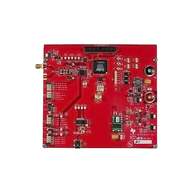
EVM Jumper and Switches
There are many jumpers on the ADS61JBxx EVM to select operational modes of the ADC, power supply
options, and SPI port options. Many of the jumper selections that involve DC inputs or static control
signals are by way of push-on square post jumpers. Figure 3 illustrates the position of the jumpers relative
to the more recognizable features of the EVM, such as the banana jacks or SMA inputs. Jumper
selections that involve high-speed switching signals are implemented by way of surface mount zero-Ω
jumper resistors, represented in Figure 4. In both figures, the default jumper positions are indicated as the
EVM is normally shipped. Note that some of the jumpers are left open circuit, by default. The surface
mount jumper resistors require soldering to change from default to any other desired configuration.
The functions of the connectors, LEDs and pushbutton switches are described by their labels in Figure 2.
LEDs D4, D5, D6, and D7 are lit to show the presence of the supply voltages to the EVM and to the ADC.
LED D8 indicates that the FPGA has loaded its bit file from the EEPROM. LEDs D9 and D10 are reserved
for future use.
SLAU449A – August 2012 – Revised September 2013
Submit Documentation Feedback
Copyright © 2012–2013, Texas Instruments Incorporated
ADS61JBxx EVM User’s Guide
3
�Overview
www.ti.com
J12
GND
PWR IN
JP32
D6
JP16
Reset
FPGA
1
D4
D5
AVDD
DVDD
JP21
JP19
JP31
1
SW3
JP33
Buffer
VDD
JP15
JP18
1 1
SW4 SYNC
JP34
SW2 Program
FPGA
JP17
J10
1
1
D8
D10
J20
D9
JTAG
JP29
rsvd
rsvd
FPGA
BRIDGE
J19
CLKIN
J14
LVD
LVD
Digital Data To TSW1200
FPGA
Ready
J8
JP20
1
USB
Reset
ADC
J27
1
AIN +
J3
AIN J9
DNI
1
J29
1
JP11
J28
1
1
JP10
J13
SW1
JP21
D7
JP9
1
JP8
1
JP5
JP6
ADS61JBxx
J30
1
1
1
1
Figure 3. EVM Jumpers and Switches
4
ADS61JBxx EVM User’s Guide
SLAU449A – August 2012 – Revised September 2013
Submit Documentation Feedback
Copyright © 2012–2013, Texas Instruments Incorporated
�Overview
www.ti.com
There are four pushbutton switches on the EVM. Pushbutton switch SW1 may be used to assert a reset
signal to the ADS61JBxx. The ADS61JBxx requires a reset before it may be configured for use, but it is
not necessary to use the switch (SW1). It is also acceptable to use the ADS61JBxx SPI GUI to toggle the
reset register bit in the ADS61JBxx register map.
The remaining pushbutton switches are used by the FPGA. SW2 causes the FPGA to reload its
programming from the on-board flash EEPROM. (As the FPGA loads its programming from memory upon
every power cycle, the use of SW2 is often not necessary.) SW3 is used to reset the serial receivers in the
FPGA.
Note: This is necessary after every disruption of the serial link.
That is, after every power cycle or disruption of the sample clock, the FPGA receivers must be reset by
pressing SW3. SW4 causes the FPGA to assert the SYNC signal back to the ADS61JBxx, which in turn
causes the ADS61JBxx to send a special synchronization pattern on the serial lines letting the receiver
find byte-alignment to the sample boundaries on the serial lines.
Note: After every assertion of SW3, SW4 must be asserted as well.
To summerize, the usual sequence to bring up the EVM after power is applied, is to reset the ADC by
either SW1 or by the SPI GUI, followed by processing SW3 and then SW4. After every disruption of the
clock to the EVM, press SW3 and then SW4.
SLAU449A – August 2012 – Revised September 2013
Submit Documentation Feedback
Copyright © 2012–2013, Texas Instruments Incorporated
ADS61JBxx EVM User’s Guide
5
�Overview
www.ti.com
J12
GND
J10
PWR IN
D6
D8
D5
SW3
SW4
SW2
D4
D10 D9
LVDS
J8
J19
C73
C78
CLKIN
USB
Power
R123
R105
R108
R120
R121
R107
R106
R122
C44
C62
LVDS
FPGA
BRIDGE
ADS61JBxx
R70
R47
SEN
AIN J9
DNI
R68
R33
AIN +
J3
SDATA
R70
R47
SCLK
D7
SW1
R30
R69
USB
J13
Figure 4. EVM Solder Options
Table 1 lists the jumper options of the EVM by category, along with the default position of the jumper and
a description of what the jumper does in the possible positions that the jumper might be set. Three pin
jumpers have an indication of pin 1 position both in Figure 2 and in the silkscreen on the top of the EVM
itself. A jumper installed between pins 1 and 2 is designated by 1-2 while a jumper installed between pins
2 and 3 is designated by 2-3. Silkscreen on the top of the EVM indicates the position of the jumpers. For
more detailed information on the function of each jumper position, see the ADS61JB23 data sheet
(SLOS755) or the ADS61JB46 data sheet (SBAS611).
6
ADS61JBxx EVM User’s Guide
SLAU449A – August 2012 – Revised September 2013
Submit Documentation Feedback
Copyright © 2012–2013, Texas Instruments Incorporated
�Overview
www.ti.com
For the power supply jumpers, note that the jumpers used to select between the DC-DC regulator or the
LDO regulator must be moved in pairs. If jumper JP17 is set to route power to the DC-DC regulator, then
jumper JP19 must also be set to connect the DC-DC regulator to the ADS61JBxx supplies or the ADC will
not receive power.
Table 1. Square Post Jumpers
Jumper
Default
Description
JP17
open
JP16
1-2
Selects source on 5.3-V supply rail – DC-DC converter or J10 banana jack
JP19
2-3
Selects source of 5-V supply (1-2 J10 red banana jack) (2-3 from 5.3-V internal supply)
JP15
1-2
Connects 1.8 V to ADS61JBxx AVDD analog supply
JP18
1-2
Connects 1.8 V to ADS61JBxx DVDD digital supply
JP21
1-2
Connects 3.3 V to ADS61JBxx input buffer supply
JP29
open
Inhibit the 1.2-V digital supply to the FPGA, when connected
JP5
1-2
Power Down (1-2 = Normal Operation) (2-3 = Power Down)
JP6
1-2
Power Down Analog Circuitry (1-2 = Normal Operation) (2-3 = Power Down)
JP8
1-2
SCLK source (1-2 = SCLK from J28) (2-3 = SCLK driven as SPI Clock)
JP9
1-2
SDATA source (1-2 = SDATA tied high) (2-3 = SDATA driven as SPI Data)
JP10
1-2
SEN Source (1-2 = SEN from J30) (2-3 = SEN driven as SPI Enable)
JP11
2-3
Reset Source (1-2 = Reset from SW1) (2-3 = Reset driven by USB Port)
J27
1-2
DFS Selection (1-2 = DFS 0 V) (3-4 = DFS 3 or 8 AVDD)
(5-6 = DFS 5/8 AVDD) (7-8 = DFS AVDD)
J28
1-2
SCLK Selection (1-2 = SCLK 0 V) (3-4 = SCLK 3 or 8 AVDD)
(5-6 = SCLK 5/8 AVDD) (7-8 = SCLK AVDD)
J29
1-2
Mode1 Selection (1-2 = MODE1 0 V) (3-4 = MODE1 3 or 8 AVDD)
(5-6 = MODE1 5/8 AVDD) (7-8 = MODE1 AVDD)
J30
open
JP30
1-2
Power Supply
Connects J10 red banana jack to DC-DC converter to generate 5.3 V
ADC CONTROL PINS
J31
SEN Selection (1-2 = SEN 0 V) (3-4 = SEN 3 or 8 AVDD)
(5-6 = SEN 5/8 AVDD) (7-8 = SEN AVDD)
SDOUT Connects SDOUT to J32
Gnd pin. Located in such a way to easily let SDATA JP9 be jumpered to ground
USB Port Power
JP20
2-3
IO supply selection (1-2 power from USB port) (2-3 power from EVM)
J20
open
JTAG header for FPGA programming and debugging
JP31
open
Reserved for rate selection
JP32
open
Reserved for rate selection
JP33
open
Reserved
JP34
open
Scrambling (open = normal data format) (jumpered = scrambled format)
FPGA Control
Surface mount zero-Ω resistor jumpers are described in Table 2. The four SPI lines to the ADC (SCLK,
SEN, SDATA, and SDO) are driven by the USB port on the EVM under the control of the ADS61JBxx SPI
GUI software, by default. Alternatively, the TSW1200 Capture Card and its user interface may be used to
perform SPI writes to the ADC, in which case, four surface mount resistors must be removed from their
default positions and soldered in the alternate positions.
The ADS61JBxx has a VCM pin that outputs a common mode voltage which may be used to bias the
common mode level of the analog input. Since the ADS61JBxx has a buffered analog input and the input
signal is internally biased to VCM if the signal is AC coupled, the VCM pin is unconnected, by default. A
zero-Ω jumper resistor may be installed to connect the VCM to the analog input termination network.
SLAU449A – August 2012 – Revised September 2013
Submit Documentation Feedback
Copyright © 2012–2013, Texas Instruments Incorporated
ADS61JBxx EVM User’s Guide
7
�Overview
www.ti.com
Many of the surface mount components listed in Table 2 are used to select whether the serialized data
outputs are to be connected to the connector or to the FPGA, as well as whether the serial pairs are to be
AC coupled or DC coupled. Figure 5 shows the options available, showing just one of the available two
signal pairs. The default connection is to DC couple (with zero-Ω resistors) the CML (Current Mode Logic)
serial outputs from the ADS61JBxx to the serial receivers of the FPGA. The FPGA then provides
termination of the transmission line as well as the pull-up path to supply that the CML output drivers
require. This is the simplest connection. If the FPGA is not to be used to reformat the sample data for the
TSW1200 or TSW1400, then the zero-Ω resistors may be moved from their default location and instead
soldered to connect the CML outputs to the EVM output connector J8. It is also possible to use AC
coupling caps instead of zero-Ω jumper resistors, in which case the CML drivers will now require an
additional 50-Ω pull-up resistor at the output pins of the CML driver. Figure 5 shows the provisions made
on the EVM for all these options.
Vdd
Connector
DNI
DNI
50
50
J8
DNI
Vdd
50
50
0
CML
FPGA
0
DNI
Figure 5. CML Termination Options
Table 2. Surface Mount Jumpers
Jumper
Default
Description
R57
open
Connects VCM to transformer termination mid-point
R70
open
Connects SEN to TSW1200, TSW1400
R47
installed
Connects SEN to USB port on ADS61JBxx EVM
R33
installed
Connects SDATA to USB port on ADS61JBxx EVM
R68
open
R30
installed
R69
open
R118
open
Connects SDATA to TSW1200, TSW1400
Connects SCLK to USB port on ADS61JBxx EVM
Connects SCLK to TSW1200, TSW1400
Connects SDO to TSW1200, TSW1400
Analog Input Channel Single Ended vs. Differential Option
R77
open
Connects SMA input to transformer primary negative side (differential input)
R78
installed
Connects input transformer primary negative side to ground (single ended input)
R120
installed
Connects Channel A Lane 0 positive to FPGA
CML Serial Coupling and Termination Options
8
C44
open
R121
Installed
C62
open
R122
installed
Connects Channel A Lane 0 positive to Connector
Connects Channel A Lane 0 negative to FPGA
Connects Channel A Lane 0 negative to Connector
Connects Channel A Lane 1 positive to FPGA
C73
open
R123
Installed
C78
open
Connects Channel A Lane 1 negative to Connector
R108
open
Pullup Resistor Channel A Lane 0 positive
R107
open
Pullup Resistor Channel A Lane 0 negative
R106
open
Pullup Resistor Channel A Lane 1 positive
R105
open
Pullup Resistor Channel A Lane 1 negative
ADS61JBxx EVM User’s Guide
Connects Channel A Lane 1 positive to Connector
Connects Channel A Lane 1 negative to FPGA
SLAU449A – August 2012 – Revised September 2013
Submit Documentation Feedback
Copyright © 2012–2013, Texas Instruments Incorporated
�Software Control
www.ti.com
2
Software Control
2.1
Installation Instructions
•
•
•
•
•
2.2
Open the folder named ADS61JBxx_Installer_vxpx (xpx represents the latest version, currently 1.2).
Run Setup.exe
Follow the on-screen instructions.
Once installed, launch by clicking on the ADS61JBxx_GUI_vxpx program in Start→Texas Instruments
ADCs
When plugging in the USB cable for the first time, the user is prompted by the Found-New-HardwareWizard to install the USB drivers.
– When a pop-up screen opens, select “Continue Downloading”.
– Follow the on-screen instructions to install the USB drivers.
– If needed, the user can access the drivers directly in the install directory.
Software Operation
The software allows programming control of the ADC device. The front panel provides a tab for full
programming of the register map of the ADS61JBxx and an advanced tab that allows for custom register
accesses. The GUI tabs provide a convenient and simplified interface to the most-used registers of the
device.
2.2.1
Control Options
Figure 6. Control Options
SLAU449A – August 2012 – Revised September 2013
Submit Documentation Feedback
Copyright © 2012–2013, Texas Instruments Incorporated
ADS61JBxx EVM User’s Guide
9
�Software Control
2.2.2
www.ti.com
Register Control
• Send All:
• Read All:
• Save Regs:
• Load Regs:
o
o
o
o
2.2.3
Sends the register configuration to all devices
Reads register configuration from the ADS61JBxx device
(NOTE: Not implemented in version 1.2)
Saves the register configuration for all devices
Load a register file for all devices. Sample configuration files for common
frequency plans are located in the install directory.
Select Load Regs button
Double click on the data folder
Double click on the desired register file
Click the Send All button to ensure all of the values are loaded properly
Misc Settings
• Reset USB
Port:
• Exit:
10
ADS61JBxx EVM User’s Guide
Toggle this button if the USB port is not responding. This generates
a new USB handle address.
Note: Resetting the board and clicking the Reset USB Port button is
recommended after every power cycle.
Stops the program
SLAU449A – August 2012 – Revised September 2013
Submit Documentation Feedback
Copyright © 2012–2013, Texas Instruments Incorporated
�Basic Test Procedure
www.ti.com
3
Basic Test Procedure
This section outlines the basic test procedure for testing the EVM. TSW1200 is shown in Figure 7,
although TSW1400 or TSW1405 provide a newer and more full-featured capture system.
3.1
Test Block Diagram
The test set-up for evaluation of the EVM with the TSW1200 Capture Card is shown in Figure 7. This
figure is the initial setup screen from the TSW1200 User Interface itself. As seen in this figure, the
evaluation setup involves a clock from a high quality signal generator and a sine wave for the analog input
from a high quality signal generator. High order, narrow bandpass filters are usually required on clock and
input frequency to remove phase noise and harmonic content from the input sine waves. If the two signal
generators are not synchronized by an external reference signal to make the clock and input frequency
coherent, then the resulting FFT first needs to have a windowing function such as Hanning or BlackmanHarris applied to the data in the Capture Card GUI.
Figure 7. Test Setup Block Diagram
SLAU449A – August 2012 – Revised September 2013
Submit Documentation Feedback
Copyright © 2012–2013, Texas Instruments Incorporated
ADS61JBxx EVM User’s Guide
11
�Basic Test Procedure
3.2
Test Set-up Connection
•
•
•
•
•
•
•
3.3
www.ti.com
Connect J8 connector of ADS61JBxx EVM to TSW1200 EVM or TSW1400 EVM.
Connect 5 V to the supply input of the ADS61JBxx EVM and to supply the Capture Card.
Provide sample clock at J1 of the ADS61JBxx EVM.
Provide analog input sine wave to Channel A on J4.
Connect USB cable from the TSW1200 to the programming computer.
Connect USB cable from the ADS61JBxx to the computer if the ADS61JBxx SPI GUI is to be used.
Make sure the following jumpers at their default setting.
– J11 of TSW1200 set HI to choose parallel DDR LVDS data format if using TSW1200
– Initial jumper setting of ADS61JBxx as per Table 1 (if default usage of the ADC is desired).
ADS61JBxx Software Quick Start Guide
Figure 6 introduced the front panel of the ADS61JBxx SPI GUI. This section covers the initial use of the
SPI GUI necessary for most evaluations of the ADS61JBxx.
• Press Reset USB Port if the USB connection has been disrupted since last use, or if an error message
pops up warning that the USB connection is not valid.
• Use the mouse to select the ‘reset’ position of the reset switch. This switch is self-clearing.
• Press Send All to send any special register writes that may be pre-stored in the Advanced tab.
• On the ADS61JBxx EVM press the SW3 pushbutton switch (resets the FPGA receivers).
• On the ADS61JBxx EVM press the SW4 pushbutton switch (Asserts SYNC input to ADS61JBxx).
• From this point, select digital functions as desired such as test pattern modes if desired. All register
bits listed in the register map of the ADS61JBxx data sheet have a ‘switch’ on the front panel of the
SPI GUI for easy configuration of the ADS61JBxx.
NOTE: Some of the front panel switches may be ‘greyed out’ and unavailable for use. These
functions must first be enabled by selection of a different switch, as indicated in the
ADS61JB23 or ADS61JB46 data sheet. For example, the octets or frame selection is
unavailable because the default state of the CTRL_F switch is off. Select the CTRL_F switch
to toggle the switch to the enabled state, and then the octets or frame selection becomes
available for use.
12
ADS61JBxx EVM User’s Guide
SLAU449A – August 2012 – Revised September 2013
Submit Documentation Feedback
Copyright © 2012–2013, Texas Instruments Incorporated
�Basic Test Procedure
www.ti.com
3.4
TSW1200 Quick Start Operation
Reference the TSW1200 User’s Guide for more detailed explanations of the TSW1200 set-up and
operation. This document assumes the TSW1200 software is installed and functioning properly. The
ADS61JBxx needs TSW1200 operating software version 1.2 or higher with Rev B (or higher) of TSW1200
board.
Single tone FFT test:
• Select the ADS61JBxx as the TI ADC Device Selection. If this device does not appear in the device
selection, then the initialization file ADS61JBxx.ini is missing from the ADC Files folder where the
TSW1200 User Interface was installed. Close the TSW1200 GUI, copy the ADS61JBxx.ini file into the
ADC Files folder and relaunch the TSW1200 GUI.
• Select Single Tone FFT Test.
• Select number of sample points (and resulting number of FFT bins) to be used.
• Enter the ADC Sampling rate.
• Enter the input frequency desired. If the clock and input frequency signal generators are synchronized,
then make sure the checkbox for coherent frequency is checked and set the input frequency signal
generator to the input frequency displayed.
• Press the Capture button.
• Observe an FFT result similar to that of Figure 8.
If the basic capture at this point is correct, then the front panel options of the SPI GUI and the front panel
options of the TSW1200 GUI may be varied as desired.
Figure 8. TSW1200 FFT Result
SLAU449A – August 2012 – Revised September 2013
Submit Documentation Feedback
Copyright © 2012–2013, Texas Instruments Incorporated
ADS61JBxx EVM User’s Guide
13
�EVALUATION BOARD/KIT/MODULE (EVM) ADDITIONAL TERMS
Texas Instruments (TI) provides the enclosed Evaluation Board/Kit/Module (EVM) under the following conditions:
The user assumes all responsibility and liability for proper and safe handling of the goods. Further, the user indemnifies TI from all claims
arising from the handling or use of the goods.
Should this evaluation board/kit not meet the specifications indicated in the User’s Guide, the board/kit may be returned within 30 days from
the date of delivery for a full refund. THE FOREGOING LIMITED WARRANTY IS THE EXCLUSIVE WARRANTY MADE BY SELLER TO
BUYER AND IS IN LIEU OF ALL OTHER WARRANTIES, EXPRESSED, IMPLIED, OR STATUTORY, INCLUDING ANY WARRANTY OF
MERCHANTABILITY OR FITNESS FOR ANY PARTICULAR PURPOSE. EXCEPT TO THE EXTENT OF THE INDEMNITY SET FORTH
ABOVE, NEITHER PARTY SHALL BE LIABLE TO THE OTHER FOR ANY INDIRECT, SPECIAL, INCIDENTAL, OR CONSEQUENTIAL
DAMAGES.
Please read the User's Guide and, specifically, the Warnings and Restrictions notice in the User's Guide prior to handling the product. This
notice contains important safety information about temperatures and voltages. For additional information on TI's environmental and/or safety
programs, please visit www.ti.com/esh or contact TI.
No license is granted under any patent right or other intellectual property right of TI covering or relating to any machine, process, or
combination in which such TI products or services might be or are used. TI currently deals with a variety of customers for products, and
therefore our arrangement with the user is not exclusive. TI assumes no liability for applications assistance, customer product design,
software performance, or infringement of patents or services described herein.
REGULATORY COMPLIANCE INFORMATION
As noted in the EVM User’s Guide and/or EVM itself, this EVM and/or accompanying hardware may or may not be subject to the Federal
Communications Commission (FCC) and Industry Canada (IC) rules.
For EVMs not subject to the above rules, this evaluation board/kit/module is intended for use for ENGINEERING DEVELOPMENT,
DEMONSTRATION OR EVALUATION PURPOSES ONLY and is not considered by TI to be a finished end product fit for general consumer
use. It generates, uses, and can radiate radio frequency energy and has not been tested for compliance with the limits of computing
devices pursuant to part 15 of FCC or ICES-003 rules, which are designed to provide reasonable protection against radio frequency
interference. Operation of the equipment may cause interference with radio communications, in which case the user at his own expense will
be required to take whatever measures may be required to correct this interference.
General Statement for EVMs including a radio
User Power/Frequency Use Obligations: This radio is intended for development/professional use only in legally allocated frequency and
power limits. Any use of radio frequencies and/or power availability of this EVM and its development application(s) must comply with local
laws governing radio spectrum allocation and power limits for this evaluation module. It is the user’s sole responsibility to only operate this
radio in legally acceptable frequency space and within legally mandated power limitations. Any exceptions to this are strictly prohibited and
unauthorized by Texas Instruments unless user has obtained appropriate experimental/development licenses from local regulatory
authorities, which is responsibility of user including its acceptable authorization.
For EVMs annotated as FCC – FEDERAL COMMUNICATIONS COMMISSION Part 15 Compliant
Caution
This device complies with part 15 of the FCC Rules. Operation is subject to the following two conditions: (1) This device may not cause
harmful interference, and (2) this device must accept any interference received, including interference that may cause undesired operation.
Changes or modifications not expressly approved by the party responsible for compliance could void the user's authority to operate the
equipment.
FCC Interference Statement for Class A EVM devices
This equipment has been tested and found to comply with the limits for a Class A digital device, pursuant to part 15 of the FCC Rules.
These limits are designed to provide reasonable protection against harmful interference when the equipment is operated in a commercial
environment. This equipment generates, uses, and can radiate radio frequency energy and, if not installed and used in accordance with the
instruction manual, may cause harmful interference to radio communications. Operation of this equipment in a residential area is likely to
cause harmful interference in which case the user will be required to correct the interference at his own expense.
�FCC Interference Statement for Class B EVM devices
This equipment has been tested and found to comply with the limits for a Class B digital device, pursuant to part 15 of the FCC Rules.
These limits are designed to provide reasonable protection against harmful interference in a residential installation. This equipment
generates, uses and can radiate radio frequency energy and, if not installed and used in accordance with the instructions, may cause
harmful interference to radio communications. However, there is no guarantee that interference will not occur in a particular installation. If
this equipment does cause harmful interference to radio or television reception, which can be determined by turning the equipment off and
on, the user is encouraged to try to correct the interference by one or more of the following measures:
• Reorient or relocate the receiving antenna.
• Increase the separation between the equipment and receiver.
• Connect the equipment into an outlet on a circuit different from that to which the receiver is connected.
• Consult the dealer or an experienced radio/TV technician for help.
For EVMs annotated as IC – INDUSTRY CANADA Compliant
This Class A or B digital apparatus complies with Canadian ICES-003.
Changes or modifications not expressly approved by the party responsible for compliance could void the user’s authority to operate the
equipment.
Concerning EVMs including radio transmitters
This device complies with Industry Canada licence-exempt RSS standard(s). Operation is subject to the following two conditions: (1) this
device may not cause interference, and (2) this device must accept any interference, including interference that may cause undesired
operation of the device.
Concerning EVMs including detachable antennas
Under Industry Canada regulations, this radio transmitter may only operate using an antenna of a type and maximum (or lesser) gain
approved for the transmitter by Industry Canada. To reduce potential radio interference to other users, the antenna type and its gain should
be so chosen that the equivalent isotropically radiated power (e.i.r.p.) is not more than that necessary for successful communication.
This radio transmitter has been approved by Industry Canada to operate with the antenna types listed in the user guide with the maximum
permissible gain and required antenna impedance for each antenna type indicated. Antenna types not included in this list, having a gain
greater than the maximum gain indicated for that type, are strictly prohibited for use with this device.
Cet appareil numérique de la classe A ou B est conforme à la norme NMB-003 du Canada.
Les changements ou les modifications pas expressément approuvés par la partie responsable de la conformité ont pu vider l’autorité de
l'utilisateur pour actionner l'équipement.
Concernant les EVMs avec appareils radio
Le présent appareil est conforme aux CNR d'Industrie Canada applicables aux appareils radio exempts de licence. L'exploitation est
autorisée aux deux conditions suivantes : (1) l'appareil ne doit pas produire de brouillage, et (2) l'utilisateur de l'appareil doit accepter tout
brouillage radioélectrique subi, même si le brouillage est susceptible d'en compromettre le fonctionnement.
Concernant les EVMs avec antennes détachables
Conformément à la réglementation d'Industrie Canada, le présent émetteur radio peut fonctionner avec une antenne d'un type et d'un gain
maximal (ou inférieur) approuvé pour l'émetteur par Industrie Canada. Dans le but de réduire les risques de brouillage radioélectrique à
l'intention des autres utilisateurs, il faut choisir le type d'antenne et son gain de sorte que la puissance isotrope rayonnée équivalente
(p.i.r.e.) ne dépasse pas l'intensité nécessaire à l'établissement d'une communication satisfaisante.
Le présent émetteur radio a été approuvé par Industrie Canada pour fonctionner avec les types d'antenne énumérés dans le manuel
d’usage et ayant un gain admissible maximal et l'impédance requise pour chaque type d'antenne. Les types d'antenne non inclus dans
cette liste, ou dont le gain est supérieur au gain maximal indiqué, sont strictement interdits pour l'exploitation de l'émetteur.
SPACER
SPACER
SPACER
SPACER
SPACER
SPACER
SPACER
SPACER
�【Important Notice for Users of EVMs for RF Products in Japan】
】
This development kit is NOT certified as Confirming to Technical Regulations of Radio Law of Japan
If you use this product in Japan, you are required by Radio Law of Japan to follow the instructions below with respect to this product:
1.
2.
3.
Use this product in a shielded room or any other test facility as defined in the notification #173 issued by Ministry of Internal Affairs and
Communications on March 28, 2006, based on Sub-section 1.1 of Article 6 of the Ministry’s Rule for Enforcement of Radio Law of
Japan,
Use this product only after you obtained the license of Test Radio Station as provided in Radio Law of Japan with respect to this
product, or
Use of this product only after you obtained the Technical Regulations Conformity Certification as provided in Radio Law of Japan with
respect to this product. Also, please do not transfer this product, unless you give the same notice above to the transferee. Please note
that if you could not follow the instructions above, you will be subject to penalties of Radio Law of Japan.
Texas Instruments Japan Limited
(address) 24-1, Nishi-Shinjuku 6 chome, Shinjuku-ku, Tokyo, Japan
http://www.tij.co.jp
【無線電波を送信する製品の開発キットをお使いになる際の注意事項】
本開発キットは技術基準適合証明を受けておりません。
本製品のご使用に際しては、電波法遵守のため、以下のいずれかの措置を取っていただく必要がありますのでご注意ください。
1.
2.
3.
電波法施行規則第6条第1項第1号に基づく平成18年3月28日総務省告示第173号で定められた電波暗室等の試験設備でご使用いただく。
実験局の免許を取得後ご使用いただく。
技術基準適合証明を取得後ご使用いただく。
なお、本製品は、上記の「ご使用にあたっての注意」を譲渡先、移転先に通知しない限り、譲渡、移転できないものとします。
上記を遵守頂けない場合は、電波法の罰則が適用される可能性があることをご留意ください。
日本テキサス・インスツルメンツ株式会社
東京都新宿区西新宿6丁目24番1号
西新宿三井ビル
http://www.tij.co.jp
SPACER
SPACER
SPACER
SPACER
SPACER
SPACER
SPACER
SPACER
SPACER
SPACER
SPACER
SPACER
SPACER
SPACER
SPACER
SPACER
SPACER
�EVALUATION BOARD/KIT/MODULE (EVM)
WARNINGS, RESTRICTIONS AND DISCLAIMERS
For Feasibility Evaluation Only, in Laboratory/Development Environments. Unless otherwise indicated, this EVM is not a finished
electrical equipment and not intended for consumer use. It is intended solely for use for preliminary feasibility evaluation in
laboratory/development environments by technically qualified electronics experts who are familiar with the dangers and application risks
associated with handling electrical mechanical components, systems and subsystems. It should not be used as all or part of a finished end
product.
Your Sole Responsibility and Risk. You acknowledge, represent and agree that:
1.
2.
3.
4.
You have unique knowledge concerning Federal, State and local regulatory requirements (including but not limited to Food and Drug
Administration regulations, if applicable) which relate to your products and which relate to your use (and/or that of your employees,
affiliates, contractors or designees) of the EVM for evaluation, testing and other purposes.
You have full and exclusive responsibility to assure the safety and compliance of your products with all such laws and other applicable
regulatory requirements, and also to assure the safety of any activities to be conducted by you and/or your employees, affiliates,
contractors or designees, using the EVM. Further, you are responsible to assure that any interfaces (electronic and/or mechanical)
between the EVM and any human body are designed with suitable isolation and means to safely limit accessible leakage currents to
minimize the risk of electrical shock hazard.
Since the EVM is not a completed product, it may not meet all applicable regulatory and safety compliance standards (such as UL,
CSA, VDE, CE, RoHS and WEEE) which may normally be associated with similar items. You assume full responsibility to determine
and/or assure compliance with any such standards and related certifications as may be applicable. You will employ reasonable
safeguards to ensure that your use of the EVM will not result in any property damage, injury or death, even if the EVM should fail to
perform as described or expected.
You will take care of proper disposal and recycling of the EVM’s electronic components and packing materials.
Certain Instructions. It is important to operate this EVM within TI’s recommended specifications and environmental considerations per the
user guidelines. Exceeding the specified EVM ratings (including but not limited to input and output voltage, current, power, and
environmental ranges) may cause property damage, personal injury or death. If there are questions concerning these ratings please contact
a TI field representative prior to connecting interface electronics including input power and intended loads. Any loads applied outside of the
specified output range may result in unintended and/or inaccurate operation and/or possible permanent damage to the EVM and/or
interface electronics. Please consult the EVM User's Guide prior to connecting any load to the EVM output. If there is uncertainty as to the
load specification, please contact a TI field representative. During normal operation, some circuit components may have case temperatures
greater than 60°C as long as the input and output are maintained at a normal ambient operating temperature. These components include
but are not limited to linear regulators, switching transistors, pass transistors, and current sense resistors which can be identified using the
EVM schematic located in the EVM User's Guide. When placing measurement probes near these devices during normal operation, please
be aware that these devices may be very warm to the touch. As with all electronic evaluation tools, only qualified personnel knowledgeable
in electronic measurement and diagnostics normally found in development environments should use these EVMs.
Agreement to Defend, Indemnify and Hold Harmless. You agree to defend, indemnify and hold TI, its licensors and their representatives
harmless from and against any and all claims, damages, losses, expenses, costs and liabilities (collectively, "Claims") arising out of or in
connection with any use of the EVM that is not in accordance with the terms of the agreement. This obligation shall apply whether Claims
arise under law of tort or contract or any other legal theory, and even if the EVM fails to perform as described or expected.
Safety-Critical or Life-Critical Applications. If you intend to evaluate the components for possible use in safety critical applications (such
as life support) where a failure of the TI product would reasonably be expected to cause severe personal injury or death, such as devices
which are classified as FDA Class III or similar classification, then you must specifically notify TI of such intent and enter into a separate
Assurance and Indemnity Agreement.
Mailing Address: Texas Instruments, Post Office Box 655303, Dallas, Texas 75265
Copyright © 2013, Texas Instruments Incorporated
�IMPORTANT NOTICE
Texas Instruments Incorporated and its subsidiaries (TI) reserve the right to make corrections, enhancements, improvements and other
changes to its semiconductor products and services per JESD46, latest issue, and to discontinue any product or service per JESD48, latest
issue. Buyers should obtain the latest relevant information before placing orders and should verify that such information is current and
complete. All semiconductor products (also referred to herein as “components”) are sold subject to TI’s terms and conditions of sale
supplied at the time of order acknowledgment.
TI warrants performance of its components to the specifications applicable at the time of sale, in accordance with the warranty in TI’s terms
and conditions of sale of semiconductor products. Testing and other quality control techniques are used to the extent TI deems necessary
to support this warranty. Except where mandated by applicable law, testing of all parameters of each component is not necessarily
performed.
TI assumes no liability for applications assistance or the design of Buyers’ products. Buyers are responsible for their products and
applications using TI components. To minimize the risks associated with Buyers’ products and applications, Buyers should provide
adequate design and operating safeguards.
TI does not warrant or represent that any license, either express or implied, is granted under any patent right, copyright, mask work right, or
other intellectual property right relating to any combination, machine, or process in which TI components or services are used. Information
published by TI regarding third-party products or services does not constitute a license to use such products or services or a warranty or
endorsement thereof. Use of such information may require a license from a third party under the patents or other intellectual property of the
third party, or a license from TI under the patents or other intellectual property of TI.
Reproduction of significant portions of TI information in TI data books or data sheets is permissible only if reproduction is without alteration
and is accompanied by all associated warranties, conditions, limitations, and notices. TI is not responsible or liable for such altered
documentation. Information of third parties may be subject to additional restrictions.
Resale of TI components or services with statements different from or beyond the parameters stated by TI for that component or service
voids all express and any implied warranties for the associated TI component or service and is an unfair and deceptive business practice.
TI is not responsible or liable for any such statements.
Buyer acknowledges and agrees that it is solely responsible for compliance with all legal, regulatory and safety-related requirements
concerning its products, and any use of TI components in its applications, notwithstanding any applications-related information or support
that may be provided by TI. Buyer represents and agrees that it has all the necessary expertise to create and implement safeguards which
anticipate dangerous consequences of failures, monitor failures and their consequences, lessen the likelihood of failures that might cause
harm and take appropriate remedial actions. Buyer will fully indemnify TI and its representatives against any damages arising out of the use
of any TI components in safety-critical applications.
In some cases, TI components may be promoted specifically to facilitate safety-related applications. With such components, TI’s goal is to
help enable customers to design and create their own end-product solutions that meet applicable functional safety standards and
requirements. Nonetheless, such components are subject to these terms.
No TI components are authorized for use in FDA Class III (or similar life-critical medical equipment) unless authorized officers of the parties
have executed a special agreement specifically governing such use.
Only those TI components which TI has specifically designated as military grade or “enhanced plastic” are designed and intended for use in
military/aerospace applications or environments. Buyer acknowledges and agrees that any military or aerospace use of TI components
which have not been so designated is solely at the Buyer's risk, and that Buyer is solely responsible for compliance with all legal and
regulatory requirements in connection with such use.
TI has specifically designated certain components as meeting ISO/TS16949 requirements, mainly for automotive use. In any case of use of
non-designated products, TI will not be responsible for any failure to meet ISO/TS16949.
Products
Applications
Audio
www.ti.com/audio
Automotive and Transportation
www.ti.com/automotive
Amplifiers
amplifier.ti.com
Communications and Telecom
www.ti.com/communications
Data Converters
dataconverter.ti.com
Computers and Peripherals
www.ti.com/computers
DLP® Products
www.dlp.com
Consumer Electronics
www.ti.com/consumer-apps
DSP
dsp.ti.com
Energy and Lighting
www.ti.com/energy
Clocks and Timers
www.ti.com/clocks
Industrial
www.ti.com/industrial
Interface
interface.ti.com
Medical
www.ti.com/medical
Logic
logic.ti.com
Security
www.ti.com/security
Power Mgmt
power.ti.com
Space, Avionics and Defense
www.ti.com/space-avionics-defense
Microcontrollers
microcontroller.ti.com
Video and Imaging
www.ti.com/video
RFID
www.ti-rfid.com
OMAP Applications Processors
www.ti.com/omap
TI E2E Community
e2e.ti.com
Wireless Connectivity
www.ti.com/wirelessconnectivity
Mailing Address: Texas Instruments, Post Office Box 655303, Dallas, Texas 75265
Copyright © 2013, Texas Instruments Incorporated
�