ADS62P49 / ADS62P29
ADS62P48 / ADS62P28
www.ti.com
SLAS635B – APRIL 2009 – REVISED JANUARY 2011
Dual Channel 14-/12-Bit, 250-/210-MSPS ADC With DDR LVDS and Parallel CMOS Outputs
Check for Samples: ADS62P49 / ADS62P29, ADS62P48 / ADS62P28
FEATURES
•
1
•
•
•
•
•
•
•
•
Maximum Sample Rate: 250 MSPS
14-Bit Resolution – ADS62P49/ADS62P48
12-Bit Resolution – ADS62P29/ADS62P28
Total Power: 1.25 W at 250 MSPS
Double Data Rate (DDR) LVDS and Parallel
CMOS Output Options
Programmable Gain up to 6dB for SNR/SFDR
Trade-Off
DC Offset Correction
90dB Cross-Talk
•
•
Supports Input Clock Amplitude Down to 400
mVPP Differential
Internal and External Reference Support
64-QFN Package (9 mm × 9 mm)
ADS62Pxx High Speed Family
250 MSPS
210 MSPS
14-Bit Family
ADS62P49
ADS62P48
12-Bit Family
ADS62P29
ADS62P28
11-Bit Family
200 MSPS
ADS62C17
DESCRIPTION
The ADS62Px9/x8 is a family of dual channel 14-bit and 12-bit A/D converters with sampling rates up to 250
MSPS. It combines high dynamic performance and low power consumption in a compact 64 QFN package. This
makes it well-suited for multi-carrier, wide band-width communications applications.
The ADS62Px9/x8 has gain options that can be used to improve SFDR performance at lower full-scale input
ranges. It includes a dc offset correction loop that can be used to cancel the ADC offset. Both DDR LVDS
(Double Data Rate) and parallel CMOS digital output interfaces are available.
It includes internal references while the traditional reference pins and associated decoupling capacitors have
been eliminated. Nevertheless, the device can also be driven with an external reference. The device is specified
over the industrial temperature range (–40°C to 85°C).
Table 1. Performance Summary
AT 170MHZ INPUT
SFDR, dBc
SINAD, dBFS
ADS62P49
ADS62P48
ADS62P29
ADS62P28
0 dB gain
75
78
75
78
6 dB gain
82
84
82
84
0 dB gain
69.8
70.1
68.3
68.7
6 dB gain
66.5
66.3
65.8
65.8
1
0.92
1
0.92
Analog Power, W
1
Please be aware that an important notice concerning availability, standard warranty, and use in critical applications of Texas
Instruments semiconductor products and disclaimers thereto appears at the end of this data sheet.
PRODUCTION DATA information is current as of publication date.
Products conform to specifications per the terms of the Texas
Instruments standard warranty. Production processing does not
necessarily include testing of all parameters.
Copyright © 2009–2011, Texas Instruments Incorporated
�ADS62P49 / ADS62P29
ADS62P48 / ADS62P28
DRGND
DRVDD
www.ti.com
AGND
AVDD
SLAS635B – APRIL 2009 – REVISED JANUARY 2011
LVDS INTERFACE
DA0_P/M
DA2_P/M
INA_P
INA_M
Sample
and
Hold
DA4_P/M
Digital
and
DDR
Serializer
14-Bit
ADC
DA6_P/M
DA8_P/M
DA10_P/M
DA12_P/M
CLKP
CLKM
Output
Clock
Buffer
CLOCKGEN
CLKOUTP/M
DB0_P/M
DB2_P/M
INB_P
INB_M
Sample
and
Hold
DB4_P/M
Digital
and
DDR
Serializer
14-Bit
ADC
DB6_P/M
DB8_P/M
DB10_P/M
DB12_P/M
VCM
Control Interface
Reference
SDOUT
CTRL1
CTRL2
CTRL3
SCLK
SEN
SDATA
RESET
ADS62P49/48
B0349-01
Figure 1. ADS62P49/48 Block Diagram
2
Submit Documentation Feedback
Copyright © 2009–2011, Texas Instruments Incorporated
Product Folder Link(s): ADS62P49 / ADS62P29 ADS62P48 / ADS62P28
�ADS62P49 / ADS62P29
ADS62P48 / ADS62P28
DRGND
AGND
DRVDD
SLAS635B – APRIL 2009 – REVISED JANUARY 2011
AVDD
www.ti.com
LVDS INTERFACE
DA0_P/M
DA2_P/M
INA_P
INA_M
Sample
and
Hold
DA4_P/M
Digital
and
DDR
Serializer
12-Bit
ADC
DA6_P/M
DA8_P/M
DA10_P/M
CLKP
CLKM
Output
Clock
Buffer
CLOCKGEN
CLKOUTP/M
DB0_P/M
DB2_P/M
INB_P
INB_M
Sample
and
Hold
DB4_P/M
Digital
and
DDR
Serializer
12-Bit
ADC
DB6_P/M
DB8_P/M
DB10_P/M
VCM
Control Interface
Reference
SDOUT
CTRL1
CTRL2
CTRL3
SCLK
SEN
SDATA
RESET
ADS62P29/28
B0350-01
Figure 2. ADS62P29/28 Block Diagram
Copyright © 2009–2011, Texas Instruments Incorporated
Submit Documentation Feedback
Product Folder Link(s): ADS62P49 / ADS62P29 ADS62P48 / ADS62P28
3
�ADS62P49 / ADS62P29
ADS62P48 / ADS62P28
SLAS635B – APRIL 2009 – REVISED JANUARY 2011
www.ti.com
PACKAGE/ORDERING INFORMATION (1)
PRODUCT
PACKAGELEAD
PACKAGE
DESIGNATOR
SPECIFIED
TEMPERATURE
RANGE
ECO
PLAN (2)
LEAD/BALL
FINISH
ADS62P49
ADS62P48
QFN-64
RGC
–40°C to 85°C
ADS62P29
GREEN
(RoHS and
no Sb/Br)
(2)
ORDERING
NUMBER
AZ62P49
ADS62P49IRGCT,
ADS62P49IRGCR
AZ62P48
ADS62P48IRGCT,
ADS62P48IRGCR
AZ62P29
ADS62P29IRGCT,
ADS62P29IRGCR
AZ62P28
ADS62P28IRGCT,
ADS62P28IRGCR
Cu NiPdAu
ADS62P28
(1)
PACKAGE
MARKING
TRANSPORT
MEDIA,QUANTITY
Tape and Reel
Tape and Reel
For the most current product and ordering information, see the Package Option Addendum at the end of this document, or see the TI
web site at www.ti.com.
Eco Plan – The planned eco-friendly classification: Green (RoHS and no Sb/Br): TI defines “Green” to mean Pb-Free (RoHS compatible)
and free of Bromine (Br) and Antimony (Sb) based flame retardants.
ABSOLUTE MAXIMUM RATINGS (1)
over operating free-air temperature range (unless otherwise noted)
VALUE
UNIT
Supply voltage range, AVDD
–0.3 V to 3.9
V
Supply voltage range, DRVDD
–0.3 V to 2.2
V
Voltage between AGND and DRGND
–0.3 to 0.3
V
Voltage between AVDD to DRVDD (AVDD leads DRVDD during power
up/DRVDD leads AVDD during power down)
–0.3 to 4.2
V
Voltage between DRVDD to AVDD (DRVDD leads AVDD during power
up/AVDD leads DRVDD during power down)
–2.5 to 1.7
V
Voltage applied to external pin, VCM (in external reference mode)
Voltage applied to analog input pins – INP_A, INM_A, INP_B, INM_B
Voltage applied to input pins - CLKP, CLKM (2), RESET, SCLK, SDATA,
SEN, CTRL1, CTRL2, CTRL3
–0.3 to 2.0
V
–0.3V to minimum ( 3.6, AVDD + 0.3V )
V
–0.3V to AVDD + 0.3V
V
TA
Operating free-air temperature range
–40 to 85
°C
TJ
Operating junction temperature range
125
°C
Tstg Storage temperature range
–65 to 150
°C
2
kV
ESD, human body model
(1)
(2)
4
Stresses beyond those listed under absolute maximum ratings may cause permanent damage to the device. These are stress ratings
only and functional operation of the device at these or any other conditions beyond those indicated under recommended operating
conditions is not implied. Exposure to absolute maximum rated conditions for extended periods may affect device reliability.
When AVDD is turned off, it is recommended to switch off the input clock (or ensure the voltage on CLKP, CLKM is < |0.3V|). This
prevents the ESD protection diodes at the clock input pins from turning on.
Submit Documentation Feedback
Copyright © 2009–2011, Texas Instruments Incorporated
Product Folder Link(s): ADS62P49 / ADS62P29 ADS62P48 / ADS62P28
�ADS62P49 / ADS62P29
ADS62P48 / ADS62P28
www.ti.com
SLAS635B – APRIL 2009 – REVISED JANUARY 2011
THERMAL INFORMATION
ADS62Pxx
THERMAL METRIC (1)
RGC PACKAGE
UNITS
64 PINS
Junction-to-ambient thermal resistance (2)
qJA
23.0
(3)
qJCtop
Junction-to-case (top) thermal resistance
qJB
Junction-to-board thermal resistance (4)
4.2
yJT
Junction-to-top characterization parameter (5)
0.1
yJB
Junction-to-board characterization parameter (6)
4.2
qJCbot
Junction-to-case (bottom) thermal resistance (7)
0.57
(1)
(2)
(3)
(4)
(5)
(6)
(7)
10.5
°C/W
For more information about traditional and new thermal metrics, see the IC Package Thermal Metrics application report, SPRA953.
The junction-to-ambient thermal resistance under natural convection is obtained in a simulation on a JEDEC-standard, high-K board, as
specified in JESD51-7, in an environment described in JESD51-2a.
The junction-to-case (top) thermal resistance is obtained by simulating a cold plate test on the package top. No specific
JEDEC-standard test exists, but a close description can be found in the ANSI SEMI standard G30-88.
The junction-to-board thermal resistance is obtained by simulating in an environment with a ring cold plate fixture to control the PCB
temperature, as described in JESD51-8.
The junction-to-top characterization parameter, yJT, estimates the junction temperature of a device in a real system and is extracted
from the simulation data for obtaining qJA, using a procedure described in JESD51-2a (sections 6 and 7).
The junction-to-board characterization parameter, yJB, estimates the junction temperature of a device in a real system and is extracted
from the simulation data for obtaining qJA , using a procedure described in JESD51-2a (sections 6 and 7).
The junction-to-case (bottom) thermal resistance is obtained by simulating a cold plate test on the exposed (power) pad. No specific
JEDEC standard test exists, but a close description can be found in the ANSI SEMI standard G30-88.
Copyright © 2009–2011, Texas Instruments Incorporated
Submit Documentation Feedback
Product Folder Link(s): ADS62P49 / ADS62P29 ADS62P48 / ADS62P28
5
�ADS62P49 / ADS62P29
ADS62P48 / ADS62P28
SLAS635B – APRIL 2009 – REVISED JANUARY 2011
www.ti.com
RECOMMENDED OPERATING CONDITIONS
MIN
TYP
MAX
UNIT
SUPPLIES
AVDD
Analog supply voltage
3.15
3.3
3.6
V
DRVDD
Digital supply voltage
1.7
1.8
1.9
V
ANALOG INPUTS
Differential input voltage range
2
Input common-mode voltage
1.5 ±0.1
Voltage applied on CM in external reference mode
1.5±0.05
VPP
V
V
Maximum analog input frequency with 2 Vpp input amplitude (1)
500
MHz
Maximum analog input frequency with 1 Vpp input amplitude (1)
800
MHz
CLOCK INPUT
Input clock sample rate
ADS62P49 / ADS62P29
ADS62P48 / ADS62P28
Enable low speed mode (2)
Low speed mode disabled (default mode after reset)
1
80
>80
250 (3)
Enable low speed mode (2)
Low speed mode disabled (default mode after reset)
1
80
>80
210
1
65
With multiplexed mode enabled (4)
Input clock amplitude differential (VCLKP–VCLKM)
MSPS
MSPS
MSPS
(5) (6)
Sine wave, ac-coupled
1.5
VPP
LVPECL, ac-coupled
0.2
1.6
VPP
LVDS, ac-coupled
0.7
VPP
LVCMOS, single-ended, ac-coupled
3.3
Input clock duty cycle
40%
50%
V
60%
DIGITAL OUTPUTS
CLOAD
Maximum external load capacitance from each output pin to DRGND
RLOAD
Differential load resistance between the LVDS output pairs (LVDS mode)
TA
Operating free-air temperature
(1)
(2)
(3)
(4)
(5)
(6)
5
pF
Ω
100
–40
85
°C
See the Theory of Operation section for information.
Use register bit , refer to the Serial Register Map section for information.
With LVDS interface only; maximum recommended sample rate with CMOS interface is 210 MSPS.
See the Multiplexed Output Mode section for information.
Refer to Performance vs Input Clock Amplitude Chart on Figure 35, Figure 52, Figure 69, and Figure 86.
Refer to Figure 3 for the definition of clock amplitude.
VCLKP - VCLKM
Vp
0
Vpp
Figure 3. Clock Amplitude Definition Diagram
6
Submit Documentation Feedback
Copyright © 2009–2011, Texas Instruments Incorporated
Product Folder Link(s): ADS62P49 / ADS62P29 ADS62P48 / ADS62P28
�ADS62P49 / ADS62P29
ADS62P48 / ADS62P28
www.ti.com
SLAS635B – APRIL 2009 – REVISED JANUARY 2011
ELECTRICAL CHARACTERISTICS – ADS62P49/48 and ADS62P29/28
Typical values are at 25°C, AVDD = 3.3V, DRVDD = 1.8V, 50% clock duty cycle, –1dBFS differential analog input, internal
reference mode (unless otherwise noted).
Min and max values are across the full temperature range TMIN = –40°C to TMAX = 85°C, AVDD = 3.3V, DRVDD = 1.8V
PARAMETER
ADS62P49/ADS62P29
250 MSPS
MIN
TYP
ADS62P48/ADS62P28
210 MSPS
MAX
MIN
TYP
UNIT
MAX
ANALOG INPUT
Differential input voltage range (0 dB gain)
2
2
Vpp
Differential input resistance (at dc), See Figure 100
>1
>1
MΩ
Differential input capacitance, See Figure 101
3.5
3.5
pF
Analog input bandwidth (with 25Ω source impedance)
700
700
MHz
Analog Input common mode current (per channel)
3.6
3.6
mA/MSPS
VCM
Common mode output voltage
1.5
1.5
V
VCM
Output current capability
±4
±4
mA
DC ACCURACY
Offset error
–20
Temperature coefficient of offset error
Variation of offset error with supply
±2
20
–20
±2
20
mV
0.02
0.02
mV/ °C
0.5
0.5
mV/V
There are two sources of gain error – internal reference
inaccuracy and channel gain error.
EGREF
Gain error due to internal reference inaccuracy alone
–1
±0.2
1
–1
±0.2
1
EGCHAN
Gain error of channel alone (1)
–1
±0.2
1
–1
±0.2
1
Temperature coefficient of EGCHAN
Gain
matching
(2)
0.002
% FS
% FS
Δ% /°C
0.002
Difference in gain errors between two channels
within the same device
–2
2
–2
2
Difference in gain errors between two channels
across two devices
–4
4
–4
4
% FS
POWER SUPPLY
IAVDD
Analog supply current
305
350
280
320
mA
IDRVDD
Output buffer supply current, LVDS interface with 100 Ω
external termination
133
175
122
165
mA
IDRVDD
Output buffer supply current, CMOS interface, Fin = 2MHz,
No external load capacitance (3) (4)
(4)
91
mA
Analog power
1.01
1.15
0.92
Digital power, LVDS interface
0.24
0.315
0.22
0.3
W
45
100
45
100
mW
Global power down
(1)
(2)
(3)
–
1.05
W
This is specified by design and characterization; it is not tested in production.
For two channels within the same device, only the channel gain error matters, as the reference is common for both channels.
In CMOS mode, the DRVDD current scales with the sampling frequency, the load capacitance on output pins, input frequency and the
supply voltage (see Figure 92 and CMOS interface power dissipation in application section).
The maximum DRVDD current with CMOS interface depends on the actual load capacitance on the digital output lines. Note that the
maximum recommended load capacitance on each digital output line is 10 pF.
Copyright © 2009–2011, Texas Instruments Incorporated
Submit Documentation Feedback
Product Folder Link(s): ADS62P49 / ADS62P29 ADS62P48 / ADS62P28
7
�ADS62P49 / ADS62P29
ADS62P48 / ADS62P28
SLAS635B – APRIL 2009 – REVISED JANUARY 2011
www.ti.com
ELECTRICAL CHARACTERISTICS – ADS62P49/48
Typical values are at 25°C, AVDD = 3.3V, DRVDD = 1.8V, 50% clock duty cycle, –1dBFS differential analog input, 0 dB gain,
internal reference mode (unless otherwise noted).
Min and max values are across the full temperature range TMIN = –40°C to TMAX = 85°C, AVDD = 3.3V, DRVDD = 1.8V
PARAMETER
TEST CONDITIONS
ADS62P49
250 MSPS
MIN
SNR
Signal to noise ratio,
LVDS
MAX
MIN
TYP
Fin= 20 MHz
73.4
73.4
Fin = 60 MHz
73
73
Fin = 100 MHz
72
Fin = 170 MHz
SINAD
Signal to noise and distortion ratio,
LVDS
TYP
ADS62P48
210 MSPS
0 dB gain
68
72
71
68
66.6
66.4
69.8
69.7
Fin= 20 MHz
73.2
73
Fin = 60 MHz
72.7
72.8
Fin = 100 MHz
71.2
0 dB gain
66.5
6 dB gain
dBFS
71
Fin = 230 MHz
Fin = 170 MHz
6 dB gain
UNIT
MAX
71.5
69.8
66.5
dBFS
70.1
66.5
66.3
Fin = 230 MHz
69
68
ENOB,
Effective number of bits
Fin = 170 MHz
11.3
11.4
DNL
Differential non-linearity
Fin = 170 MHz
–0.95
±0.6
1.3
–0.95
±0.6
1.3
LSB
INL
Integrated non-linearity
Fin = 170 MHz
–5
±2.5
5
–5
±2.5
5
LSB
LSB
ELECTRICAL CHARACTERISTICS – ADS62P29/28
Typical values are at 25°C, AVDD = 3.3V, DRVDD = 1.8V, 50% clock duty cycle, –1dBFS differential analog input, 0 dB gain,
internal reference mode (unless otherwise noted).
Min and max values are across the full temperature range TMIN = –40°C to TMAX = 85°C, AVDD = 3.3V, DRVDD = 1.8V
PARAMETER
TEST CONDITIONS
ADS62P29
250 MSPS
MIN
SNR
Signal to noise ratio,
LVDS
ENOB,
Effective number of bits
MAX
MIN
TYP
Fin= 20 MHz
70.7
70.8
Fin = 60 MHz
70.5
70.6
Fin = 100 MHz
69.8
Fin = 170 MHz
SINAD
Signal to noise and distortion ratio,
LVDS
TYP
ADS62P28
210 MSPS
0 dB gain
66.5
70
69.4
66.5
66
65.9
68.4
68.4
Fin= 20 MHz
70.6
70.6
Fin = 60 MHz
70.3
70.5
Fin = 100 MHz
69.3
0 dB gain
66
6 dB gain
dBFS
69.4
Fin = 230 MHz
Fin = 170 MHz
6 dB gain
UNIT
MAX
69.7
68.3
66
dBFS
68.7
65.9
65.8
Fin = 230 MHz
67.9
67.1
Fin = 170 MHz
11
11.1
LSB
DNL
Differential non-linearity
–0.9
±0.2
1.3
–0.9
±0.2
1.3
LSB
INL
Integrated non-linearity
–5
±1
5
–5
±1
5
LSB
8
Submit Documentation Feedback
Copyright © 2009–2011, Texas Instruments Incorporated
Product Folder Link(s): ADS62P49 / ADS62P29 ADS62P48 / ADS62P28
�ADS62P49 / ADS62P29
ADS62P48 / ADS62P28
www.ti.com
SLAS635B – APRIL 2009 – REVISED JANUARY 2011
ELECTRICAL CHARACTERISTICS – ADS62P49/48
Typical values are at 25°C, AVDD = 3.3V, DRVDD = 1.8V, 50% clock duty cycle, –1dBFS differential analog input, 0 dB gain,
internal reference mode (unless otherwise noted).
Min and max values are across the full temperature range TMIN = –40°C to TMAX = 85°C, AVDD = 3.3V, DRVDD = 1.8V
PARAMETER
TEST CONDITIONS
ADS62P49/ADS62P29
250 MSPS
MIN
SFDR
Spurious Free Dynamic Range
85
85
85
Fin = 100 MHz
78
71
71
77
72
98
98
Fin = 60 MHz
95
95
92
92
90
78
90
90
Fin= 20 MHz
93
95
Fin = 60 MHz
90
94
Fin = 100 MHz
90
90
85
71
85
80
Fin= 20 MHz
89
85
Fin = 60 MHz
85
85
Fin = 170 MHz
78
71
Fin = 230 MHz
80
75
71
72
Fin= 20 MHz
87
83.5
Fin = 60 MHz
83.5
84.6
Fin = 100 MHz
77.5
70
74
79.7
70.5
dBc
77
77
Fin = 170 MHz
dBc
88
Fin = 230 MHz
Fin = 100 MHz
dBc
91
Fin = 230 MHz
71
dBc
77
Fin= 20 MHz
77
UNIT
MAX
80
75
Fin = 230 MHz
Fin = 170 MHz
THD
Total harmonic distortion
TYP
89
Fin = 170 MHz
HD3
Third Harmonic Distortion
MIN
Fin = 60 MHz
Fin = 100 MHz
HD2
Second Harmonic Distortion
MAX
Fin= 20 MHz
Fin = 170 MHz
SFDR
Spurious Free Dynamic Range,
excluding HD2,HD3
TYP
ADS62P48/ADS62P28
210 MSPS
dBc
76.5
Fin = 230 MHz
75
71
F1 = 46 MHz, F2 = 50 MHz,
each tone at –7 dBFS
87
91
F1 = 185 MHz, F2 = 190
MHz,
each tone at –7 dBFS
85
84.5
Cross-talk
Up to 200-MHz cross-talk
frequency
90
90
dB
Input overload recovery
Recovery to within 1% (of final
value) for 6-dB overload with
sine wave input
1
1
Clock
Cycles
PSRR
AC Power supply rejection ratio
For 100-mV pp signal on
AVDD supply
25
25
dB
IMD
2-Tone Inter-modulation Distortion
Copyright © 2009–2011, Texas Instruments Incorporated
dBFS
Submit Documentation Feedback
Product Folder Link(s): ADS62P49 / ADS62P29 ADS62P48 / ADS62P28
9
�ADS62P49 / ADS62P29
ADS62P48 / ADS62P28
SLAS635B – APRIL 2009 – REVISED JANUARY 2011
www.ti.com
DIGITAL CHARACTERISTICS — ADS62Px9/x8
The DC specifications refer to the condition where the digital outputs are not switching, but are permanently at a valid logic
level 0 or 1. AVDD = 3.3V, DRVDD = 1.8V
PARAMETER
ADS62P49/ADS62P48/
ADS62P29/ADS62P28
TEST CONDITIONS
MIN
TYP
UNIT
MAX
DIGITAL INPUTS – CTRL1, CTRL2, CTRL3, RESET, SCLK, SDATA, SEN (1)
High-level input voltage
High-level input current
Low-level input current
1.3
All digital inputs support 1.8V and 3.3V
CMOS logic levels.
Low-level input voltage
SDATA, SCLK (2)
SEN (3)
SDATA, SCLK
SEN
V
0.4
16
VHIGH = 3.3 V
mA
10
0
VLOW = 0 V
mA
–20
Input capacitance
V
4
pF
IOH = 1mA
DRVDD
DRVDD
–0.1
V
IOL = 1mA
0
DIGITAL OUTPUTS – CMOS INTERFACE (DA0-DA13, DB0-DB13, CLKOUT, SDOUT)
High-level output voltage
Low-level output voltage
Output capacitance (internal to device)
0.1
2
V
pF
DIGITAL OUTPUTS – LVDS INTERFACE
VODH
High-level output differential voltage
With external 100 Ω termination.
275
350
425
mV
VODL
Low-level output differential voltage
With external 100 Ω termination.
–425
–350
–275
mV
VOCM
Output common-mode voltage
1
1.15
1.4
Capacitance inside the device from
each output to ground
Output Capacitance
(1)
(2)
(3)
2
V
pF
SCLK, SDATA, SEN function as digital input pins in serial configuration mode.
SDATA, SCLK, RESET, CTRL1, CTRL2, and CTRL3 have an internal 100-kΩ pull-down resistor.
SEN has internal 100 kΩ pull-up resistor to AVDD. Since the pull-up is weak, SEN can also be driven by 1.8V or 3.3V CMOS buffers.
DAnP/DBnP
Dn_Dn+1_P
Logic 0
VODL = –350 mV
Logic 1
(1)
VODH = 350 mV
(1)
Dn_Dn+1_M
DAnM/DBnM
VOCM
V
GND
GND
T0334-02
(1)
With external 100-Ω termination
Figure 4. LVDS Output Voltage Levels
10
Submit Documentation Feedback
Copyright © 2009–2011, Texas Instruments Incorporated
Product Folder Link(s): ADS62P49 / ADS62P29 ADS62P48 / ADS62P28
�ADS62P49 / ADS62P29
ADS62P48 / ADS62P28
www.ti.com
SLAS635B – APRIL 2009 – REVISED JANUARY 2011
TIMING REQUIREMENTS – LVDS AND CMOS MODES (1)
Typical values are at 25°C, AVDD = 3.3V, DRVDD = 1.8V, sampling frequency = 250 MSPS, sine wave input clock, 1.5 Vpp
clock amplitude, CLOAD = 5pF (2) , RLOAD = 100Ω (3) , (unless otherwise noted).
Min and max values are across the full temperature range TMIN = –40°C to TMAX = 85°C, AVDD = 3.3V, DRVDD = 1.7V to
1.9V
PARAMETER
ta
TEST CONDITIONS
MIN
Aperture delay
0.7
Aperture delay matching
tj
Between two channels within the same device
Aperture jitter
Wake-up time
TYP
MAX
1.2
1.7
ns
±50
ps
145
fs rms
Time to valid data after coming out of STANDBY mode
1
3
Time to valid data after coming out of global powerdown
20
50
Time to valid data after stopping and restarting the input clock
10
ADC latency (4)
UNIT
ms
ms
Clock
cycles
22
Clock
cycles
DDR LVDS MODE (5)
tsu
Data setup time
Data valid (6) to zero-crossing of CLKOUTP
0.55
0.9
ns
th
Data hold time
Zero-crossing of CLKOUTP to data becoming invalid (6)
0.55
0.95
ns
Clock propagation delay
Input clock falling edge cross-over to output clock rising edge
cross-over
100 MSPS ≤ Sampling frequency ≤ 250 MSPS
Ts = 1/Sampling frequency
tdelay skew
Difference in tdelay between two devices operating at same
temperature and DRVDD supply voltage
±500
LVDS bit clock duty cycle
Duty cycle of differential clock, (CLKOUTP-CLKOUTM)
100 MSPS ≤ Sampling frequency ≤ 250 MSPS
52%
tRISE,
tFALL
Data rise time,
Data fall time
Rise time measured from –100mV to +100mV
Fall time measured from +100mV to –100mV
1MSPS ≤ Sampling frequency ≤ 250 MSPS
0.14
ns
tCLKRISE,
tCLKFALL
Output clock rise time,
Output clock fall time
Rise time measured from –100mV to +100mV
Fall time measured from +100mV to –100mV
1 MSPS ≤ Sampling frequency ≤ 250 MSPS
0.14
ns
tOE
Output buffer enable to
data delay
Time to valid data after output buffer becomes active
100
ns
tPDI
tdelay
t PDI = 0.69×Ts + tdelay
4.2
5.7
7.2
ns
ps
PARALLEL CMOS MODE (7) at Fs = 210 MSPS
tSTART
Input clock to data delay
Input clock falling edge cross-over to start of data valid (8)
tDV
Data valid time
Time interval of valid data (8)
Clock propagation delay
Input clock falling edge cross-over to output clock rising edge
cross-over
100 MSPS ≤ Sampling frequency ≤ 150 MSPS
Ts = 1/Sampling frequency
Output clock duty cycle
Duty cycle of output clock, CLKOUT
100 MSPS ≤ Sampling frequency ≤ 150 MSPS
tRISE,
tFALL
Data rise time,
Data fall time
Rise time measured from 20% to 80% of DRVDD
Fall time measured from 80% to 20% of DRVDD
1 ≤ Sampling frequency ≤ 210 MSPS
1.2
ns
tCLKRISE,
tCLKFALL
Output clock rise time,
Output clock fall time
Rise time measured from 20% to 80% of DRVDD
Fall time measured from 80% to 20% of DRVDD
1 ≤ Sampling frequency ≤ 150 MSPS
0.8
ns
tPDI
tdelay
(1)
(2)
(3)
(4)
(5)
(6)
(7)
(8)
2.5
1.7
2.7
ns
ns
tPDI = 0.28 × Ts + tdelay
5.5
7.0
8.5
ns
43%
Timing parameters are ensured by design and characterization and not tested in production
CLOAD is the effective external single-ended load capacitance between each output pin and ground
RLOAD is the differential load resistance between the LVDS output pair.
At higher clock frequencies, tPDI is greater than one clock period and overall latency = ADC latency + 1.
Measurements are done with a transmission line of 100Ω characteristic impedance between the device and the load. Setup and hold
time specifications take into account the effect of jitter on the output data and clock.
Data valid refers to LOGIC HIGH of +100.0mV and LOGIC LOW of –100.0mV.
For Fs> 150 MSPS, it is recommended to use external clock for data capture and NOT the device output clock signal (CLKOUT).
Data valid refers to LOGIC HIGH of 1.26V and LOGIC LOW of 0.54V.
Copyright © 2009–2011, Texas Instruments Incorporated
Submit Documentation Feedback
Product Folder Link(s): ADS62P49 / ADS62P29 ADS62P48 / ADS62P28
11
�ADS62P49 / ADS62P29
ADS62P48 / ADS62P28
SLAS635B – APRIL 2009 – REVISED JANUARY 2011
www.ti.com
TIMING REQUIREMENTS – LVDS AND CMOS MODES(1) (continued)
Typical values are at 25°C, AVDD = 3.3V, DRVDD = 1.8V, sampling frequency = 250 MSPS, sine wave input clock, 1.5 Vpp
clock amplitude, CLOAD = 5pF(2) , RLOAD = 100Ω(3) , (unless otherwise noted).
Min and max values are across the full temperature range TMIN = –40°C to TMAX = 85°C, AVDD = 3.3V, DRVDD = 1.7V to
1.9V
PARAMETER
tOE
(9)
TEST CONDITIONS
Output buffer enable (OE)
to data delay (9)
MIN
Time to valid data after output buffer becomes active
TYP
MAX
UNIT
100
ns
Output buffer enable is controlled by Serial Interface Register 0x40. The output buffer becomes active once serial control data for output
buffer is latched in on the 16th SCLK falling edge when SEN is low.
Table 2. LVDS Timings at Lower Sampling Frequencies
Setup Time, ns
Sampling Frequency, MSPS
MIN
TYP
0.75
185
153
125
1.6
210
< 100
(Enable LOW SPEED mode for Fs ≤ 80)
(1)
Hold Time, ns
MAX
MIN
TYP
1.1
0.75
1.15
0.9
1.25
0.85
1.25
1.15
1.55
1.1
1.5
2
1.45
1.85
2
MAX
2
tPDI, ns
1 ≤ Fs ≤ 100
(Enable LOW SPEED mode for Fs ≤ 80)
MIN
(1)
TYP
MAX
12.6
(1)
LOW SPEED mode can be enabled with serial interface configuration only.
Table 3. CMOS Timings at Lower Sampling Frequencies
Timings Specified With Respect to Input Clock
Sampling Frequency, MSPS
tSTART, ns
MIN
Data Valid time, ns
TYP
MAX
MIN
TYP
210
2.5
1.7
2.7
190
1.9
2
3
170
0.9
2.7
3.7
150
6
3.6
4.6
MAX
Timings Specified With Respect to CLKOUT
Sampling Frequency, MSPS
Setup Time, ns
MIN
TYP
170
2.1
150
125
80 MSPS
1
Enable LOW SPEED mode for sampling frequencies ≤ 80 MSPS.
D6-D5
A7–A0 IN HEX
D7
3F
0
D6
D5
D4
D3
D2
D1
D0
0
0
0
0
Internal or external reference selection
00 Internal reference enabled
01
10
11 External reference enabled
D1
D3-D0
0
Normal operation
1
Both ADC channels are put in standby. Internal references, output buffers are active. This results in
quick wake-up time from standby.
A7–A0 IN HEX
D7
D6
D5
D4
40
0
0
0
0
D3
D2
D1
D0
POWER DOWN MODES
0000 Pins CTRL1, CTRL2, and CTRL3 determine power down modes.
1000 Normal operation
1001 Output buffer disabled for channel B
1010 Output buffer disabled for channel A
1011 Output buffer disabled for channel A and B
1100 Global power down
1101 Channel B standby
1110 Channel A standby
1111 Multiplexed mode, MUX- (only with CMOS interface)
Channel A and B data is multiplexed and output on DA13 to DA0 pins. Refer to the Multiplexed
Output Mode section in the APPLICATION INFORMATION for additional information.
22
Submit Documentation Feedback
Copyright © 2009–2011, Texas Instruments Incorporated
Product Folder Link(s): ADS62P49 / ADS62P29 ADS62P48 / ADS62P28
�ADS62P49 / ADS62P29
ADS62P48 / ADS62P28
www.ti.com
D7
SLAS635B – APRIL 2009 – REVISED JANUARY 2011
A7–A0 IN HEX
D7
D6
D5
D4
D3
D2
D1
D0
41
0
0
0
0
0
0
0
D5
D4
D3
D2
D1
D0
0
0
0
Parallel CMOS interface
1
DDR LVDS interface
A7–A0 IN HEX
D7
44
D6
Output clock edge control
LVDS interface
D7-D5
Output clock rising edge position
(2)
000, 100 Default output clock position (refer to timing specification table)
101
Falling edge shifted (delayed) by + (4/26)×Ts(1)
110
Falling edge shifted (advanced) by – (7/26)×Ts
111
Falling edge shifted (advanced) by – (4/26)×Ts
Output clock falling edge position (2)
D4-D2
000, 100 Default output clock position (refer to timing specification table)
101
Rising edge shifted (delayed) by + (4/26)×Ts
110
Rising edge shifted (advanced) by – (7/26)×Ts
111
Rising edge shifted (advanced) by – (4/26)×Ts
CMOS interface
D7-D5
Output clock rising edge position
(2)
000, 100 Default output clock position (refer to timing specification table)
101
Rising edge shifted (delayed) by + (4/26)×Ts
110
Rising edge shifted (advanced) by – (7/26)×Ts
111
Rising edge shifted (advanced) by – (4/26)×Ts
Output clock falling edge position (2)
D4-D2
000, 100 Default output clock position (refer to timing specification table)
(1)
101
Falling edge shifted (delayed) by + (4/26)×Ts
110
Falling edge shifted (advanced) by – (7/26)×Ts
111
Falling edge shifted (advanced) by – (4/26)×Ts
Ts = 1 / sampling frequency
(2)
Keep the same duty cycle, move both edges by the same amount (i.e., write both D and D to be
the same value).
Copyright © 2009–2011, Texas Instruments Incorporated
Submit Documentation Feedback
Product Folder Link(s): ADS62P49 / ADS62P29 ADS62P48 / ADS62P28
23
�ADS62P49 / ADS62P29
ADS62P48 / ADS62P28
SLAS635B – APRIL 2009 – REVISED JANUARY 2011
www.ti.com
Data
CLKM
D = 000
Default position
of falling edge
D = 000
Default position
of rising edge
CLKP
CLKM
D = 101
Moves rising edge
by +(4/26)Ts
+(4/26)Ts
D = 101
Moves falling edge
by +(4/26)Ts
+(4/26)Ts
CLKP
CLKM
–(7/26)Ts
D = 110
Moves rising edge
by –(7/26)Ts
–(7/26)Ts
D = 110
Moves falling edge
by –(7/26)Ts
CLKP
CLKM
–(4/26)Ts
D = 111
Moves rising edge
by –(4/26)Ts
–(4/26)Ts
D = 111
Moves falling edge
by –(4/26)Ts
CLKP
Sampling Time Period Ts
T0490-01
NOTES: 1. Keep the same duty cycle, move both edges by same amount (i.e. write both D and D to be the same
value).
2. Refer to timing specification table for default output clock position.
Figure 12. LVDS Interface Output Clock Edge Movement (Serial Register 0x44)
Data
CLKOUT
D = 000
Default position
of rising edge
CLKOUT
D = 101
Moves rising edge
by +(4/26)Ts
CLKOUT
CLKOUT
–(7/26)Ts
–(4/26)Ts
D = 000
Default position
of falling edge
+(4/26)Ts
D = 110
Moves rising edge
by –(7/26)Ts
D = 111
Moves rising edge
by –(4/26)Ts
D = 101
Moves falling edge
by +(4/26)Ts
–(7/26)Ts
–(4/26)Ts
+(4/26)Ts
D = 110
Moves falling edge
by –(7/26)Ts
D = 111
Moves falling edge
by –(4/26)Ts
Sampling Time Period Ts
T0491-01
NOTES: 1. Keep the same duty cycle, move both edges by same amount (i.e. write both D and D to be the same
value).
2. Refer to timing specification table for default output clock position.
Figure 13. CMOS Interface Output Clock Edge Movement (Serial Register 0x44)
24
Submit Documentation Feedback
Copyright © 2009–2011, Texas Instruments Incorporated
Product Folder Link(s): ADS62P49 / ADS62P29 ADS62P48 / ADS62P28
�ADS62P49 / ADS62P29
ADS62P48 / ADS62P28
www.ti.com
SLAS635B – APRIL 2009 – REVISED JANUARY 2011
A7–A0 IN HEX
D7
D6
D5
D4
D3
50
0
0
0
0
D6
D2
D1
D0
2s complement or offset binary
0
0
Common control – both channels use common control settings for test patterns, offset correction,
fine gain, gain correction and SNR Boost functions. These settings can be specified in a single set of
registers.
1
Independent control – both channels can be programmed with independent control settings for test
patterns, offset correction and SNR Boost functions. Separate registers are available for each
channel.
D2-D1
10 2s complement
11 Offset binary
A7–A0 IN HEX
D7
D6
D5
51
52
D7-D0
D4
D3
D2
D1
D0
0
0
8 lower bits of custom pattern available at the output instead of ADC data.
D5-D0
6 upper bits of custom pattern available at the output instead of ADC data
Use this mode along with “Test Patterns” (register 0x62).
A7–A0 IN HEX
D7
D6
D5
D4
D3
D2
D1
D0
53
0
Offset
correction enable
0
0
0
0
0
0
D6
Offset correction enable control for both channels (with common control) or for channel A only (with
independent control).
0
Offset correction disabled
1
Offset correction enabled
Copyright © 2009–2011, Texas Instruments Incorporated
Submit Documentation Feedback
Product Folder Link(s): ADS62P49 / ADS62P29 ADS62P48 / ADS62P28
25
�ADS62P49 / ADS62P29
ADS62P48 / ADS62P28
SLAS635B – APRIL 2009 – REVISED JANUARY 2011
A7–A0 IN HEX
55
D7-D4
D7
D6
www.ti.com
D5
D4
D3
D2
D1
D0
Offset correction time constant
Gain control for both channels (with common control) or for channel A only (with independent
control).
0000 0 dB gain, default after reset
0001 0.5 dB gain
0010 1.0 dB gain
0011 1.5 dB gain
0100 2.0 dB gain
0101 2.5 dB gain
0110 3.0 dB gain
0111 3.5 dB gain
1000 4.0 dB gain
1001 4.5 dB gain
1010 5.0 dB gain
1011 5.5 dB gain
1100 6.0 dB gain
D3-D0
Correction loop time constant in number of clock cycles.
Applies to both channels (with common control) or for channel A only (with independent control).
0000 256 k
0001 512 k
0010 1 M
0011 2 M
0100 4 M
0101 8 M
0110 16 M
0111 32 M
1000 64 M
1001 128 M
1010 256 M
1011 512 M
26
Submit Documentation Feedback
Copyright © 2009–2011, Texas Instruments Incorporated
Product Folder Link(s): ADS62P49 / ADS62P29 ADS62P48 / ADS62P28
�ADS62P49 / ADS62P29
ADS62P48 / ADS62P28
www.ti.com
SLAS635B – APRIL 2009 – REVISED JANUARY 2011
A7–A0 IN HEX
D7
57
0
D6
D5
D4
D3
D2
D1
D0
+0.001 dB to +0.134 dB, in 128 steps
Using the FINE GAIN ADJUST register bits, the channel gain can be trimmed in fine steps. The trim is only
additive, has 128 steps and a range of 0.134dB. The relation between the FINE GAIN ADJUST bits and the
trimmed channel gain is:
Δ Channel gain = 20*log10[1 + (FINE GAIN ADJUST/8192)]
Note that the total device gain = ADC gain + Δ Channel gain. The ADC gain is determined by register bits
D2-D0
A7–A0 IN HEX
D7
D6
D5
D4
D3
62
0
0
0
0
0
D2
D1
D0
Test Patterns to verify data capture.
Applies to both channels (with common control) or for channel A only (with independent control).
000 Normal operation
001 Outputs all zeros
010 Outputs all ones
011 Outputs toggle pattern – see Figure 14 and Figure 15 for test pattern timing diagrams for LVDS and
CMOS modes.
In ADS62P49/48, output data alternates between 01010101010101 and 10101010101010
every clock cycle.
In ADS62P29/28, output data alternates between 010101010101 and 101010101010 every
clock cycle.
100 Outputs digital ramp
In ADS62P49/48, output data increments by one LSB (14-bit) every clock cycle from code 0 to code
16383
In ADS62P29/28, output data increments by one LSB (12-bit) every 4th clock cycle from code 0 to
code 4095
101 Outputs custom pattern (use registers 0x51, 0x52 for setting the custom pattern), see Figure 16 for an
example of a custom pattern.
110 Unused
111 Unused
Copyright © 2009–2011, Texas Instruments Incorporated
Submit Documentation Feedback
Product Folder Link(s): ADS62P49 / ADS62P29 ADS62P48 / ADS62P28
27
�ADS62P49 / ADS62P29
ADS62P48 / ADS62P28
SLAS635B – APRIL 2009 – REVISED JANUARY 2011
www.ti.com
CLKOUTM
CLKOUTP
DA0, DB0
0
(D0)
1
(D1)
1
0
0
1
1
0
DA2, DB2
0
(D2)
1
(D3)
1
0
0
1
1
0
DA10, DB10
0
(D10)
1
(D11)
1
0
0
1
1
0
DA12, DB12
0
(D12)
1
(D13)
1
0
0
1
1
0
•
•
•
•
•
•
Sample N
Sample N+1
Sample N+2
Sample N+3
T0485-01
NOTES: 1. Even bits output at the rising edge of CLKOUTP, and odd bits output at falling edge of CLKOUTP.
2. Output toggles at half the sampling rate (Fs/2) in this test mode.
Figure 14. Output Toggle Pattern (Serial Register 0x62, D = 011) in LVDS Mode
28
Submit Documentation Feedback
Copyright © 2009–2011, Texas Instruments Incorporated
Product Folder Link(s): ADS62P49 / ADS62P29 ADS62P48 / ADS62P28
�ADS62P49 / ADS62P29
ADS62P48 / ADS62P28
www.ti.com
SLAS635B – APRIL 2009 – REVISED JANUARY 2011
CLKOUT
DA0, DB0
1
0
1
0
DA1, DB1
0
1
0
1
DA12, DB12
1
0
1
0
DA13, DB13
0
1
0
1
Sample N
Sample N+1
Sample N+2
Sample N+3
•
•
•
•
•
•
T0486-01
NOTE: Output toggles at half the sampling rate (Fs/2) in this test mode.
Figure 15. Output Toggle Pattern (Serial Register 0x62, D = 011) in CMOS Mode
Copyright © 2009–2011, Texas Instruments Incorporated
Submit Documentation Feedback
Product Folder Link(s): ADS62P49 / ADS62P29 ADS62P48 / ADS62P28
29
�ADS62P49 / ADS62P29
ADS62P48 / ADS62P28
SLAS635B – APRIL 2009 – REVISED JANUARY 2011
www.ti.com
Example: Register 0x51 = 0xAA and Register 0x52 = 0x2A to toggle output at Fs
CLKOUTM
CLKOUTP
DA0, DB0
0
(D0)
1
(D1)
0
1
0
1
0
1
DA2, DB2
0
(D2)
1
(D3)
0
1
0
1
0
1
DA10, DB10
0
(D10)
1
(D11)
0
1
0
1
0
1
DA12, DB12
0
(D12)
1
(D13)
0
1
0
1
0
1
•
•
•
•
•
•
Sample N
Sample N+1
Sample N+2
Sample N+3
T0485-02
NOTES: 1. Even bits output at the rising edge of CLKOUTP, and odd bits output at falling edge of CLKOUTP.
2. Output toggles at the sampling rate (Fs) in this test mode.
Figure 16. Output Custom Pattern (Serial Register 0x62, D = 101) in LVDS Mode
30
Submit Documentation Feedback
Copyright © 2009–2011, Texas Instruments Incorporated
Product Folder Link(s): ADS62P49 / ADS62P29 ADS62P48 / ADS62P28
�ADS62P49 / ADS62P29
ADS62P48 / ADS62P28
www.ti.com
SLAS635B – APRIL 2009 – REVISED JANUARY 2011
A7–A0 IN HEX
D7
D6
63
0
0
D5-D0
D5
D4
D3
D2
D1
D0
When the offset correction is enabled, the final converged value (after the offset is corrected) will
be the ideal ADC mid-code value (=8192 for P49/48, = 2048 for P29/28). A pedestal can be
added to the final converged value by programming these bits. So, the final converged value will
be = ideal mid-code + PEDESTAL.
See "Offset Correction" in application section.
Applies to both channels (with common control) or for channel A only (with independent control).
011111 PEDESTAL = 31 LSB
011110 PEDESTAL = 30 LSB
011101 PEDESTAL = 29 LSB
….
000000 PEDESTAL = 0
….
111111 PEDESTAL = –1 LSB
111110 PEDESTAL = –2 LSB
….
100000 PEDESTAL = –32 LSB
A7–A0 IN HEX
D7
D6
D5
D4
D3
D2
D1
D0
66
0
Offset
correction enable
0
0
0
0
0
0
D6
Offset correction enable control for channel B (only with independent control).
0
offset correction disabled
1
offset correction enabled
Copyright © 2009–2011, Texas Instruments Incorporated
Submit Documentation Feedback
Product Folder Link(s): ADS62P49 / ADS62P29 ADS62P48 / ADS62P28
31
�ADS62P49 / ADS62P29
ADS62P48 / ADS62P28
SLAS635B – APRIL 2009 – REVISED JANUARY 2011
A7–A0 IN HEX
D7
68
D7-D4
D6
www.ti.com
D5
D4
D3
D2
D1
D0
Offset correction time constant
Gain programmability to 0.5 dB steps.
Applies to channel B (only with independent control).
0000
0 dB gain, default after reset
0001
0.5 dB gain
0010
1.0 dB gain
0011
1.5 dB gain
0100
2.0 dB gain
0101
2.5 dB gain
0110
3.0 dB gain
0111
3.5 dB gain
1000
4.0 dB gain
1001
4.5 dB gain
1010
5.0 dB gain
1011
5.5 dB gain
1100
6.0 dB gain
D3-D0
OFFSET CORR TIME CONSTANT – CH B> Time constant of correction loop in number of clock
cycles.
Applies to channel B (only with independent control)
32
0000
256 k
0001
512 k
0010
1M
0011
2M
0100
4M
0101
8M
0110
16 M
0111
32 M
1000
64 M
1001
128 M
1010
256 M
1011
512 M
Submit Documentation Feedback
Copyright © 2009–2011, Texas Instruments Incorporated
Product Folder Link(s): ADS62P49 / ADS62P29 ADS62P48 / ADS62P28
�ADS62P49 / ADS62P29
ADS62P48 / ADS62P28
www.ti.com
SLAS635B – APRIL 2009 – REVISED JANUARY 2011
A7–A0 IN HEX
D7
D6
D5
6A
D4
D3
D2
D1
D0
+0.001 dB to +0.134 dB, in 128 steps
Using the FINE GAIN ADJUST register bits, the channel gain can be trimmed in fine steps. The trim is only
additive, has 128 steps and a range of 0.134dB. The relation between the FINE GAIN ADJUST bits and the
trimmed channel gain is:
Δ Channel gain = 20*log10[1 + (FINE GAIN ADJUST/8192)]
Note that the total device gain = ADC gain + Δ Channel gain. The ADC gain is determined by register bits
A7–A0 IN HEX
D7
75
D2-D0
D6
D5
D4
D3
0
0
0
D2
D1
D0
Test Patterns to verify data capture.
Applies to channel B (only with independent control)
000 Normal operation
001 Outputs all zeros
010 Outputs all ones
011 Outputs toggle pattern – see Figure 14 and Figure 15 for LVDS and CMOS modes.
In ADS62P49/48, output data alternates between 01010101010101 and
10101010101010 every clock cycle.
In ADS62P29/28, output data alternates between 010101010101 and 101010101010
every clock cycle.
100 Outputs digital ramp
In ADS62P49/48, output data increments by one LSB (14-bit) every clock cycle from code 0 to
code 16383
In ADS62P29/28, output data increments by one LSB (12-bit) every 4th clock cycle from code 0 to
code 4095
101 Outputs custom pattern (use registers 0x51, 0x52 for setting the custom pattern), see Figure 16 for
an example of a custom pattern.
110 Unused
111 Unused
Copyright © 2009–2011, Texas Instruments Incorporated
Submit Documentation Feedback
Product Folder Link(s): ADS62P49 / ADS62P29 ADS62P48 / ADS62P28
33
�ADS62P49 / ADS62P29
ADS62P48 / ADS62P28
SLAS635B – APRIL 2009 – REVISED JANUARY 2011
www.ti.com
A7–A0 IN HEX
D7
D6
76
0
0
D5-D0
D5
D4
D3
D2
D1
D0
When the offset correction is enabled, the final converged value (after the offset is corrected) will
be the ideal ADC mid-code value (=8192 for P49/48, = 2048 for P29/28). A pedestal can be
added to the final converged value by programming these bits. So, the final converged value will
be = ideal mid-code + PEDESTAL. See "Offset Correction" in application section.
Applies to channel B (only with independent control).
011111 PEDESTAL = 31 LSB
011110 PEDESTAL = 30 LSB
011101 PEDESTAL = 29 LSB
….
000000 PEDESTAL = 0
….
111111 PEDESTAL = –1 LSB
111110 PEDESTAL = –2 LSB
….
100000 PEDESTAL = –32 LSB
34
Submit Documentation Feedback
Copyright © 2009–2011, Texas Instruments Incorporated
Product Folder Link(s): ADS62P49 / ADS62P29 ADS62P48 / ADS62P28
�ADS62P49 / ADS62P29
ADS62P48 / ADS62P28
www.ti.com
SLAS635B – APRIL 2009 – REVISED JANUARY 2011
DEVICE INFORMATION
PIN CONFIGURATION (LVDS MODE) – ADS62P49/P48
DB2P
DB2M
DB0P
DB0M
DRGND
DRVDD
CLKOUTP
CLKOUTM
DA12P
DA12M
DA10P
DA10M
DA8P
DA8M
64
63
62
61
60
59
58
57
56
55
54
53
52
51
50
DRGND
SDOUT
RGC Package
(Top View)
DRVDD
1
49
48
DB4M
2
47
DA6P
DB4P
3
46
DA6M
DB6M
4
45
DA4P
DB6P
5
44
DA4M
DB8M
6
43
DA2P
DB8P
7
42
DA2M
DB10M
8
41
DA0P
DB10P
9
40
DA0M
DB12M
10
39
DRGND
DB12P
11
38
DRVDD
RESET
12
37
CTRL3
SCLK
13
36
CTRL2
SDATA
14
35
CTRL1
SEN
15
34
AVDD
AVDD
16
17
18
19
20
21
22
23
24
25
26
27
28
29
30
31
33
32
AGND
AGND
INP_B
INM_B
AGND
NC
CM
AGND
CLKP
CLKM
AGND
AGND
INP_A
INM_A
AGND
AGND
AVDD
Thermal Pad
(Connected to DRGND)
DRVDD
P0056-14
Figure 17.
Copyright © 2009–2011, Texas Instruments Incorporated
Submit Documentation Feedback
Product Folder Link(s): ADS62P49 / ADS62P29 ADS62P48 / ADS62P28
35
�ADS62P49 / ADS62P29
ADS62P48 / ADS62P28
SLAS635B – APRIL 2009 – REVISED JANUARY 2011
www.ti.com
PIN CONFIGURATION (LVDS MODE) – ADS62P29/P28
DB0P
DB0M
NC
NC
DRGND
DRVDD
CLKOUTP
CLKOUTM
DA10P
DA10M
DA8P
DA8M
DA6P
DA6M
64
63
62
61
60
59
58
57
56
55
54
53
52
51
50
DRGND
SDOUT
RGC Package
(Top View)
DRVDD
1
49
48
DB2M
2
47
DA4P
DB2P
3
46
DA4M
DB4M
4
45
DA2P
DB4P
5
44
DA2M
DB6M
6
43
DA0P
DB6P
7
42
DA0M
DB8M
8
41
NC
DB8P
9
40
NC
Thermal Pad
(Connected to DRGND)
DRVDD
SDATA
14
35
CTRL1
SEN
15
34
AVDD
AVDD
AVDD
16
17
18
19
20
21
22
23
24
25
26
27
28
29
30
31
33
32
AGND
CTRL2
AGND
36
INM_A
13
INP_A
SCLK
AGND
CTRL3
AGND
37
CLKM
12
CLKP
RESET
AGND
DRVDD
CM
38
NC
11
AGND
DB10P
INM_B
DRGND
INP_B
39
AGND
10
AGND
DB10M
P0056-15
Figure 18.
PIN ASSIGNMENTS (LVDS MODE) – ADS62P49/P48 and ADS62P29/P28
PIN
NO.
NO. OF
PINS
I/O
AVDD
16, 33, 34
3
I
Analog power supply
AGND
17, 18, 21, 24,
27, 28, 31, 32
8
I
Analog ground
CLKP, CLKM
25, 26
2
I
Differential clock input
INP_A, INM_A
29, 30
2
I
Differential analog input, Channel A
INP_B, INM_B
19, 20
2
I
Differential analog input, Channel B
23
1
IO
NAME
VCM
DESCRIPTION
Internal reference mode – Common-mode voltage output.
External reference mode – Reference input. The voltage forced on this pin sets the
internal references.
RESET
12
1
I
Serial interface RESET input.
When using the serial interface mode, the user must initialize internal registers through
hardware RESET by applying a high-going pulse on this pin or by using software reset
option. Refer to Serial Interface section.
36
Submit Documentation Feedback
Copyright © 2009–2011, Texas Instruments Incorporated
Product Folder Link(s): ADS62P49 / ADS62P29 ADS62P48 / ADS62P28
�ADS62P49 / ADS62P29
ADS62P48 / ADS62P28
www.ti.com
SLAS635B – APRIL 2009 – REVISED JANUARY 2011
PIN ASSIGNMENTS (LVDS MODE) – ADS62P49/P48 and ADS62P29/P28 (continued)
PIN
NAME
NO.
NO. OF
PINS
I/O
DESCRIPTION
In parallel interface mode, the user has to tie RESET pin permanently high. (SCLK and
SEN are used as parallel control pins in this mode)
The pin has an internal 100 kΩ pull-down resistor.
SCLK
13
1
I
This pin functions as serial interface clock input when RESET is low.
It controls selection of internal or external reference when RESET is tied high. See
Table 5 for detailed information.
The pin has an internal 100 kΩ pull-down resistor.
SDATA
14
1
I
Serial interface data input.
The pin has an internal 100KΩ pull-down resistor.
It has no function in parallel interface mode and can be tied to ground.
SEN
15
1
I
This pin functions as serial interface enable input when RESET is low.
It controls selection of data format and interface type when RESET is tied high. See
Table 6 for detailed information.
The pin has an internal 100 kΩ pull-up resistor to AVDD
SDOUT
64
1
O
This pin functions as serial interface register readout, when the bit
is enabled.
When = 0, this pin forces logic LOW and is not 3-stated.
CTRL1
35
1
I
CTRL2
36
1
I
CTRL3
37
1
I
CLKOUTP
57
1
O
Differential output clock, true
CLKOUTM
56
1
O
Differential output clock, complement
DA0P, DA0M
2
O
Differential output data pair, D0 and D1 multiplexed – Channel A
DA2P, DA2M
2
O
Differential output data D2 and D3 multiplexed – Channel A
DA4P, DA4M
2
O
Differential output data D4 and D5 multiplexed – Channel A
DA6P, DA6M
2
O
Differential output data D6 and D7 multiplexed – Channel A
DA8P, DA8M
2
O
Differential output data D8 and D9 multiplexed – Channel A
DA10P,
DA10M
2
O
Differential output data D10 and D11 multiplexed – Channel A
2
O
Differential output data D12 and D13 multiplexed – Channel A
DA12P,
DA12M
DB0P, DB0M
Refer to
Figure 17 and
Figure 18
Digital control input pins. Together, they control various power down modes.
The pin has an internal 100kΩ pull-down resistor.
2
O
Differential output data pair, D0 and D1 multiplexed – Channel B
DB2P, DB2M
2
O
Differential output data D2 and D3 multiplexed – Channel B
DB4P, DB4M
2
O
Differential output data D4 and D5 multiplexed – Channel B
DB6P, DB6M
2
O
Differential output data D6 and D7 multiplexed – Channel B
DB8P, DB8M
2
O
Differential output data D8 and D9 multiplexed – Channel B
DB10P,
DB10M
2
O
Differential output data D10 and D11 multiplexed – Channel B
DB12P,
DB12M
2
O
Differential output data D12 and D13 multiplexed – Channel B
DRVDD
1, 38, 48, 58
4
I
Output buffer supply
DRGND
39, 49, 59,
PAD
4
I
Output buffer ground
NC
Refer to
Figure 17 and
Figure 18
Do not connect
Copyright © 2009–2011, Texas Instruments Incorporated
Submit Documentation Feedback
Product Folder Link(s): ADS62P49 / ADS62P29 ADS62P48 / ADS62P28
37
�ADS62P49 / ADS62P29
ADS62P48 / ADS62P28
SLAS635B – APRIL 2009 – REVISED JANUARY 2011
www.ti.com
PIN CONFIGURATION (CMOS MODE) – ADS62P49/P48
DB3
DB2
DB1
DB0
DRGND
DRVDD
CLKOUT
NC
DA13
DA12
DA11
DA10
DA9
DA8
64
63
62
61
60
59
58
57
56
55
54
53
52
51
50
DRGND
SDOUT
RGC Package
(Top View)
DRVDD
1
49
48
DB4
2
47
DA7
DB5
3
46
DA6
DB6
4
45
DA5
DB7
5
44
DA4
DB8
6
43
DA3
DB9
7
42
DA2
DB10
8
41
DA1
DB11
9
40
DA0
DB12
10
39
DRGND
DB13
11
38
DRVDD
RESET
12
37
CTRL3
SCLK
13
36
CTRL2
SDATA
14
35
CTRL1
SEN
15
34
AVDD
AVDD
16
17
18
19
20
21
22
23
24
25
26
27
28
29
30
31
33
32
AGND
AGND
INP_B
INM_B
AGND
NC
CM
AGND
CLKP
CLKM
AGND
AGND
INP_A
INM_A
AGND
AGND
AVDD
Thermal Pad
(Connected to DRGND)
DRVDD
P0056-16
Figure 19.
38
Submit Documentation Feedback
Copyright © 2009–2011, Texas Instruments Incorporated
Product Folder Link(s): ADS62P49 / ADS62P29 ADS62P48 / ADS62P28
�ADS62P49 / ADS62P29
ADS62P48 / ADS62P28
www.ti.com
SLAS635B – APRIL 2009 – REVISED JANUARY 2011
PIN CONFIGURATION (CMOS MODE) – ADS62P29/P28
DB1
DB0
NC
NC
DRGND
DRVDD
CLKOUT
NC
DA11
DA10
DA9
DA8
DA7
DA6
64
63
62
61
60
59
58
57
56
55
54
53
52
51
50
DRGND
SDOUT
RGC Package
(Top View)
DRVDD
1
49
48
DB2
2
47
DA5
DB3
3
46
DA4
DB4
4
45
DA3
DB5
5
44
DA2
DB6
6
43
DA1
DB7
7
42
DA0
DB8
8
41
NC
DB9
9
40
NC
Thermal Pad
(Connected to DRGND)
DRVDD
SDATA
14
35
CTRL1
SEN
15
34
AVDD
AVDD
AVDD
16
17
18
19
20
21
22
23
24
25
26
27
28
29
30
31
33
32
AGND
CTRL2
AGND
36
INM_A
13
INP_A
SCLK
AGND
CTRL3
AGND
37
CLKM
12
CLKP
RESET
AGND
DRVDD
CM
38
NC
11
AGND
DB11
INM_B
DRGND
INP_B
39
AGND
10
AGND
DB10
P0056-17
Figure 20.
PIN ASSIGNMENTS (CMOS MODE) – ADS62P49/P48 and ADS62P29/P28
PIN
NAME
NO.
NO. OF
PINS
I/O
AVDD
16, 33, 34
3
I
Analog power supply
AGND
17, 18, 21, 24,
27, 28, 31, 32
8
I
Analog ground
CLKP, CLKM
25, 26
2
I
Differential clock input
INP_A, INM_A
29, 30
2
I
Differential analog input, Channel A
INP_B, INM_B
19, 20
2
I
Differential analog input, Channel B
23
1
IO
VCM
DESCRIPTION
Internal reference mode – Common-mode voltage output.
External reference mode – Reference input. The voltage forced on this pin sets the
internal references.
RESET
12
1
I
Serial interface RESET input.
When using the serial interface mode, the user MUST initialize internal registers through
hardware RESET by applying a high-going pulse on this pin or by using software reset
option. Refer to SERIAL INTERFACE section.
Copyright © 2009–2011, Texas Instruments Incorporated
Submit Documentation Feedback
Product Folder Link(s): ADS62P49 / ADS62P29 ADS62P48 / ADS62P28
39
�ADS62P49 / ADS62P29
ADS62P48 / ADS62P28
SLAS635B – APRIL 2009 – REVISED JANUARY 2011
www.ti.com
PIN ASSIGNMENTS (CMOS MODE) – ADS62P49/P48 and ADS62P29/P28 (continued)
PIN
NAME
NO.
NO. OF
PINS
I/O
DESCRIPTION
In parallel interface mode, the user has to tie RESET pin permanently high. (SCLK and
SEN are used as parallel control pins in this mode. )
The pin has an internal 100 kΩ pull-down resistor.
SCLK
13
1
I
This pin functions as serial interface clock input when RESET is low.
It controls selection of internal or external reference when RESET is tied high. See
Table 5 for detailed information.
The pin has an internal 100-kΩ pull-down resistor.
SDATA
14
1
I
Serial interface data input.
The pin has an internal 100-kΩ pull-down resistor.
It has no function in parallel interface mode and can be tied to ground.
SEN
15
1
I
This pin functions as serial interface enable input when RESET is low.
It controls selection of data format and interface type when RESET is tied high. See
Table 6 for detailed information.
The pin has an internal 100 kΩ pull-up resistor to AVDD.
SDOUT
64
1
O
This pin functions as serial interface register readout, when the bit
is enabled.
When = 0, this pin forces logic LOW and is not 3-stated.
CTRL1
35
1
I
CTRL2
36
1
I
CTRL3
37
1
I
CLKOUT
Digital control input pins. Together, they control various power down modes.
The pin has an internal 100 kΩ pull-down resistor.
57
1
O
CMOS output clock
Refer to
Figure 19 and
Figure 20
14
O
Channel A ADC output data bits, CMOS levels
14
O
Channel B ADC output data bits, CMOS levels
DRVDD
1, 38, 48, 58
4
I
Output buffer supply
DRGND
39, 49, 59,
PAD
4
I
Output buffer ground
DA0-DA13
DB0-DB13
NC
40
Refer to
Figure 19 and
Figure 20
Do not connect
Submit Documentation Feedback
Copyright © 2009–2011, Texas Instruments Incorporated
Product Folder Link(s): ADS62P49 / ADS62P29 ADS62P48 / ADS62P28
�ADS62P49 / ADS62P29
ADS62P48 / ADS62P28
www.ti.com
SLAS635B – APRIL 2009 – REVISED JANUARY 2011
TYPICAL CHARACTERISTICS – ADS62P49
All plots are at 25°C, AVDD = 3.3 V, DRVDD = 1.8 V, maximum rated sampling frequency, sine wave input clock. 1.5 VPP
differential clock amplitude, 50% clock duty cycle, –1 dBFS differential analog input, internal reference mode, 0 dB gain,
LVDS output interface, 32K point FFT (unless otherwise noted)
FFT FOR 20 MHz INPUT SIGNAL
FFT FOR 170 MHz INPUT SIGNAL
0
0
SFDR = 89.5 dBc
SINAD = 73.1 dBFS
SNR = 73.2 dBFS
THD = 88.1 dBc
−40
SFDR = 75 dBc
SINAD = 69.5 dBFS
SNR = 70.7 dBFS
THD = 74.5 dBc
−20
Amplitude − dB
Amplitude − dB
−20
−60
−80
−40
−60
−80
−100
−100
−120
−120
−140
−140
0
25
50
75
100
f − Frequency − MHz
125
0
25
Figure 21.
FFT FOR 300 MHz INPUT SIGNAL
100
125
G002
FFT FOR 2-TONE INPUT SIGNAL
0
SFDR = 76.5 dBc
SINAD = 67.6 dBFS
SNR = 68.6 dBFS
THD = 73.6 dBc
−20
−40
fIN1 = 185 MHz, –7 dBFS
fIN2 = 190 MHz, –7 dBFS
2-Tone IMD = –85 dBFS
SFDR = 90.2 dBc
−20
Amplitude − dB
Amplitude − dB
75
Figure 22.
0
−60
−80
−40
−60
−80
−100
−100
−120
−120
−140
−140
0
25
50
75
100
f − Frequency − MHz
125
0
25
50
75
100
125
f − Frequency − MHz
G003
Figure 23.
G004
Figure 24.
FFT FOR 2-TONE INPUT SIGNAL
SFDR vs INPUT FREQUENCY
0
92
fIN1 = 185 MHz, –36 dBFS
fIN2 = 190 MHz, –36 dBFS
2-Tone IMD = –100 dBFS
SFDR = 96.6 dBc
−20
−40
88
84
SFDR − dBc
Amplitude − dB
50
f − Frequency − MHz
G001
−60
−80
80
76
−100
72
−120
68
−140
64
0
25
50
75
f − Frequency − MHz
Figure 25.
Copyright © 2009–2011, Texas Instruments Incorporated
100
125
G005
0
50
100 150 200 250 300 350 400 450 500
fIN − Input Frequency − MHz
G006
Figure 26.
Submit Documentation Feedback
Product Folder Link(s): ADS62P49 / ADS62P29 ADS62P48 / ADS62P28
41
�ADS62P49 / ADS62P29
ADS62P48 / ADS62P28
SLAS635B – APRIL 2009 – REVISED JANUARY 2011
www.ti.com
TYPICAL CHARACTERISTICS – ADS62P49 (continued)
All plots are at 25°C, AVDD = 3.3 V, DRVDD = 1.8 V, maximum rated sampling frequency, sine wave input clock. 1.5 VPP
differential clock amplitude, 50% clock duty cycle, –1 dBFS differential analog input, internal reference mode, 0 dB gain,
LVDS output interface, 32K point FFT (unless otherwise noted)
SFDR vs INPUT FREQUENCY ACROSS GAIN
92
73
90
72
88
71
86
SFDR − dBc
70
69
68
5 dB
80
78
76
65
74
64
72
100 150 200 250 300 350 400 450 500
fIN − Input Frequency − MHz
6 dB
82
66
50
2 dB
84
67
0
Input adjusted to get −1dBFS input
4 dB
0 dB
3 dB
1 dB
0
50
100 150 200 250 300 350 400 450 500
fIN − Input Frequency − MHz
G007
Figure 27.
SINAD vs INPUT FREQUENCY ACROSS GAIN
PERFORMANCE vs INPUT AMPLITUDE, SINGLE TONE
72
120
100
70
79
SFDR − dBc, dBFS
1 dB
69
SINAD − dBFS
81
SFDR (dBFS)
0 dB
71
2 dB
68
3 dB
67
66
65
64
4 dB
80
77
SNR (dBFS)
60
75
40
73
20
5 dB
63
0
50
fIN = 60 MHz
0
−100 −90 −80 −70 −60 −50 −40 −30 −20 −10
100 150 200 250 300 350 400 450 500
fIN − Input Frequency − MHz
G010
Figure 30.
PERFORMANCE vs COMMON-MODE INPUT VOLTAGE
88
SFDR vs AVDD SUPPLY VOLTAGE
88
80
fIN = 60 MHz
87
SFDR
86
74
SNR
SFDR − dBc
76
SNR − dBFS
78
84
82
69
0
Input Amplitude − dBFS
G009
Figure 29.
86
71
SFDR (dBc)
6 dB
62
SFDR − dBc
G008
Figure 28.
SNR − dBFS
SNR − dBFS
SNR vs INPUT FREQUENCY
74
DRVDD = 1.8 V
fIN = 60 MHz
AVDD = 3.2 V
AVDD = 3.15 V
85
AVDD = 3.3 V
84
83
82
81
80
80
72
79
78
1.35
1.40
1.45
1.50
1.55
1.60
1.65
VIC − Common-Mode Input Voltage − V
Figure 31.
42
Submit Documentation Feedback
78
−40
70
1.70
G011
AVDD = 3.6 V
AVDD = 3.5 V
−20
0
20
AVDD = 3.4 V
40
TA − Free-Air Temperature − °C
60
80
G012
Figure 32.
Copyright © 2009–2011, Texas Instruments Incorporated
Product Folder Link(s): ADS62P49 / ADS62P29 ADS62P48 / ADS62P28
�ADS62P49 / ADS62P29
ADS62P48 / ADS62P28
www.ti.com
SLAS635B – APRIL 2009 – REVISED JANUARY 2011
TYPICAL CHARACTERISTICS – ADS62P49 (continued)
All plots are at 25°C, AVDD = 3.3 V, DRVDD = 1.8 V, maximum rated sampling frequency, sine wave input clock. 1.5 VPP
differential clock amplitude, 50% clock duty cycle, –1 dBFS differential analog input, internal reference mode, 0 dB gain,
LVDS output interface, 32K point FFT (unless otherwise noted)
SNR vs AVDD SUPPLY VOLTAGE
PERFORMANCE vs DRVDD SUPPLY VOLTAGE
86
AVDD = 3.2 V
85
AVDD = 3.4 V
71.75
AVDD = 3.3 V
AVDD = 3.6 V
77
84
AVDD = 3.15 V
72.00
SFDR − dBc
71.50
76
83
82
74
81
73
SNR
71.25
DRVDD = 1.8 V
fIN = 60 MHz
71.00
−40
−20
AVDD = 3.5 V
0
20
40
60
80
72
79
71
78
1.70
80
TA − Free-Air Temperature − °C
1.74
1.78
1.82
PERFORMANCE vs INPUT CLOCK AMPLITUDE
G014
PERFORMANCE vs INPUT CLOCK DUTY CYCLE
78
92
77
90
86
76
88
84
75
fIN = 60 MHz
78
fIN = 20 MHz
77
74
SNR
SFDR − dBc
SNR − dBFS
SFDR
SFDR − dBc
70
1.90
Figure 34.
90
82
1.86
DRVDD − Supply Voltage − V
G013
Figure 33.
88
75
SFDR
SFDR
76
86
75
84
74
80
73
78
72
80
72
76
71
78
71
70
2.5
76
74
0.0
0.5
1.0
1.5
2.0
Input Clock Amplitude − VPP
82
73
SNR
SNR − dBFS
SNR − dBFS
72.25
78
AVDD = 3.3 V
fIN = 60 MHz
SNR − dBFS
72.50
70
30
35
40
45
50
55
60
65
Input Clock Duty Cycle − %
G015
Figure 35.
G016
Figure 36.
PERFORMANCE IN EXTERNAL REFERENCE MODE
86
80
fIN = 60 MHz
External Reference Mode
84
78
82
76
80
74
SNR − dBFS
SFDR − dBc
SFDR
SNR
78
76
1.30
72
1.35
1.40
1.45
1.50
1.55
VVCM − VCM Voltage − V
1.60
1.65
70
1.70
G017
Figure 37.
Copyright © 2009–2011, Texas Instruments Incorporated
Submit Documentation Feedback
Product Folder Link(s): ADS62P49 / ADS62P29 ADS62P48 / ADS62P28
43
�ADS62P49 / ADS62P29
ADS62P48 / ADS62P28
SLAS635B – APRIL 2009 – REVISED JANUARY 2011
www.ti.com
TYPICAL CHARACTERISTICS – ADS62P48
All plots are at 25°C, AVDD = 3.3 V, DRVDD = 1.8 V, maximum rated sampling frequency, sine wave input clock. 1.5 VPP
differential clock amplitude, 50% clock duty cycle, –1 dBFS differential analog input, internal reference mode, 0 dB gain,
LVDS output interface, 32K point FFT (unless otherwise noted)
FFT FOR 20 MHz INPUT SIGNAL
FFT FOR 170 MHz INPUT SIGNAL
0
0
SFDR = 84.1 dBc
SINAD = 73.1 dBFS
SNR = 73.4 dBFS
THD = 83.5 dBc
−40
SFDR = 77.4 dBc
SINAD = 70.1 dBFS
SNR = 70.9 dBFS
THD = 77 dBc
−20
Amplitude − dB
Amplitude − dB
−20
−60
−80
−40
−60
−80
−100
−100
−120
−120
−140
−140
0
20
40
60
80
100
f − Frequency − MHz
0
20
Figure 38.
FFT FOR 300 MHz INPUT SIGNAL
100
G019
FFT FOR 2-TONE INPUT SIGNAL
SFDR = 70.1 dBc
SINAD = 66 dBFS
SNR = 68.8 dBFS
THD = 68.2 dBc
−40
fIN1 = 185 MHz, –7 dBFS
fIN2 = 190 MHz, –7 dBFS
2-Tone IMD = –84.7 dBFS
SFDR = –97.2 dBc
−20
Amplitude − dB
Amplitude − dB
80
0
−20
−60
−80
−40
−60
−80
−100
−100
−120
−120
−140
−140
0
20
40
60
80
100
f − Frequency − MHz
0
20
40
60
80
f − Frequency − MHz
G020
Figure 40.
100
G021
Figure 41.
FFT FOR 2-TONE INPUT SIGNAL
SFDR vs INPUT FREQUENCY
0
92
fIN1 = 185 MHz, –36 dBFS
fIN2 = 190 MHz, –36 dBFS
2-Tone IMD = –107.1 dBFS
SFDR = –98.8 dBc
−20
−40
88
SFDR − dBc
Amplitude − dB
60
Figure 39.
0
−60
−80
84
80
76
−100
72
−120
−140
68
0
20
40
60
f − Frequency − MHz
Figure 42.
44
40
f − Frequency − MHz
G018
Submit Documentation Feedback
80
100
0
G022
50
100 150 200 250 300 350 400 450 500
fIN − Input Frequency − MHz
G023
Figure 43.
Copyright © 2009–2011, Texas Instruments Incorporated
Product Folder Link(s): ADS62P49 / ADS62P29 ADS62P48 / ADS62P28
�ADS62P49 / ADS62P29
ADS62P48 / ADS62P28
www.ti.com
SLAS635B – APRIL 2009 – REVISED JANUARY 2011
TYPICAL CHARACTERISTICS – ADS62P48 (continued)
All plots are at 25°C, AVDD = 3.3 V, DRVDD = 1.8 V, maximum rated sampling frequency, sine wave input clock. 1.5 VPP
differential clock amplitude, 50% clock duty cycle, –1 dBFS differential analog input, internal reference mode, 0 dB gain,
LVDS output interface, 32K point FFT (unless otherwise noted)
SNR vs INPUT FREQUENCY
SFDR vs INPUT FREQUENCY ACROSS GAIN
74
96
Input adjusted to get −1dBFS input
73
92
72
5 dB
88
SFDR − dBc
70
69
68
4 dB
6 dB
84
80
67
76
66
0 dB
72
65
3 dB
68
0
50
100 150 200 250 300 350 400 450 500
fIN − Input Frequency − MHz
0
50
100 150 200 250 300 350 400 450 500
fIN − Input Frequency − MHz
G024
Figure 44.
SINAD vs INPUT FREQUENCY ACROSS GAIN
PERFORMANCE vs INPUT AMPLITUDE, SINGLE TONE
120
SFDR (dBFS)
100
SFDR − dBc, dBFS
1 dB
72
2 dB
70
68
66
4 dB
50
77
SNR (dBFS)
60
75
40
73
20
5 dB
71
SFDR (dBc)
6 dB
fIN = 60 MHz
62
0
79
80
3 dB
64
81
Input adjusted to get −1dBFS input
0 dB
74
SINAD − dBFS
G025
Figure 45.
76
0
−100 −90 −80 −70 −60 −50 −40 −30 −20 −10
100 150 200 250 300 350 400 450 500
fIN − Input Frequency − MHz
G027
Figure 47.
PERFORMANCE vs COMMON-MODE INPUT VOLTAGE
88
SFDR vs AVDD SUPPLY VOLTAGE
90
80
fIN = 60 MHz
89
78
84
76
82
74
SNR
88
SFDR − dBc
SFDR
SNR − dBFS
86
69
0
Input Amplitude − dBFS
G026
Figure 46.
SFDR − dBc
1 dB
2 dB
64
SNR − dBFS
SNR − dBFS
71
DRVDD = 1.8 V
fIN = 20 MHz
AVDD = 3.6 V
87
AVDD = 3.3 V
86
85
84
83
80
72
82
AVDD = 3.15 V
81
78
1.35
1.40
1.45
1.50
1.55
1.60
1.65
VIC − Common-Mode Input Voltage − V
Figure 48.
Copyright © 2009–2011, Texas Instruments Incorporated
70
1.70
80
−40
G028
−20
0
20
40
60
80
TA − Free-Air Temperature − °C
G029
Figure 49.
Submit Documentation Feedback
Product Folder Link(s): ADS62P49 / ADS62P29 ADS62P48 / ADS62P28
45
�ADS62P49 / ADS62P29
ADS62P48 / ADS62P28
SLAS635B – APRIL 2009 – REVISED JANUARY 2011
www.ti.com
TYPICAL CHARACTERISTICS – ADS62P48 (continued)
All plots are at 25°C, AVDD = 3.3 V, DRVDD = 1.8 V, maximum rated sampling frequency, sine wave input clock. 1.5 VPP
differential clock amplitude, 50% clock duty cycle, –1 dBFS differential analog input, internal reference mode, 0 dB gain,
LVDS output interface, 32K point FFT (unless otherwise noted)
SNR vs AVDD SUPPLY VOLTAGE
PERFORMANCE vs DRVDD SUPPLY VOLTAGE
86
DRVDD = 1.8 V
fIN = 20 MHz
85
73.25
73.00
AVDD = 3.15 V
AVDD = 3.6 V
72.75
72.50
−40
−20
0
20
77
SFDR
84
73.50
SFDR − dBc
SNR − dBFS
AVDD = 3.3 V
40
60
TA − Free-Air Temperature − °C
75
82
81
73
80
72
79
71
1.74
1.78
1.82
PERFORMANCE vs INPUT CLOCK AMPLITUDE
G031
SFDR
84
94
77
92
76
90
75
82
74
SNR
80
73
SFDR − dBc
fIN = 60 MHz
PERFORMANCE vs INPUT CLOCK DUTY CYCLE
78
SNR − dBFS
SFDR − dBc
70
1.90
Figure 51.
90
86
1.86
DRVDD − Supply Voltage − V
G030
Figure 50.
88
74
SNR
78
1.70
80
76
83
78
fIN = 20 MHz
77
76
SFDR
88
75
86
74
84
73
SNR − dBFS
73.75
78
AVDD = 3.3 V
fIN = 20 MHz
SNR − dBFS
74.00
SNR
78
72
82
72
76
71
80
71
70
2.5
78
74
0.0
0.5
1.0
1.5
2.0
Input Clock Amplitude − VPP
70
30
35
40
45
50
55
Input Clock Duty Cycle − %
G032
Figure 52.
60
65
G033
Figure 53.
PERFORMANCE IN EXTERNAL REFERENCE MODE
90
80
fIN = 60 MHz
External Reference Mode
78
SFDR
86
76
84
74
SNR − dBFS
SFDR − dBc
88
SNR
82
80
1.30
72
1.35
1.40
1.45
1.50
1.55
VVCM − VCM Voltage − V
1.60
1.65
70
1.70
G034
Figure 54.
46
Submit Documentation Feedback
Copyright © 2009–2011, Texas Instruments Incorporated
Product Folder Link(s): ADS62P49 / ADS62P29 ADS62P48 / ADS62P28
�ADS62P49 / ADS62P29
ADS62P48 / ADS62P28
www.ti.com
SLAS635B – APRIL 2009 – REVISED JANUARY 2011
TYPICAL CHARACTERISTICS – ADS62P29
All plots are at 25°C, AVDD = 3.3 V, DRVDD = 1.8 V, maximum rated sampling frequency, sine wave input clock. 1.5 VPP
differential clock amplitude, 50% clock duty cycle, –1 dBFS differential analog input, internal reference mode, 0 dB gain,
LVDS output interface, 32K point FFT (unless otherwise noted)
FFT FOR 20 MHz INPUT SIGNAL
FFT FOR 170 MHz INPUT SIGNAL
0
0
SFDR = 87.8 dBc
SINAD = 70.8 dBFS
SNR = 70.9 dBFS
THD = 84.9 dBc
−40
SFDR = 74.8 dBc
SINAD = 68.4 dBFS
SNR = 69.3 dBFS
THD = 74.6 dBc
−20
Amplitude − dB
Amplitude − dB
−20
−60
−80
−40
−60
−80
−100
−100
−120
−120
−140
−140
0
25
50
75
100
f − Frequency − MHz
125
0
25
Figure 55.
FFT FOR 300 MHz INPUT SIGNAL
100
125
G036
FFT FOR 2-TONE INPUT SIGNAL
0
SFDR = 76.4 dBc
SINAD = 66.7 dBFS
SNR = 67.5 dBFS
THD = 73.5 dBc
−20
−40
fIN1 = 185 MHz, –7 dBFS
fIN2 = 190 MHz, –7 dBFS
2-Tone IMD = –85.3 dBFS
SFDR = –90.4 dBc
−20
Amplitude − dB
Amplitude − dB
75
Figure 56.
0
−60
−80
−40
−60
−80
−100
−100
−120
−120
−140
−140
0
25
50
75
100
f − Frequency − MHz
125
0
25
50
75
100
125
f − Frequency − MHz
G037
Figure 57.
G038
Figure 58.
FFT FOR 2-TONE INPUT SIGNAL
SFDR vs INPUT FREQUENCY
0
92
fIN1 = 185 MHz, –36 dBFS
fIN2 = 190 MHz, –36 dBFS
2-Tone IMD = –102.9 dBFS
SFDR = –96.3 dBc
−20
−40
88
SFDR − dBc
Amplitude − dB
50
f − Frequency − MHz
G035
−60
−80
84
80
76
−100
72
−120
−140
68
0
25
50
75
f − Frequency − MHz
Figure 59.
Copyright © 2009–2011, Texas Instruments Incorporated
100
125
G039
0
50
100 150 200 250 300 350 400 450 500
fIN − Input Frequency − MHz
G040
Figure 60.
Submit Documentation Feedback
Product Folder Link(s): ADS62P49 / ADS62P29 ADS62P48 / ADS62P28
47
�ADS62P49 / ADS62P29
ADS62P48 / ADS62P28
SLAS635B – APRIL 2009 – REVISED JANUARY 2011
www.ti.com
TYPICAL CHARACTERISTICS – ADS62P29 (continued)
All plots are at 25°C, AVDD = 3.3 V, DRVDD = 1.8 V, maximum rated sampling frequency, sine wave input clock. 1.5 VPP
differential clock amplitude, 50% clock duty cycle, –1 dBFS differential analog input, internal reference mode, 0 dB gain,
LVDS output interface, 32K point FFT (unless otherwise noted)
SFDR vs INPUT FREQUENCY ACROSS GAIN
92
71
90
70
88
69
86
SFDR − dBc
68
67
66
5 dB
80
78
76
63
74
62
72
100 150 200 250 300 350 400 450 500
fIN − Input Frequency − MHz
6 dB
82
64
50
2 dB
84
65
0
Input adjusted to get −1dBFS input
4 dB
3 dB
0 dB
1 dB
0
50
100 150 200 250 300 350 400 450 500
fIN − Input Frequency − MHz
G041
Figure 61.
SINAD vs INPUT FREQUENCY ACROSS GAIN
PERFORMANCE vs INPUT AMPLITUDE, SINGLE TONE
72
120
SINAD − dBFS
SFDR − dBc, dBFS
2 dB
69
SFDR (dBFS)
100
1 dB
70
85
Input adjusted to get −1dBFS input
0 dB
71
3 dB
68
67
66
65
80
70
40
65
SFDR (dBc)
20
60
6 dB
0
−70
62
0
50
100 150 200 250 300 350 400 450 500
fIN − Input Frequency − MHz
fIN = 60 MHz
−60
−50
−40
PERFORMANCE vs COMMON-MODE INPUT VOLTAGE
87
SFDR
86
82
72
SNR
SFDR − dBc
74
SNR − dBFS
76
84
70
1.60
1.65
VIC − Common-Mode Input Voltage − V
Figure 65.
Submit Documentation Feedback
DRVDD = 1.8 V
fIN = 60 MHz
AVDD = 3.2 V
AVDD = 3.15 V
85
AVDD = 3.3 V
84
83
82
80
79
1.55
G044
81
80
1.50
55
0
SFDR vs AVDD SUPPLY VOLTAGE
fIN = 60 MHz
1.45
−10
88
78
1.40
−20
Figure 64.
88
86
−30
Input Amplitude − dBFS
G043
Figure 63.
SFDR − dBc
75
SNR (dBFS)
60
5 dB
63
48
80
4 dB
64
78
1.35
G042
Figure 62.
SNR − dBFS
SNR − dBFS
SNR vs INPUT FREQUENCY
72
68
1.70
78
−40
G045
AVDD = 3.6 V
AVDD = 3.5 V
−20
0
20
AVDD = 3.4 V
40
TA − Free-Air Temperature − °C
60
80
G046
Figure 66.
Copyright © 2009–2011, Texas Instruments Incorporated
Product Folder Link(s): ADS62P49 / ADS62P29 ADS62P48 / ADS62P28
�ADS62P49 / ADS62P29
ADS62P48 / ADS62P28
www.ti.com
SLAS635B – APRIL 2009 – REVISED JANUARY 2011
TYPICAL CHARACTERISTICS – ADS62P29 (continued)
All plots are at 25°C, AVDD = 3.3 V, DRVDD = 1.8 V, maximum rated sampling frequency, sine wave input clock. 1.5 VPP
differential clock amplitude, 50% clock duty cycle, –1 dBFS differential analog input, internal reference mode, 0 dB gain,
LVDS output interface, 32K point FFT (unless otherwise noted)
SNR vs AVDD SUPPLY VOLTAGE
PERFORMANCE vs DRVDD SUPPLY VOLTAGE
86
85
AVDD = 3.3 V
75
SFDR − dBc
SNR − dBFS
84
70.00
AVDD = 3.2 V
69.75
AVDD = 3.6 V
69.50
DRVDD = 1.8 V
fIN = 60 MHz
69.00
−40
−20
AVDD = 3.4 V
0
20
40
60
82
72
81
71
80
70
79
69
78
1.70
80
TA − Free-Air Temperature − °C
1.74
1.78
1.82
PERFORMANCE vs INPUT CLOCK AMPLITUDE
G048
PERFORMANCE vs INPUT CLOCK DUTY CYCLE
76
92
75
90
86
74
88
84
73
fIN = 60 MHz
76
fIN = 20 MHz
75
72
SNR
71
SFDR − dBc
82
SNR − dBFS
SFDR
SFDR − dBc
68
1.90
Figure 68.
90
80
1.86
DRVDD − Supply Voltage − V
G047
Figure 67.
88
73
SFDR
SNR
AVDD = 3.5 V
69.25
74
83
SFDR
74
86
73
84
72
82
71
SNR
78
70
80
70
76
69
78
69
68
2.5
76
74
0.0
0.5
1.0
1.5
2.0
Input Clock Amplitude − VPP
SNR − dBFS
AVDD = 3.15 V
70.25
76
AVDD = 3.3 V
fIN = 60 MHz
SNR − dBFS
70.50
68
30
35
40
45
50
55
60
65
Input Clock Duty Cycle − %
G049
Figure 69.
G050
Figure 70.
PERFORMANCE IN EXTERNAL REFERENCE MODE
86
78
fIN = 60 MHz
External Reference Mode
84
76
82
74
80
72
SNR − dBFS
SFDR − dBc
SFDR
SNR
78
76
1.30
70
1.35
1.40
1.45
1.50
1.55
VVCM − VCM Voltage − V
1.60
1.65
68
1.70
G051
Figure 71.
Copyright © 2009–2011, Texas Instruments Incorporated
Submit Documentation Feedback
Product Folder Link(s): ADS62P49 / ADS62P29 ADS62P48 / ADS62P28
49
�ADS62P49 / ADS62P29
ADS62P48 / ADS62P28
SLAS635B – APRIL 2009 – REVISED JANUARY 2011
www.ti.com
TYPICAL CHARACTERISTICS – ADS62P28
All plots are at 25°C, AVDD = 3.3 V, DRVDD = 1.8 V, maximum rated sampling frequency, sine wave input clock. 1.5 VPP
differential clock amplitude, 50% clock duty cycle, –1 dBFS differential analog input, internal reference mode, 0 dB gain,
LVDS output interface, 32K point FFT (unless otherwise noted)
FFT FOR 20 MHz INPUT SIGNAL
FFT FOR 170 MHz INPUT SIGNAL
0
0
SFDR = 84 dBc
SINAD = 70.6 dBFS
SNR = 70.8 dBFS
THD = 83.4 dBc
−40
SFDR = 77.6 dBc
SINAD = 68.7 dBFS
SNR = 69.2 dBFS
THD = 77.2 dBc
−20
Amplitude − dB
Amplitude − dB
−20
−60
−80
−40
−60
−80
−100
−100
−120
−120
−140
−140
0
20
40
60
80
100
f − Frequency − MHz
0
20
Figure 72.
FFT FOR 300 MHz INPUT SIGNAL
100
G053
FFT FOR 2-TONE INPUT SIGNAL
SFDR = 70.1 dBc
SINAD = 65.4 dBFS
SNR = 67.8 dBFS
THD = 68.2 dBc
−40
fIN1 = 185 MHz, –7 dBFS
fIN2 = 190 MHz, –7 dBFS
2-Tone IMD = –84.8 dBFS
SFDR = 97.5 dBc
−20
Amplitude − dB
Amplitude − dB
80
0
−20
−60
−80
−40
−60
−80
−100
−100
−120
−120
−140
−140
0
20
40
60
80
100
f − Frequency − MHz
0
20
40
60
80
f − Frequency − MHz
G054
Figure 74.
100
G055
Figure 75.
FFT FOR 2-TONE INPUT SIGNAL
SFDR vs INPUT FREQUENCY
0
92
fIN1 = 185 MHz, –36 dBFS
fIN2 = 190 MHz, –36 dBFS
2-Tone IMD = –106.3 dBFS
SFDR = 98.4 dBc
−20
−40
88
SFDR − dBc
Amplitude − dB
60
Figure 73.
0
−60
−80
84
80
76
−100
72
−120
−140
68
0
20
40
60
f − Frequency − MHz
Figure 76.
50
40
f − Frequency − MHz
G052
Submit Documentation Feedback
80
100
0
G056
50
100 150 200 250 300 350 400 450 500
fIN − Input Frequency − MHz
G057
Figure 77.
Copyright © 2009–2011, Texas Instruments Incorporated
Product Folder Link(s): ADS62P49 / ADS62P29 ADS62P48 / ADS62P28
�ADS62P49 / ADS62P29
ADS62P48 / ADS62P28
www.ti.com
SLAS635B – APRIL 2009 – REVISED JANUARY 2011
TYPICAL CHARACTERISTICS – ADS62P28 (continued)
All plots are at 25°C, AVDD = 3.3 V, DRVDD = 1.8 V, maximum rated sampling frequency, sine wave input clock. 1.5 VPP
differential clock amplitude, 50% clock duty cycle, –1 dBFS differential analog input, internal reference mode, 0 dB gain,
LVDS output interface, 32K point FFT (unless otherwise noted)
SNR vs INPUT FREQUENCY
SFDR vs INPUT FREQUENCY ACROSS GAIN
72
96
71
93
90
70
69
68
67
4 dB
87
SFDR − dBc
6 dB
84
81
78
75
66
2 dB
72
65
0 dB
1 dB
69
64
66
0
50
0
100 150 200 250 300 350 400 450 500
fIN − Input Frequency − MHz
50
100 150 200 250 300 350 400 450 500
fIN − Input Frequency − MHz
G058
Figure 78.
SINAD vs INPUT FREQUENCY ACROSS GAIN
PERFORMANCE vs INPUT AMPLITUDE, SINGLE TONE
120
SFDR (dBFS)
1 dB
SINAD − dBFS
69
68
67
66
2 dB
65
100
80
80
75
SFDR − dBc, dBFS
70
60
4 dB
63
50
SFDR (dBc)
40
60
6 dB
fIN = 60 MHz
0
−100 −90 −80 −70 −60 −50 −40 −30 −20 −10
100 150 200 250 300 350 400 450 500
fIN − Input Frequency − MHz
PERFORMANCE vs COMMON-MODE INPUT VOLTAGE
SFDR vs AVDD SUPPLY VOLTAGE
78
90
fIN = 60 MHz
89
SFDR
76
82
72
SNR
SFDR − dBc
74
88
SNR − dBFS
84
DRVDD = 1.8 V
fIN = 20 MHz
AVDD = 3.6 V
87
86
85
84
83
80
70
82
AVDD = 3.3 V
81
1.45
1.50
1.55
G061
Figure 81.
88
1.40
55
0
Input Amplitude − dBFS
G060
Figure 80.
86
65
20
5 dB
62
0
70
SNR (dBFS)
3 dB
64
85
Input adjusted to get −1dBFS input
0 dB
71
78
1.35
G059
Figure 79.
72
SFDR − dBc
3 dB
SNR − dBFS
SNR − dBFS
Input adjusted to get −1dBFS input
5 dB
1.60
1.65
VIC − Common-Mode Input Voltage − V
Figure 82.
Copyright © 2009–2011, Texas Instruments Incorporated
68
1.70
80
−40
G062
AVDD = 3.15 V
−20
0
20
40
60
80
TA − Free-Air Temperature − °C
G063
Figure 83.
Submit Documentation Feedback
Product Folder Link(s): ADS62P49 / ADS62P29 ADS62P48 / ADS62P28
51
�ADS62P49 / ADS62P29
ADS62P48 / ADS62P28
SLAS635B – APRIL 2009 – REVISED JANUARY 2011
www.ti.com
TYPICAL CHARACTERISTICS – ADS62P28 (continued)
All plots are at 25°C, AVDD = 3.3 V, DRVDD = 1.8 V, maximum rated sampling frequency, sine wave input clock. 1.5 VPP
differential clock amplitude, 50% clock duty cycle, –1 dBFS differential analog input, internal reference mode, 0 dB gain,
LVDS output interface, 32K point FFT (unless otherwise noted)
SNR vs AVDD SUPPLY VOLTAGE
PERFORMANCE vs DRVDD SUPPLY VOLTAGE
86
AVDD = 3.3 V
85
77
SFDR
84
70.50
AVDD = 3.15 V
SFDR − dBc
70.75
SNR − dBFS
78
AVDD = 3.3 V
fIN = 20 MHz
AVDD = 3.6 V
76
83
75
82
74
81
73
80
70.25
SNR − dBFS
71.00
72
SNR
79
DRVDD = 1.8 V
fIN = 20 MHz
−20
0
20
40
60
80
TA − Free-Air Temperature − °C
1.74
1.78
1.82
DRVDD − Supply Voltage − V
G064
Figure 84.
PERFORMANCE vs INPUT CLOCK AMPLITUDE
fIN = 60 MHz
PERFORMANCE vs INPUT CLOCK DUTY CYCLE
76
96
75
94
76
fIN = 20 MHz
75
SFDR
74
84
73
82
72
SNR
71
SFDR − dBc
86
SNR − dBFS
SFDR − dBc
SFDR
80
G065
Figure 85.
90
88
70
1.90
1.86
92
74
90
73
88
72
86
71
SNR
78
70
84
70
76
69
82
69
68
2.5
80
74
0.0
0.5
1.0
1.5
2.0
Input Clock Amplitude − VPP
SNR − dBFS
70.00
−40
71
78
1.70
68
30
35
40
45
50
55
Input Clock Duty Cycle − %
G066
Figure 86.
60
65
G067
Figure 87.
PERFORMANCE IN EXTERNAL REFERENCE MODE
90
78
fIN = 60 MHz
External Reference Mode
SFDR
76
86
74
84
72
SNR − dBFS
SFDR − dBc
88
SNR
82
80
1.30
70
1.35
1.40
1.45
1.50
1.55
VVCM − VCM Voltage − V
1.60
1.65
68
1.70
G068
Figure 88.
52
Submit Documentation Feedback
Copyright © 2009–2011, Texas Instruments Incorporated
Product Folder Link(s): ADS62P49 / ADS62P29 ADS62P48 / ADS62P28
�ADS62P49 / ADS62P29
ADS62P48 / ADS62P28
www.ti.com
SLAS635B – APRIL 2009 – REVISED JANUARY 2011
TYPICAL CHARACTERISTICS – COMMON PLOTS
All plots are at 25°C, AVDD = 3.3 V, DRVDD = 1.8 V, maximum rated sampling frequency, sine wave input clock. 1.5 VPP
differential clock amplitude, 50% clock duty cycle, –1 dBFS differential analog input, internal reference mode, 0 dB gain,
LVDS output interface, 32K point FFT (unless otherwise noted)
CROSSTALK vs FREQUENCY
CMRR vs FREQUENCY
−76
−30
Signal amplitude on aggressor channel at −0.3 dBFS
−35
−80
CMRR − dB
Crosstalk − dB
−40
−84
−88
−92
−45
−50
−55
−60
−96
−65
−100
−70
0
50
100
150
200
250
300
20
70
120
220
270
G070
G069
Figure 89.
Figure 90.
POWER DISSIPATION vs SAMPLING FREQUENCY
DRVDD CURRENT vs SAMPLING FREQUENCY
1.4
140
fIN = 2.5 MHz
fIN = 2.5 MHz
120
1.2
DRVDD Current − mA
PD − Power Dissipation − W
170
f − Frequency − MHz
f − Frequency − MHz
LVDS
1.0
0.8
CMOS
LVDS
100
80
60
CMOS, No Load
40
CMOS, 15 pF Load
0.6
20
0.4
0
25
50
75
100
125
150
175
200
fS − Sampling Frequency − MSPS
Figure 91.
Copyright © 2009–2011, Texas Instruments Incorporated
225
250
G072
25
50
75
100
125
150
175
200
225
250
fS − Sampling Frequency − MSPS
G073
Figure 92.
Submit Documentation Feedback
Product Folder Link(s): ADS62P49 / ADS62P29 ADS62P48 / ADS62P28
53
�ADS62P49 / ADS62P29
ADS62P48 / ADS62P28
SLAS635B – APRIL 2009 – REVISED JANUARY 2011
www.ti.com
TYPICAL CHARACTERISTICS – ADS62P49/48/29/28
All plots are at 25°C, AVDD = 3.3 V, DRVDD = 1.8 V, maximum rated sampling frequency, sine wave input clock. 1.5 VPP
differential clock amplitude, 50% clock duty cycle, –1 dBFS differential analog input, internal reference mode, 0 dB gain,
LVDS output interface, 32K point FFT (unless otherwise noted)
SFDR CONTOUR, 0 dB GAIN, UP TO 500 MHz
250
76
240
80
76
76
76
fS - Sampling Frequency - MSPS
220
84
200
80
76
76
180
84
72
80
160
76
88
140
80
76
72 76
120
84
100
72
92 88
80
20
76
80
50
76
100
200
150
300
250
400
350
450
500
fIN - Input Frequency - MHz
70
75
85
80
90
95
SFDR - dBc
M0049-17
Figure 93.
SFDR CONTOUR, 6 dB GAIN, UP TO 800 MHz
250
240
85
75
79
82
88
fS - Sampling Frequency - MSPS
220
67
71
63
79
200
85
85
180
82
75
160
79
88
67
71
79
63
140
88
82
120
85
88
82
79
79
91
80
20
75
79
88
100
100
300
200
400
67
71
500
600
700
800
fIN - Input Frequency - MHz
60
65
70
75
80
85
SFDR - dBc
90
M0049-18
Figure 94.
54
Submit Documentation Feedback
Copyright © 2009–2011, Texas Instruments Incorporated
Product Folder Link(s): ADS62P49 / ADS62P29 ADS62P48 / ADS62P28
�ADS62P49 / ADS62P29
ADS62P48 / ADS62P28
www.ti.com
SLAS635B – APRIL 2009 – REVISED JANUARY 2011
TYPICAL CHARACTERISTICS – ADS62P49/48
All plots are at 25°C, AVDD = 3.3 V, DRVDD = 1.8 V, maximum rated sampling frequency, sine wave input clock. 1.5 VPP
differential clock amplitude, 50% clock duty cycle, –1 dBFS differential analog input, internal reference mode, 0 dB gain,
LVDS output interface, 32K point FFT (unless otherwise noted)
SNR CONTOUR, 0 dB GAIN, UP TO 500 MHz
250
69
240
72
73
71
220
fS - Sampling Frequency - MSPS
66
67
70
68
65
200
69
70
180
67
66
71
72
160
73
68
140
69
70
120
71
66
67
72
100
73
80
20
50
65
68
74
100
200
150
300
250
400
350
450
500
fIN - Input Frequency - MHz
64
66
70
68
72
74
SNR - dBFS
M0048-26
Figure 95.
SNR CONTOUR, 6 dB GAIN, UP TO 800 MHz
250
240
64
64.5
65.5
66
66.5
67
63.5
63
62.5
62
61.5
61
fS - Sampling Frequency - MSPS
220
65
200
61.5
180
67
66.5
65.5
66
65
64.5
64
63.5
62.5
63
62
160
140
120
68
66.5
67
66
65.5
65
64.5
64
63.5
63
62.5
62
61.5
100
80
20
100
300
200
400
500
600
700
800
fIN - Input Frequency - MHz
60
61
62
63
64
65
66
67
SNR - dBFS
68
69
M0048-27
Figure 96.
Copyright © 2009–2011, Texas Instruments Incorporated
Submit Documentation Feedback
Product Folder Link(s): ADS62P49 / ADS62P29 ADS62P48 / ADS62P28
55
�ADS62P49 / ADS62P29
ADS62P48 / ADS62P28
SLAS635B – APRIL 2009 – REVISED JANUARY 2011
www.ti.com
TYPICAL CHARACTERISTICS – ADS62P29/28
All plots are at 25°C, AVDD = 3.3 V, DRVDD = 1.8 V, maximum rated sampling frequency, sine wave input clock. 1.5 VPP
differential clock amplitude, 50% clock duty cycle, –1 dBFS differential analog input, internal reference mode, 0 dB gain,
LVDS output interface, 32K point FFT (unless otherwise noted)
SNR CONTOUR, 0 dB GAIN, UP TO 500 MHz
250
240
66
69
fS - Sampling Frequency - MSPS
220
68
70
65
65.5
66.5
64
67
64.5
200
66
180
65.5
68
160
65
66.5
67
69
70
71
140
120
67
69
100
71
80
20
68
70
50
65
65.5
66
66.5
100
64.5
200
150
300
250
400
350
450
500
fIN - Input Frequency - MHz
64
66
65
68
67
69
70
71
72
SNR - dBFS
M0048-28
Figure 97.
SNR CONTOUR, 6 dB GAIN, UP TO 800 MHz
250
240
65.5
66.5
66
64.5
64
65
fS - Sampling Frequency - MSPS
63
63.5
220
62
62.5
61.5
61
200
180
66
66.5
64.5
65
65.5
64
63.5
63
62.5
61.5
62
160
140
66.5
120
66
65.5
100
80
20
65
64.5
67.5
200
100
300
63.5
64
400
63
500
62.5
61.5
62
600
800
700
fIN - Input Frequency - MHz
60
61
62
63
64
65
66
67
SNR - dBFS
68
M0048-29
Figure 98.
56
Submit Documentation Feedback
Copyright © 2009–2011, Texas Instruments Incorporated
Product Folder Link(s): ADS62P49 / ADS62P29 ADS62P48 / ADS62P28
�ADS62P49 / ADS62P29
ADS62P48 / ADS62P28
www.ti.com
SLAS635B – APRIL 2009 – REVISED JANUARY 2011
APPLICATION INFORMATION
THEORY OF OPERATION
The ADS62Px9/x8 is a family of high performance and low power dual channel 14-bit/12-bit A/D converters with
sampling rates up to 250 MSPS.
At every falling edge of the input clock, the analog input signal of each channel is sampled simultaneously. The
sampled signal in each channel is converted by a pipeline of low resolution stages. In each stage, the sampled
and held signal is converted by a high speed, low resolution flash sub-ADC. The difference (residue) between the
stage input and its quantized equivalent is gained and propagates to the next stage.
At every clock, each succeeding stage resolves the sampled input with greater accuracy. The digital outputs from
all stages are combined in a digital correction logic block and processed digitally to create the final code, after a
data latency of 22 clock cycles.
The digital output is available as either DDR LVDS or parallel CMOS and coded in either straight offset binary or
binary 2s complement format.
The dynamic offset of the first stage sub-ADC limits the maximum analog input frequency to about 500MHz (with
2V pp amplitude) and about 800MHz (with 1V pp amplitude).
ANALOG INPUT
The analog input consists of a switched-capacitor based differential sample and hold architecture. This
differential topology results in very good AC performance even for high input frequencies at high sampling rates.
The INP and INM pins have to be externally biased around a common-mode voltage of 1.5V, available on VCM
pin. For a full-scale differential input, each input pin INP, INM has to swing symmetrically between VCM + 0.5V
and VCM – 0.5V, resulting in a 2Vpp differential input swing.
The input sampling circuit has a high 3-dB bandwidth that extends up to 700 MHz (measured from the input pins
to the sampled voltage).
Sampling
Switch
Lpkg » 1 nH
Sampling
Capacitor
RCR Filter
10 W
INP
Cbond
» 1 pF
100 W
Resr
200 W
Cpar2
0.5 pF
Ron
15 W
Csamp
2 pF
3 pF
Cpar1
0.25 pF
Ron
10 W
3 pF
100 W
Lpkg » 1 nH
Csamp
2 pF
Ron
15 W
10 W
INM
Cbond
» 1 pF
Sampling
Capacitor
Cpar2
0.5 pF
Resr
200 W
Sampling
Switch
S0322-03
Figure 99. Analog Input Circuit
Copyright © 2009–2011, Texas Instruments Incorporated
Submit Documentation Feedback
Product Folder Link(s): ADS62P49 / ADS62P29 ADS62P48 / ADS62P28
57
�ADS62P49 / ADS62P29
ADS62P48 / ADS62P28
SLAS635B – APRIL 2009 – REVISED JANUARY 2011
www.ti.com
Drive Circuit Requirements
For optimum performance, the analog inputs must be driven differentially. This improves the common-mode
noise immunity and even order harmonic rejection. A 5-Ω to 15-Ω resistor in series with each input pin is
recommended to damp out ringing caused by package parasitic.
SFDR performance can be limited due to several reasons - the effect of sampling glitches (described below),
non-linearity of the sampling circuit and non-linearity of the quantizer that follows the sampling circuit. Depending
on the input frequency, sample rate and input amplitude, one of these plays a dominant part in limiting
performance.
At very high input frequencies (> about 300 MHz), SFDR is determined largely by the device’s sampling circuit
non-linearity. At low input amplitudes, the quantizer non-linearity usually limits performance.
Glitches are caused by the opening and closing of the sampling switches. The driving circuit should present a
low source impedance to absorb these glitches. Otherwise, this could limit performance, mainly at low input
frequencies (up to about 200 MHz). It is also necessary to present low impedance (< 50 Ω) for the common
mode switching currents. This can be achieved by using two resistors from each input terminated to the common
mode voltage (VCM).
The device includes an internal R-C filter from each input to ground. The purpose of this filter is to absorb the
sampling glitches inside the device itself. The cut-off frequency of the R-C filter involves a trade-off. A lower
cut-off frequency (larger C) absorbs glitches better, but it reduces the input bandwidth. On the other hand, with a
higher cut-off frequency (smaller C), bandwidth support is maximized. But now, the sampling glitches need to be
supplied by the external drive circuit. This has limitations due to the presence of the package bond-wire
inductance.
In ADS62PXX, the R-C component values have been optimized while supporting high input bandwidth (up to 700
MHz). However, in applications with input frequencies up to 200-300MHz, the filtering of the glitches can be
improved further using an external R-C-R filter (as shown in Figure 102 and Figure 103).
In addition to the above, the drive circuit may have to be designed to provide a low insertion loss over the
desired frequency range and matched impedance to the source. While doing this, the ADC input impedance
must be considered. Figure 100 and Figure 101 show the impedance (Zin = Rin || Cin) looking into the ADC input
pins.
100
R - Resistance - kW
10
1
0.10
0.01
0
100 200
300 400
500 600
700 800
900 1000
f - Frequency - MHz
Figure 100. ADC Analog Input Resistance (Rin) Across Frequency
58
Submit Documentation Feedback
Copyright © 2009–2011, Texas Instruments Incorporated
Product Folder Link(s): ADS62P49 / ADS62P29 ADS62P48 / ADS62P28
�ADS62P49 / ADS62P29
ADS62P48 / ADS62P28
www.ti.com
SLAS635B – APRIL 2009 – REVISED JANUARY 2011
4.5
C − Capacitance − pF
4.0
3.5
3.0
2.5
2.0
1.5
1.0
0
100 200 300 400 500 600 700 800 900 1000
f − Frequency − MHz
G075
Figure 101. ADC Analog Input Capacitance (Cin) Across Frequency
Driving Circuit
Two example driving circuit configurations are shown in Figure 102 and Figure 103 one optimized for low
bandwidth (low input frequencies) and the other one for high bandwidth to support higher input frequencies.
In Figure 102, an external R-C-R filter using 22 pF has been used. Together with the series inductor (39 nH), this
combination forms a filter and absorbs the sampling glitches. Due to the large capacitor (22 pF) in the R-C-R and
the 15-Ω resistors in series with each input pin, the drive circuit has low bandwidth and supports low input
frequencies (< 100MHz).
To support higher input frequencies (up to about 300 MHz, see Figure 103), the capacitance used in the R-C-R
is reduced to 3.3 pF and the series inductors are shorted out. Together with the lower series resistors (5 Ω), this
drive circuit provides high bandwidth and supports high input frequencies. Transformers such as ADT1-1WT or
ETC1-1-13 can be used up to 300MHz.
Without the external R-C-R filter, the drive circuit has very high bandwidth and can support very high input
frequencies (> 300MHz). For example, a transmission line transformer such as ADTL2-18 can be used (see
Figure 104).
Note that both the drive circuits have been terminated by 50 Ω near the ADC side. The termination is
accomplished by a 25-Ω resistor from each input to the 1.5-V common-mode (VCM) from the device. This allows
the analog inputs to be biased around the required common-mode voltage.
The mismatch in the transformer parasitic capacitance (between the windings) results in degraded even-order
harmonic performance. Connecting two identical RF transformers back to back helps minimize this mismatch and
good performance is obtained for high frequency input signals. An additional termination resistor pair may be
required between the two transformers as shown in the figures. The center point of this termination is connected
to ground to improve the balance between the P and M side. The values of the terminations between the
transformers and on the secondary side have to be chosen to get an effective 50 Ω (in the case of 50-Ω source
impedance).
Copyright © 2009–2011, Texas Instruments Incorporated
Submit Documentation Feedback
Product Folder Link(s): ADS62P49 / ADS62P29 ADS62P48 / ADS62P28
59
�ADS62P49 / ADS62P29
ADS62P48 / ADS62P28
SLAS635B – APRIL 2009 – REVISED JANUARY 2011
www.ti.com
39 nH
0.1 mF
0.1 mF
15 W
INP
50 W
50 W
25 W
0.1 mF
22 pF
50 W
25 W
50 W
INM
1:1
1:1
15 W
0.1 mF
VCM
39 nH
S0396-01
Figure 102. Drive Circuit With Low Bandwidth (for low input frequencies)
0.1 mF
0.1 mF
5W
INP
50 W
25 W
0.1 mF
3.3 pF
50 W
25 W
INM
1:1
1:1
5W
0.1 mF
VCM
S0397-01
Figure 103. Drive Circuit With High Bandwidth (for high input frequencies)
0.1mF
INP
0.1mF
25 W
25 W
T1
T2
INM
0.1mF
VCM
Figure 104. Drive Circuit with Very High Bandwidth (> 300 MHz)
All these examples show 1:1 transformers being used with a 50-Ω source. As explained in the “Drive Circuit
Requirements”, this helps to present a low source impedance to absorb the sampling glitches. With a 1:4
transformer, the source impedance will be 200 ohms. The higher impedance can lead to degradation in
performance, compared to the case with 1:1 transformers.
60
Submit Documentation Feedback
Copyright © 2009–2011, Texas Instruments Incorporated
Product Folder Link(s): ADS62P49 / ADS62P29 ADS62P48 / ADS62P28
�ADS62P49 / ADS62P29
ADS62P48 / ADS62P28
www.ti.com
SLAS635B – APRIL 2009 – REVISED JANUARY 2011
For applications where only a band of frequencies are used, the drive circuit can be tuned to present a low
impedance for the sampling glitches. Figure 105shows an example with 1:4 transformer, tuned for a band around
150 MHz.
5W
INP
0.1mF
25 W
100 W
Differential
input signal
72 nH
15 pF
100 W
25 W
INM
1:4
5W
VCM
Figure 105. Drive Circuit with 1:4 Transformer
Input Common-Mode
To ensure a low-noise common-mode reference, the VCM pin is filtered with a 0.1mF low-inductance capacitor
connected to ground. The VCM pin is designed to directly drive the ADC inputs. The input stage of the ADC
sinks a common-mode current in the order of 3.6mA / MSPS (about 900mA at 250 MSPS).
REFERENCE
The ADS62Px9/x8 has built-in internal references REFP and REFM, requiring no external components. Design
schemes are used to linearize the converter load seen by the references; this and the on-chip integration of the
requisite reference capacitors eliminates the need for external decoupling. The full-scale input range of the
converter can be controlled in the external reference mode as explained below. The internal or external reference
modes can be selected by programming the serial interface register bit .
Copyright © 2009–2011, Texas Instruments Incorporated
Submit Documentation Feedback
Product Folder Link(s): ADS62P49 / ADS62P29 ADS62P48 / ADS62P28
61
�ADS62P49 / ADS62P29
ADS62P48 / ADS62P28
SLAS635B – APRIL 2009 – REVISED JANUARY 2011
www.ti.com
INTREF
Internal
Reference
VCM
INTREF
EXTREF
REFM
REFP
S0165-09
Figure 106. Reference Section
Internal Reference
When the device is in internal reference mode, the REFP and REFM voltages are generated internally.
Common-mode voltage (1.5V nominal) is output on VCM pin, which can be used to externally bias the analog
input pins.
External Reference
When the device is in external reference mode, the VCM acts as a reference input pin. The voltage forced on the
VCM pin is buffered and gained by 1.33 internally, generating the REFP and REFM voltages. The differential
input voltage corresponding to full-scale is given by the following:
Full-scale differential input pp = (Voltage forced on VCM) × 1.33
In this mode, the 1.5V common-mode voltage to bias the input pins has to be generated externally.
CLOCK INPUT
The ADS62Px9/x8 clock inputs can be driven differentially (sine, LVPECL or LVDS) or single-ended (LVCMOS),
with little or no difference in performance between them. The common-mode voltage of the clock inputs is set to
VCM using internal 5-kΩ resistors as shown in Figure 107. This allows using transformer-coupled drive circuits
for sine wave clock or ac-coupling for LVPECL, LVDS clock sources (Figure 108, Figure 109, and Figure 110).
62
Submit Documentation Feedback
Copyright © 2009–2011, Texas Instruments Incorporated
Product Folder Link(s): ADS62P49 / ADS62P29 ADS62P48 / ADS62P28
�ADS62P49 / ADS62P29
ADS62P48 / ADS62P28
www.ti.com
SLAS635B – APRIL 2009 – REVISED JANUARY 2011
Clock Buffer
Lpkg
» 2 nH
20 W
CLKP
Cbond
» 1 pF
Ceq
Ceq
5 kW
Resr
» 100 W
VCM
2 pF
5 kW
Lpkg
» 2 nH
20 W
CLKM
Cbond
» 1 pF
Resr
» 100 W
Ceq » 1 to 3 pF, Equivalent Input Capacitance of Clock Buffer
S0275-04
Figure 107. Internal Clock Buffer
Single-ended CMOS clock can be ac-coupled to the CLKP input, with CLKM (pin 11) connected to ground with a
0.1-mF capacitor, as shown in Figure 111.
For best performance, the clock inputs have to be driven differentially, reducing susceptibility to common-mode
noise. For high input frequency sampling, it is recommended to use a clock source with very low jitter. Bandpass
filtering of the clock source can help reduce the effect of jitter. There is no change in performance with a
non-50% duty cycle clock input.
0.1mF
0.1mF
Zo
CLKP
CLKP
Differential Sine-wave
Clock Input
Typical LVDS
Clock Input
RT
100W
Zo
CLKM
CLKM
0.1mF
0.1mF
RT = termination resistor if necessary
Figure 108. Differential Sine-Wave Clock Driving
Circuit
Copyright © 2009–2011, Texas Instruments Incorporated
Figure 109. Typical LVDS Clock Driving Circuit
Submit Documentation Feedback
Product Folder Link(s): ADS62P49 / ADS62P29 ADS62P48 / ADS62P28
63
�ADS62P49 / ADS62P29
ADS62P48 / ADS62P28
SLAS635B – APRIL 2009 – REVISED JANUARY 2011
www.ti.com
0.1mF
Zo
0.1mF
CLKP
Typical LVPECL
Clock Input
150W
CLKP
CMOS Clock Input
100W
VCM
Zo
CLKM
CLKM
0.1mF
0.1mF
150W
Figure 110. Typical LVPECL Clock Driving Circuit
Figure 111. Typical LVCMOS Clock Driving Circuit
GAIN PROGRAMMABILITY
The ADS62Px9/x8 includes gain settings that can be used to get improved SFDR performance (compared to no
gain). The gain is programmable from 0dB to 6dB (in 0.5 dB steps). For each gain setting, the analog input
full-scale range scales proportionally, as shown in Table 9.
The SFDR improvement is achieved at the expense of SNR; for each 1dB gain step, the SNR degrades about
1dB. The SNR degradation is less at high input frequencies. As a result, the gain is very useful at high input
frequencies as the SFDR improvement is significant with marginal degradation in SNR.
So, the gain can be used to trade-off between SFDR and SNR. Note that the default gain after reset is 0dB.
Table 9. Full-Scale Range Across Gains
GAIN, dB
TYPE
0
Default after reset
FULL-SCALE, Vpp
2V
1
1.78
2
1.59
3
4
Fine, programmable
1.42
1.26
5
1.12
6
1.00
OFFSET CORRECTION
The ADS62Px9/x8 has an internal offset correction algorithm that estimates and corrects dc offset up to ±10mV.
The correction can be enabled using the serial register bit . Once enabled,
the algorithm estimates the channel offset and applies the correction every clock cycle. The time constant of the
correction loop is a function of the sampling clock frequency. The time constant can be controlled using register
bits as described in Table 10.
After the offset is estimated, the correction can be frozen by setting back to
0.
Once frozen, the last estimated value is used for offset correction every clock cycle. The correction does not
affect the phase of the signal. Note that offset correction is disabled by default after reset.
Figure 112 shows the time response of the offset correction algorithm, after it is enabled.
Table 10. Time Constant of Offset Correction Algorithm
(1)
64
D3-D0
TIME CONSTANT (TCCLK),
NUMBER OF CLOCK CYCLES
TIME CONSTANT, sec
(=TCCLK × 1/Fs) (1)
0000
256 k
1 ms
0001
512 k
2 ms
Sampling frequency, Fs = 250 MSPS
Submit Documentation Feedback
Copyright © 2009–2011, Texas Instruments Incorporated
Product Folder Link(s): ADS62P49 / ADS62P29 ADS62P48 / ADS62P28
�ADS62P49 / ADS62P29
ADS62P48 / ADS62P28
www.ti.com
SLAS635B – APRIL 2009 – REVISED JANUARY 2011
Table 10. Time Constant of Offset Correction Algorithm (continued)
D3-D0
TIME CONSTANT (TCCLK),
NUMBER OF CLOCK CYCLES
TIME CONSTANT, sec
(=TCCLK × 1/Fs) (1)
0010
1M
4 ms
0011
2M
8 ms
0100
4M
17 ms
0101
8M
33 ms
0110
16 M
67 ms
0111
32 M
134 ms
1000
64 M
268 ms
1001
128 M
536 ms
1010
256 M
1.1 s
1011
512 M
2.2 s
1100
RESERVED
1101
RESERVED
1110
RESERVED
1111
RESERVED
8200
Offset Correction Enabled
8195
Output Code − LSB
8190
8185
Output Data With
Offset Corrected
8180
Offset
Correction
Disabled
8175
8170
Output Data
With 34 LSB
Offset
8165
8160
8155
−2
0
2
4
6
8
10
12
14
16
t − Time − ms
18
20
G076
Figure 112. Time Response of Offset Correction
POWER DOWN
The ADS62Px9/x8 has two power down modes – global power down and individual channel standby. These can
be set using either the serial register bits or using the control pins CTRL1 to CTRL3.
CONFIGURE USING
POWER DOWN MODES
SERIAL INTERFACE
PARALLEL
CONTROL PINS
Normal operation
= 0000
Output buffer disabled for channel B
= 1001
Not Available
–
Output buffer disabled for channel A
= 1010
Not Available
–
Output buffer disabled for channel A and B
= 1011
Global power down
= 1100
high
low
low
Slow (30 ms)
Channel B standby
= 1101
high
low
high
Fast (1 ms)
Channel A standby
= 1110
high
high
low
Fast (1 ms)
Copyright © 2009–2011, Texas Instruments Incorporated
low
low
low
WAKE-UP
TIME
Not Available
–
–
Submit Documentation Feedback
Product Folder Link(s): ADS62P49 / ADS62P29 ADS62P48 / ADS62P28
65
�ADS62P49 / ADS62P29
ADS62P48 / ADS62P28
SLAS635B – APRIL 2009 – REVISED JANUARY 2011
www.ti.com
CONFIGURE USING
POWER DOWN MODES
SERIAL INTERFACE
Multiplexed (MUX) mode – Output data of channel A = 1111
and B is multiplexed and available on DA13 to DA0
pins. (1)
(1)
PARALLEL
CONTROL PINS
high
high
high
WAKE-UP
TIME
–
Low Speed mode has to be enabled for Multiplexed Output mode (MUX mode). Therefore, MUX mode works with serial interface
configuration only and is not supported with parallel configuration.
Global Power Down
In this mode, the entire chip including both the A/D converters, internal reference and the output buffers are
powered down resulting in reduced total power dissipation of about 45 mW. The output buffers are in high
impedance state. The wake-up time from the global power down to data becoming valid in normal mode is
typically 30ms.
Channel Standby
Here, each channel’s A/D converter can be powered down. The internal references are active, resulting in quick
wake-up time of 1 ms. The total power dissipation in standby is about 475 mW.
Input Clock Stop
In addition to the above, the converter enters a low-power mode when the input clock frequency falls below 1
MSPS. The power dissipation is about 275 mW.
POWER SUPPLY SEQUENCE
During power-up, the AVDD and DRVDD supplies can come up in any sequence. The two supplies are
separated in the device. Externally, they can be driven from separate supplies or from a single supply.
DIGITAL OUTPUT INFORMATION
The ADS62Px9/x8 provides 14-bit/12-bit data and an output clock synchronized with the data.
Output Interface
Two output interface options are available – Double Data Rate (DDR) LVDS and parallel CMOS. They can be
selected using the serial interface register bit or using DFS pin in parallel configuration mode.
DDR LVDS Outputs
In this mode, the data bits and clock are output using LVDS (Low Voltage Differential Signal) levels. Two data
bits are multiplexed and output on each LVDS differential pair.
66
Submit Documentation Feedback
Copyright © 2009–2011, Texas Instruments Incorporated
Product Folder Link(s): ADS62P49 / ADS62P29 ADS62P48 / ADS62P28
�ADS62P49 / ADS62P29
ADS62P48 / ADS62P28
www.ti.com
SLAS635B – APRIL 2009 – REVISED JANUARY 2011
Pins
CLKOUTP
Output Clock
CLKOUTM
DB0_P
Data Bits D0, D1
DB0_M
DB2_P
Data Bits D2, D3
DB2_M
DB4_P
Data Bits D4, D5
DB4_M
DB6_P
14-Bit ADC Channel-B Data
Data Bits D6, D7
DB6_M
DB8_P
Data Bits D8, D9
DB8_M
DB10_P
Data Bits D10, D11
DB10_M
DB12_P
Data Bits D12, D13
DB12_M
LVDS Buffers
ADS62P4x
S0398-01
Figure 113. LVDS Outputs
Even data bits D0, D2, D4… are output at the rising edge of CLKOUTP and the odd data bits D1, D3, D5… are
output at the falling edge of CLKOUTP. Both the rising and falling edges of CLKOUTP have to be used to
capture all the data bits (see Figure 114).
Copyright © 2009–2011, Texas Instruments Incorporated
Submit Documentation Feedback
Product Folder Link(s): ADS62P49 / ADS62P29 ADS62P48 / ADS62P28
67
�ADS62P49 / ADS62P29
ADS62P48 / ADS62P28
SLAS635B – APRIL 2009 – REVISED JANUARY 2011
www.ti.com
CLKOUTM
CLKOUTP
DA0, DB0
D0
D1
D0
D1
DA2, DB2
D2
D3
D2
D3
DA4, DB4
D4
D5
D4
D5
DA6, DB6
D6
D7
D6
D7
DA8, DB8
D8
D9
D8
D9
DA10, DB10
D10
D11
D10
D11
DA12, DB12
D12
D13
D12
D13
Sample N
Sample N + 1
T0110-05
Figure 114. DDR LVDS Interface
LVDS Buffer
The equivalent circuit of each LVDS output buffer is shown in Figure 115. The buffer is designed to present an
output impedance of 100 Ω (Rout). The differential outputs can be terminated at the receive end by a 100-Ω
termination.
The buffer output impedance behaves like a source-side series termination. By absorbing reflections from the
receiver end, it helps to improve signal integrity. Note that this internal termination cannot be disabled and its
value cannot be changed.
68
Submit Documentation Feedback
Copyright © 2009–2011, Texas Instruments Incorporated
Product Folder Link(s): ADS62P49 / ADS62P29 ADS62P48 / ADS62P28
�ADS62P49 / ADS62P29
ADS62P48 / ADS62P28
www.ti.com
SLAS635B – APRIL 2009 – REVISED JANUARY 2011
+
–
Low
0.35 V
High
ADS62P28/29/48/49
OUTP
+
–
–0.35 V
+
–
High
1.2 V
Low
External
100-W Load
Rout
OUTM
Switch impedance is
nominally 50 W (±10%)
When the High switches are closed, OUTP = 1.375 V, OUTM = 1.025 V
When the Low switches are closed, OUTP = 1.025 V, OUTM = 1.375 V
When the High (or Low) switches are closed, Rout = 100 W
S0374-03
Figure 115. LVDS Buffer Equivalent Circuit
Parallel CMOS Interface
In CMOS mode, each data bit is output on a separate pin as a CMOS voltage level, every clock cycle. This mode
is recommended only up to 210 MSPS, beyond which the CMOS data outputs do not have sufficient time to
settle to valid logic levels.
For sampling frequencies up to 150 MSPS, the rising edge of the output clock CLKOUT can be used to latch
data in the receiver. The setup and hold timings of the output data with respect to CLKOUT are specified in the
timing specification table up to 150 MSPS.
For sampling frequencies above 150 MSPS, it is recommended to use an external clock to capture data. The
delay from input clock to output data and the data valid times are specified up to 210 MSPS. These timings can
be used to delay the input clock appropriately and use it to capture the data.
When using the CMOS interface, it is important to minimize the load capacitance seen by data and clock output
pins by using short traces on the board.
Copyright © 2009–2011, Texas Instruments Incorporated
Submit Documentation Feedback
Product Folder Link(s): ADS62P49 / ADS62P29 ADS62P48 / ADS62P28
69
�ADS62P49 / ADS62P29
ADS62P48 / ADS62P28
SLAS635B – APRIL 2009 – REVISED JANUARY 2011
www.ti.com
Pins
DB0
DB1
DB2
·
·
·
·
·
·
14-Bit ADC Channel-B Data
DB11
DB12
DB13
SDOUT
CLKOUT
DA0
DA1
DA2
·
·
·
·
·
·
14-Bit ADC Channel-A Data
DA11
DA12
DA13
ADS62P49/48/29/28
LVDS Buffers
S0399-01
Figure 116. CMOS Outputs
70
Submit Documentation Feedback
Copyright © 2009–2011, Texas Instruments Incorporated
Product Folder Link(s): ADS62P49 / ADS62P29 ADS62P48 / ADS62P28
�ADS62P49 / ADS62P29
ADS62P48 / ADS62P28
www.ti.com
SLAS635B – APRIL 2009 – REVISED JANUARY 2011
CMOS Interface Power Dissipation
With CMOS outputs, the DRVDD current scales with the sampling frequency and the load capacitance on every
output pin. The maximum DRVDD current occurs when each output bit toggles between 0 and 1 every clock
cycle. In actual applications, this condition is unlikely to occur. The actual DRVDD current would be determined
by the average number of output bits switching, which is a function of the sampling frequency and the nature of
the analog input signal.
Digital current due to CMOS output switching = CL × DRVDD × (N × FAVG),
where
CL = load capacitance,
N × FAVG = average number of output bits switching.
Figure 92 shows the current with various load capacitances across sampling frequencies at 2.5-MHz analog
input frequency
Multiplexed Output Mode (only with CMOS interface)
In this mode, the digital outputs of both channels are multiplexed and output on a single bus (DA0-DA13 pins).
Channel B data bits are output at the rising edge of CLKOUT, and channel A data bits are output at the falling
edge of CLKOUT. The channel B output data pins (DB0-DB13) are 3-stated (see Figure 117 for details). Since
the output data rate on the DA bus is effectively doubled, this mode is recommended only for low sampling
frequencies (
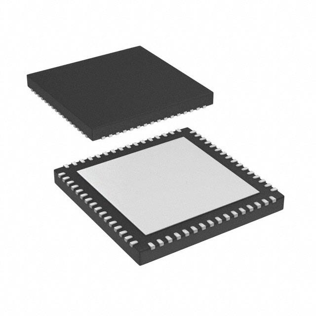


 工商网监
湘ICP备2023018690号
工商网监
湘ICP备2023018690号
