Product
Folder
Order
Now
Technical
Documents
Support &
Community
Tools &
Software
ADS7056
SBAS769 – MARCH 2017
ADS7056 Ultra-Low Power, Ultra-Small Size, 14-Bit, High-Speed SAR ADC
1 Features
3 Description
•
•
The ADS7056 is a 14-bit, 2.5-MSPS, analog-to-digital
converter (ADC). The device includes a capacitorbased, successive-approximation register (SAR) ADC
that supports a wide analog input voltage range (0 V
to AVDD, for AVDD in the range of 2.35 V to 3.6 V).
1
•
•
•
•
•
•
•
2.5-MSPS Throughput
Ultra-Small Size SAR ADC:
– X2QFN-8 Package with 2.25-mm2 Footprint
Wide Operating Range:
– AVDD: 2.35 V to 3.6 V
– DVDD: 1.65 V to 3.6 V (Independent of AVDD)
– Temperature Range: –40°C to +125°C
Unipolar Input Range: 0 V to AVDD
Excellent Performance:
– 14-Bit NMC DNL, ±2-LSB INL
– 74.5-dB SINAD at 2-kHz
– 73.7-dB SINAD at 1-MHz
Ultra-Low Power Consumption:
– 3.5 mW at 2.5-MSPS with 3.3-V AVDD
– 158 µW at 100-kSPS with 3.3-V AVDD
Integrated Offset Calibration
SPI-Compatible Serial Interface: 60-MHz
JESD8-7A Compliant Digital I/O
The SPI-compatible serial interface is controlled by
the CS and SCLK signals. The input signal is
sampled with the CS falling edge and SCLK is used
for conversion and serial data output. The device
supports a wide digital supply range (1.65 V to 3.6 V),
enabling direct interfacing to a variety of host
controllers. The ADS7056 complies with the JESD87A standard for a normal DVDD range (1.65 V to
1.95 V).
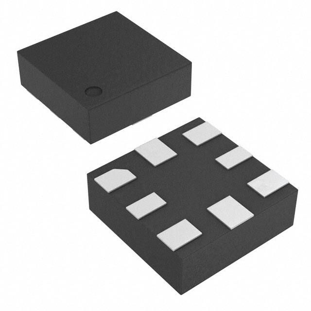
The ADS7056 is available in an 8-pin, miniature,
X2QFN package and is specified over the extended
industrial temperature range (–40°C to +125°C).
Miniature form-factor and extremely low-power
consumption make this device suitable for spaceconstrained and battery-powered applications.
Device Information(1)
PART NAME
PACKAGE
BODY SIZE (NOM)
X2QFN (8)
1.50 mm × 1.50 mm
2 Applications
ADS7056
•
•
•
•
•
•
•
•
(1) For all available packages, see the orderable addendum at
the end of the datasheet.
Sonar Receivers
Optical Line Cards and Modules
Thermal Imaging
Ultrasonic Flow Meters
Motor Controls
Handheld Radios
Environmental Sensing
Fire and Smoke Detection
Typical Application
SONAR TX
AVDD
AVDD used as Reference for
device
+
OPA836
R
AVDD
AINP
Device
SONAR RX
C
AINM
GND
RUG (8)
Actual Device Size
1.5 x 1.5 x 0.35(H) mm
1.
5m
m
mm
1.5
NOTE: The ADS7056 is smaller than a 0805 (2012
metric) SMD component.
1
An IMPORTANT NOTICE at the end of this data sheet addresses availability, warranty, changes, use in safety-critical applications,
intellectual property matters and other important disclaimers. PRODUCTION DATA.
�ADS7056
SBAS769 – MARCH 2017
www.ti.com
Table of Contents
1
2
3
4
5
6
Features ..................................................................
Applications ...........................................................
Description .............................................................
Revision History.....................................................
Pin Configuration and Functions .........................
Specifications.........................................................
1
1
1
2
3
3
6.1
6.2
6.3
6.4
6.5
6.6
6.7
6.8
3
3
4
4
4
6
6
8
Absolute Maximum Ratings .....................................
ESD Ratings..............................................................
Recommended Operating Conditions.......................
Thermal Information ..................................................
Electrical Characteristics...........................................
Timing Requirements ................................................
Switching Characteristics ..........................................
Typical Characteristics ..............................................
7
Parameter Measurement Information ................ 14
8
Detailed Description ............................................ 15
8.3 Feature Description................................................. 16
8.4 Device Functional Modes........................................ 19
9
Application and Implementation ........................ 23
9.1 Application Information............................................ 23
9.2 Typical Applications ................................................ 23
10 Power Supply Recommendations ..................... 30
10.1 AVDD and DVDD Supply Recommendations....... 30
10.2 Optimizing Power Consumed by the Device ........ 30
11 Layout................................................................... 31
11.1 Layout Guidelines ................................................. 31
11.2 Layout Example .................................................... 31
12 Device and Documentation Support ................. 32
12.1
12.2
12.3
12.4
12.5
12.6
7.1 Digital Voltage Levels ............................................. 14
8.1 Overview ................................................................. 15
8.2 Functional Block Diagram ....................................... 15
Documentation Support ........................................
Receiving Notification of Documentation Updates
Community Resources..........................................
Trademarks ...........................................................
Electrostatic Discharge Caution ............................
Glossary ................................................................
32
32
32
32
32
32
13 Mechanical, Packaging, and Orderable
Information ........................................................... 32
4 Revision History
2
DATE
REVISION
NOTES
March 2017
*
Initial release.
Submit Documentation Feedback
Copyright © 2017, Texas Instruments Incorporated
Product Folder Links: ADS7056
�ADS7056
www.ti.com
SBAS769 – MARCH 2017
5 Pin Configuration and Functions
8
AINM
RUG Package
8-Pin X2QFN
Top View
1
7
AINP
SDO
2
6
AVDD
SCLK
3
5
GND
4
CS
DVDD
Not to scale
Pin Functions
PIN
NO.
I/O
AINM
NAME
8
Analog input
Analog signal input, negative
DESCRIPTION
AINP
7
Analog input
Analog signal input, positive
AVDD
6
Supply
CS
1
Digital input
DVDD
4
Supply
Digital I/O supply voltage
GND
5
Supply
Ground for power supply, all analog and digital signals are referred to this pin
SCLK
3
Digital input
SDO
2
Digital output
Analog power-supply input, also provides the reference voltage to the ADC
Chip-select signal, active low
Serial clock
Serial data out
6 Specifications
6.1 Absolute Maximum Ratings (1)
MIN
MAX
UNIT
AVDD to GND
–0.3
3.9
V
DVDD to GND
–0.3
3.9
V
AINP to GND
–0.3
AVDD + 0.3
V
AINM to GND
–0.3
0.3
V
mA
Input current to any pin except supply pins
–10
10
Digital input voltage to GND
–0.3
DVDD + 0.3
V
Storage temperature, Tstg
–60
150
°C
(1)
Stresses beyond those listed under Absolute Maximum Ratings may cause permanent damage to the device. These are stress ratings
only, which do not imply functional operation of the device at these or any other conditions beyond those indicated under Recommended
Operating Conditions. Exposure to absolute-maximum-rated conditions for extended periods may affect device reliability.
6.2 ESD Ratings
VALUE
V(ESD)
(1)
(2)
Electrostatic discharge
Human body model (HBM), per ANSI/ESDA/JEDEC JS-001 (1)
±2000
Charged device model (CDM), per JEDEC specification JESD22-C101 (2)
±1000
UNIT
V
JEDEC document JEP155 states that 500-V HBM allows safe manufacturing with a standard ESD control process.
JEDEC document JEP157 states that 250-V CDM allows safe manufacturing with a standard ESD control process.
Submit Documentation Feedback
Copyright © 2017, Texas Instruments Incorporated
Product Folder Links: ADS7056
3
�ADS7056
SBAS769 – MARCH 2017
www.ti.com
6.3 Recommended Operating Conditions
over operating free-air temperature range (unless otherwise noted)
MIN
NOM
MAX
UNIT
AVDD
Analog supply voltage range
2.35
3
3.6
DVDD
Digital supply voltage range
1.65
1.8
3.6
V
V
TA
Operating free-air temperature
–40
25
125
°C
6.4 Thermal Information
ADS7056
THERMAL METRIC (1)
RUG (X2QFN)
UNIT
8 PINS
RθJA
Junction-to-ambient thermal resistance
177.5
°C/W
RθJC(top)
Junction-to-case (top) thermal resistance
51.5
°C/W
RθJB
Junction-to-board thermal resistance
76.7
°C/W
ψJT
Junction-to-top characterization parameter
1
°C/W
ψJB
Junction-to-board characterization parameter
76.7
°C/W
RθJC(bot)
Junction-to-case (bottom) thermal resistance
N/A
°C/W
(1)
For more information about traditional and new thermal metrics, see the Semiconductor and IC Package Thermal Metrics application
report.
6.5 Electrical Characteristics
at AVDD = 3.3 V, DVDD = 1.65 V to 3.6 V, fSAMPLE = 2.5 MSPS, and VAINM = 0 V (unless otherwise noted); minimum and
maximum values for TA = –40°C to +125°C; typical values at TA = 25°C
PARAMETER
TEST CONDITIONS
MIN
TYP
MAX
UNIT
V
ANALOG INPUT
Full-scale input voltage span (1)
Absolute input
voltage range
CS
0
AVDD
AINP to GND
–0.1
AVDD + 0.1
AINM to GND
–0.1
0.1
Sampling capacitance
V
16
pF
14
Bits
SYSTEM PERFORMANCE
Resolution
NMC
No missing codes
14
INL (2)
Integral nonlinearity
–3
±2
3
LSB (3)
DNL
Differential nonlinearity
–0.99
±0.5
1
LSB
–6
±2.5
6
EO
(2)
Offset error
dVOS/dT
Offset error drift with temperature
EG (2)
Gain error
After calibration (4)
Bits
1.75
–0.1
±0.01
Gain error drift with temperature
LSB
ppm/°C
0.1
0.5
%FS
ppm/°C
SAMPLING DYNAMICS
tCONV
Conversion time
tACQ
Acquisition time
fSAMPLE
Maximum throughput rate
18 × tSCLK
2.5
Aperture jitter, RMS
4
ns
60-MHz SCLK, AVDD = 2.35 V to 3.6 V
Aperture delay
(1)
(2)
(3)
(4)
ns
95
MHz
3
ns
12
ps
Ideal input span; does not include gain or offset error.
See Figure 32, Figure 33, and Figure 34 for statistical distribution data for INL, offset error, and gain error.
LSB means least significant bit.
See the OFFCAL State section for details.
Submit Documentation Feedback
Copyright © 2017, Texas Instruments Incorporated
Product Folder Links: ADS7056
�ADS7056
www.ti.com
SBAS769 – MARCH 2017
Electrical Characteristics (continued)
at AVDD = 3.3 V, DVDD = 1.65 V to 3.6 V, fSAMPLE = 2.5 MSPS, and VAINM = 0 V (unless otherwise noted); minimum and
maximum values for TA = –40°C to +125°C; typical values at TA = 25°C
PARAMETER
TEST CONDITIONS
MIN
TYP
72
74.9
MAX
UNIT
DYNAMIC CHARACTERISTICS
AVDD = 3.3 V
SNR
Signal-to-noise ratio (5)
THD
Total harmonic distortion (5) (6)
AVDD = 2.5 V
fIN = 2 kHz
SFDR
BW(fp)
Signal-to-noise and distortion (5)
Spurious-free dynamic range (5)
Full-power bandwidth
–85
fIN = 250 kHz
–84.8
fIN = 1000 kHz
–84.5
fIN = 2 kHz
SINAD
dB
73.7
71.75
74.5
fIN = 250 kHz
73.7
fIN = 1000 kHz
73.7
fIN = 2 kHz
89.8
fIN = 250 kHz
dB
dB
88
fIN = 1000 kHz
87.5
At –3 dB
200
dB
MHz
DIGITAL INPUT/OUTPUT (CMOS Logic Family)
VIH
High-level input voltage (7)
0.65 DVDD
DVDD + 0.3
V
VIL
Low-level input voltage (7)
–0.3
0.35 DVDD
V
0.8 DVDD
DVDD
At Isource = 2 mA
DVDD – 0.45
DVDD
At Isink = 500 µA
0
0.2 DVDD
At Isink = 2 mA
0
0.45
(7)
VOH
High-level output voltage
VOL
Low-level output voltage (7)
At Isource = 500 µA
V
V
POWER-SUPPLY REQUIREMENTS
AVDD
Analog supply voltage
2.35
3
3.6
V
DVDD
Digital I/O supply voltage
1.65
3
3.6
V
AVDD = 3.3 V, fSAMPLE = 2.5 MSPS
1050
1250
AVDD = 3.3 V, fSAMPLE = 100 kSPS
48
50
AVDD = 3.3 V, fSAMPLE = 10 kSPS
5
IAVDD
IDVDD
(5)
(6)
(7)
(8)
Analog supply current
Digital supply current
AVDD = 2.5 V, fSAMPLE = 2.5 MSPS
750
Static current with CS and SCLK high
0.02
DVDD = 1.8 V, CSDO = 20 pF,
output code = 2AAAh (8)
630
DVDD = 1.8 V, static current with CS
and SCLK high
0.01
µA
µA
All specifications expressed in decibels (dB) refer to the full-scale input (FSR) and are tested with an input signal 0.5 dB below full-scale,
unless otherwise noted.
Calculated on the first nine harmonics of the input frequency.
Digital voltage levels comply with the JESD8-7A standard for DVDD from 1.65 V to 1.95 V; see the Parameter Measurement Information
section for details.
See the Estimating Digital Power Consumption section for details.
Submit Documentation Feedback
Copyright © 2017, Texas Instruments Incorporated
Product Folder Links: ADS7056
5
�ADS7056
SBAS769 – MARCH 2017
www.ti.com
6.6 Timing Requirements
all specifications are at AVDD = 2.35 V to 3.6 V, DVDD = 1.65 V to 3.6 V, and CLOAD-SDO = 20 pF (unless otherwise noted);
minimum and maximum values for TA = –40°C to +125°C; typical values at TA = 25°C
MIN
TYP
MAX
UNIT
tCLK
Time period of SCLK
16.66
ns
tsu_CSCK
tht_CKCS
Setup time: CS falling edge to SCLK falling edge
7
ns
Hold time: SCLK rising edge to CS rising edge
8
tph_CK
SCLK high time
0.45
0.55
tSCLK
tpl_CK
SCLK low time
0.45
0.55
tSCLK
tph_CS
CS high time
ns
15
ns
6.7 Switching Characteristics
all specifications are at AVDD = 2.35 V to 3.6 V, DVDD = 1.65 V to 3.6 V, and CLOAD-SDO = 20 pF (unless otherwise noted);
minimum and maximum values for TA = –40°C to +125°C; typical values at TA = 25°C
PARAMETER
TEST CONDITIONS
MIN
TYP
MAX
UNIT
tCYCLE (1)
Cycle time
tCONV
Conversion time
tden_CSDO
Delay time: CS falling edge to data enable
6.5
ns
td_CKDO
Delay time: SCLK rising edge to (next) data
valid on SDO
10
ns
tht_CKDO
SCLK rising edge to current data invalid
2.5
tdz_CSDO
Delay time: CS rising edge to SDO going to
tri-state
5.5
(1)
400
ns
18 × tSCLK
ns
ns
tCYCLE = 1 / fSAMPLE.
Sample
A+1
Sample
A
tph_CS
tCYCLE
tACQ
tCONV
CS
SCLK
SDO
1
2
0
15
3
D13
16
D0
D12
17
0
0
18
0
Data Output for Sample A-1
Figure 1. Serial Transfer Frame
6
Submit Documentation Feedback
Copyright © 2017, Texas Instruments Incorporated
Product Folder Links: ADS7056
�ADS7056
www.ti.com
SBAS769 – MARCH 2017
tCLK
tph_CK
CS
50%
tsu_CSCK
SCLK
SCLK
50%
td_CKDO
tht_CKCS
50%
tpl_CK
50%
SDO
tht_CKDO
tden_CSDO
tdz_CSDO
SDO
Figure 2. Timing Specifications
Submit Documentation Feedback
Copyright © 2017, Texas Instruments Incorporated
Product Folder Links: ADS7056
7
�ADS7056
SBAS769 – MARCH 2017
www.ti.com
6.8 Typical Characteristics
0
0
-30
-30
-60
-60
Amplitude (dB)
Amplitude (dB)
at TA = 25°C, AVDD = 3.3 V, DVDD = 1.8 V, fIN = 2 kHz, and fSample = 2.5 MSPS (unless otherwise noted)
-90
-120
-90
-120
-150
-150
-180
-180
0
250
500
750
Frequency (kHz)
1000
0
1250
250
D001
SNR = 75.2 dB, THD = –90.25 dB, ENOB = 12.18 bits
1000
D002
Figure 4. Typical FFT
0
-30
-30
-60
-60
Amplitude (dB)
0
-90
-120
-150
-90
-120
-150
-180
-180
0
250
500
750
Frequency (kHz)
1000
1250
0
250
D003
SNR = 74.2 dB, THD = –90.25 dB, fIN = 500 kHz
500
750
Frequency (kHz)
1000
Figure 5. Typical FFT
D004
Figure 6. Typical FFT
76
SNR
SINAD
SNR
SINAD
75
SNR, SINAD (dB)
SNR, SINAD (dB)
75
74
74
73
73
72
-40
1250
SNR = 73.9 dB, THD = –87.1 dB, fIN = 1000 kHz
76
72
-7
26
59
Free-Air Temperature (qC)
92
125
0
250
D005
Figure 7. SNR and SINAD vs Temperature
8
1250
SNR = 74.3 dB, THD = –87.9 dB, fIN = 250 kHz
Figure 3. Typical FFT
Amplitude (dB)
500
750
Frequency (kHz)
500
Input Frequency (kHz)
750
1000
D006
Figure 8. SNR and SINAD vs Input Frequency
Submit Documentation Feedback
Copyright © 2017, Texas Instruments Incorporated
Product Folder Links: ADS7056
�ADS7056
www.ti.com
SBAS769 – MARCH 2017
Typical Characteristics (continued)
at TA = 25°C, AVDD = 3.3 V, DVDD = 1.8 V, fIN = 2 kHz, and fSample = 2.5 MSPS (unless otherwise noted)
76
Total Harmonic Distortion (dB)
-80
SNR, SINAD (dB)
75
74
73
-82
-84
-86
-88
SNR
SINAD
72
2.35
2.6
2.85
3.1
Reference Voltage (V)
3.35
-90
-40
3.6
-7
Figure 9. SNR and SINAD vs Reference Voltage (AVDD)
125
D008
Figure 10. THD vs Temperature
Total Harmonic Distortion (dB)
Spurious-Free Dynamic Range (dB)
92
-80
95
93
91
89
87
85
-40
-82
-84
-86
-88
-90
-92
-7
26
59
Free-Air Temperature (qC)
92
0
125
250
D009
Figure 11. SFDR vs Temperature
500
750
Input Frequency (kHz)
1000
D010
Figure 12. THD vs Input Frequency
97
-80
95
Total Harmonic Distortion (dB)
Spurious-Free Dynamic Range (dB)
26
59
Free-Air Temperature (qC)
D007
93
91
89
87
85
0
250
500
750
Input Frequency (kHz)
1000
-82
-84
-86
-88
-90
2.35
2.6
D011
Figure 13. SFDR vs Input Frequency
2.85
3.1
Reference Voltage (V)
3.35
3.6
D012
Figure 14. THD vs Reference Voltage (AVDD)
Submit Documentation Feedback
Copyright © 2017, Texas Instruments Incorporated
Product Folder Links: ADS7056
9
�ADS7056
SBAS769 – MARCH 2017
www.ti.com
Typical Characteristics (continued)
at TA = 25°C, AVDD = 3.3 V, DVDD = 1.8 V, fIN = 2 kHz, and fSample = 2.5 MSPS (unless otherwise noted)
30000
95
Spurious-Free Dynamic Range (dB)
27000
24000
93
21000
Number of Hits
91
89
18000
15000
12000
9000
6000
87
3000
85
2.35
0
2.6
2.85
3.1
Reference Voltage (V)
3.35
8188 8189 8190 8191 8192 8193 8194 8195 8196
Code
D014
3.6
D013
Standard deviation of codes = 0.94 LSB, VIN = AVDD / 2
Figure 15. SFDR vs Reference Voltage (AVDD)
Figure 16. DC Input Histogram
2
2
Calibrated
Uncalibrated
Calibrated
Uncalibrated
1
Offset (LSB)
Offset (LSB)
1
0
-1
0
-1
-2
-40
-7
26
59
Free-Air Temperature (qC)
92
-2
2.35
125
2.6
D015
Figure 17. Offset vs Temperature
2.85
3.1
Reference Voltage (V)
3.35
3.6
D016
Figure 18. Offset vs Reference Voltage (AVDD)
1
0.1
Differential Nonlinearity (LSB)
Calibrated
Uncalibrated
Gain Error (%FS)
0.05
0
-0.05
-0.1
-40
0.5
0
-0.5
-1
-7
26
59
Free-Air Temperature (qC)
92
125
0
D017
Figure 19. Gain Error vs Temperature
10
Submit Documentation Feedback
3300
6600
9900
Code
13200
16500
D019
Figure 20. Typical DNL
Copyright © 2017, Texas Instruments Incorporated
Product Folder Links: ADS7056
�ADS7056
www.ti.com
SBAS769 – MARCH 2017
Typical Characteristics (continued)
at TA = 25°C, AVDD = 3.3 V, DVDD = 1.8 V, fIN = 2 kHz, and fSample = 2.5 MSPS (unless otherwise noted)
1
Differential Nonlinearity (LSB)
Integral Nonlinearity (LSB)
3
1.5
0
-1.5
0.5
0
-0.5
-1
-3
0
3300
6600
9900
13200
0
16500
Code
3300
6600
9900
13200
16500
Code
D020
D021
AVDD = 2.35 V
Figure 21. Typical INL
Figure 22. Typical DNL
1
3
Differential Nonlinearity (LSB)
Integral Nonlinearity (LSB)
Minimum
Maximum
1.5
0
-1.5
3300
6600
9900
13200
16500
Code
0
-0.5
-1
-40
-3
0
0.5
-7
D022
26
59
Free-Air Temperature (qC)
92
125
D023
AVDD = 2.35 V
Figure 23. Typical INL
Figure 24. DNL vs Temperature
1
3
Minimum
Integral Nonlinearity (LSB)
Differential Nonlinearity (LSB)
Minimum
Maximum
0.5
0
-0.5
-1
2.35
2.6
2.85
3.1
Reference Voltage (V)
3.35
3.6
Maximum
1.5
0
-1.5
-3
-40
D024
Figure 25. DNL vs Reference Voltage
-7
26
59
Free-Air Temperature (qC)
92
Product Folder Links: ADS7056
D025
Figure 26. INL vs Temperature
Submit Documentation Feedback
Copyright © 2017, Texas Instruments Incorporated
125
11
�ADS7056
SBAS769 – MARCH 2017
www.ti.com
Typical Characteristics (continued)
at TA = 25°C, AVDD = 3.3 V, DVDD = 1.8 V, fIN = 2 kHz, and fSample = 2.5 MSPS (unless otherwise noted)
1.11
3
Maximum
1.095
1.5
Supply Current (mA)
0
-1.5
1.08
1.065
1.05
-3
2.35
2.6
2.85
3.1
Reference Voltage (V)
3.35
1.035
-40
3.6
-7
92
125
D027
Figure 28. AVDD Current vs Temperature
1200
1200
960
1080
Supply Current (µA)
720
480
240
960
840
720
0
600
2.35
2500
Figure 29. AVDD Current vs Throughput
600
300
92
3.6
D029
125
3500
3250
3000
2750
2500
2250
2000
1750
1500
1250
1000
750
500
250
0
D030
3
900
26
59
Free-Air Temperature (qC)
3.35
2
2.
5
Frequency
1200
-7
2.85
3.1
Supply Voltage (V)
Figure 30. AVDD Current vs AVDD Voltage
1500
0
-40
2.6
D028
1
1.
5
2000
0
0.
5
1000
1500
Throughput (Ksps)
0
500
-1
-0
.5
0
-3
-2
.5
Supply Current (µA)
Figure 27. INL vs Reference Voltage
IAVDD Static (nA)
26
59
Free-Air Temperature (qC)
D026
-2
-1
.5
Integral Nonlinearity (LSB)
Minimum
6000 Devices
CS = DVDD
Figure 31. Static AVDD Current vs Temperature
12
Submit Documentation Feedback
Figure 32. Typical INL Distribution
Copyright © 2017, Texas Instruments Incorporated
Product Folder Links: ADS7056
�ADS7056
www.ti.com
SBAS769 – MARCH 2017
Typical Characteristics (continued)
at TA = 25°C, AVDD = 3.3 V, DVDD = 1.8 V, fIN = 2 kHz, and fSample = 2.5 MSPS (unless otherwise noted)
1200
4500
4000
1000
3500
3000
Frequency
Frequency
800
600
400
2500
2000
1500
1000
200
500
0
0.
05
0.
04
0.
03
0
1
0.
02
0.
0
.0
1
-0
.0
2
.0
3
-0
.0
4
-0
.0
5
-0
-0
6000 Devices
6
5
5
5.
4
5
4.
3
5
3.
2
2.
5
1
5
1.
0
5
0.
-2
.5
-2
-1
.5
-1
-0
.5
0
6000 Devices
Figure 33. Typical Offset Error Distribution
Figure 34. Typical Gain Error Distribution
Submit Documentation Feedback
Copyright © 2017, Texas Instruments Incorporated
Product Folder Links: ADS7056
13
�ADS7056
SBAS769 – MARCH 2017
www.ti.com
7 Parameter Measurement Information
7.1 Digital Voltage Levels
The device complies with the JESD8-7A standard for DVDD from 1.65 V to 1.95 V. Figure 35 shows voltage
levels for the digital input and output pins.
Digital Output
DVDD
VOH
DVDD-0.45V
SDO
0.45V
VOL
0V
ISource= 2 mA, ISink = 2 mA,
DVDD = 1.65 V to 1.95 V
Digital Inputs
DVDD + 0.3V
VIH
0.65DVDD
CS
SCLK
0.35DVDD
-0.3V
VIL
DVDD = 1.65 V to 1.95 V
Figure 35. Digital Voltage Levels as per the JESD8-7A Standard
14
Submit Documentation Feedback
Copyright © 2017, Texas Instruments Incorporated
Product Folder Links: ADS7056
�ADS7056
www.ti.com
SBAS769 – MARCH 2017
8 Detailed Description
8.1 Overview
The ADS7056 is a 14-bit, 2.5-MSPS, analog-to-digital converter (ADC). The device includes a capacitor-based,
successive-approximation register (SAR) ADC that supports a wide analog input voltage range (0 V to AVDD, for
AVDD in the range of 2.35 V to 3.6 V). The device uses the AVDD supply voltage as the reference voltage for
conversion of analog input to digital output and the AVDD supply voltage also powers the analog blocks of the
device. The device has integrated offset calibration feature to calibrate its own offset; see the OFFCAL State
section for details.
The SPI-compatible serial interface is controlled by the CS and SCLK signals. The input signal is sampled with
the CS falling edge and SCLK is used for conversion and serial data output. The device supports a wide digital
supply range (1.65 V to 3.6 V), enabling direct interface to a variety of host controllers. The ADS7056 complies
with the JESD8-7A standard for a normal DVDD range (1.65 V to 1.95 V); see the Digital Voltage Levels section
for details.
The ADS7056 is available in 8-pin, miniature, X2QFN package and is specified over extended industrial
temperature range (–40°C to 125°C). Miniature form-factor and extremely low-power consumption make this
device suitable for space-constrained, battery-powered applications.
8.2 Functional Block Diagram
AVDD
DVDD
GND
Offset
Calibration
AINP
CS
CDAC
Comparator
SCLK
Serial
Interface
AINM
SDO
SAR
Submit Documentation Feedback
Copyright © 2017, Texas Instruments Incorporated
Product Folder Links: ADS7056
15
�ADS7056
SBAS769 – MARCH 2017
www.ti.com
8.3 Feature Description
8.3.1 Analog Input
The device supports a unipolar, single-ended analog input signal. Figure 36 shows a small-signal equivalent
circuit of the sample-and-hold circuit. The sampling switch is represented by a resistance (RS1 and RS2, typically
50 Ω) in series with an ideal switch (SW1 and SW2). The sampling capacitors, CS1 and CS2, are typically 16 pF.
AVDD
SW1
Rs1
AINP
Cs1
GND
V_BIAS
AVDD
Cs2
SW2
Rs2
AINM
GND
Figure 36. Equivalent Input Circuit for the Sampling Stage
During the acquisition process, both positive and negative inputs are individually sampled on CS1 and CS2,
respectively. During the conversion process, the device converts for the voltage difference between the two
sampled values: VAINP – VAINM.
Each analog input pin has electrostatic discharge (ESD) protection diodes to AVDD and GND. Keep the analog
inputs within the specified range to avoid turning the diodes on.
The full-scale analog input range (FSR) is 0 V to AVDD and the absolute input range on the AINM and AINP pins
is –0.1 V to AVDD + 0.1 V.
16
Submit Documentation Feedback
Copyright © 2017, Texas Instruments Incorporated
Product Folder Links: ADS7056
�ADS7056
www.ti.com
SBAS769 – MARCH 2017
Feature Description (continued)
8.3.2 Reference
The device uses the analog supply voltage (AVDD) as the reference voltage for the analog-to-digital conversion.
During the conversion process, the internal capacitors are switched to the AVDD pin as per the successive
approximation algorithm. As shown in Figure 37, a 3.3-µF (CAVDD), low equivalent series resistance (ESR)
ceramic capacitor is recommended to be placed between the AVDD and GND pins. The decoupling capacitor
provides the instantaneous charge required by the internal circuit during the conversion process and maintains a
stable dc voltage on the AVDD pin.
See the Power Supply Recommendations and Layout Example sections for component recommendations and
layout guidelines.
AVDD
CAVDD
GND
CDVDD
DVDD
Figure 37. Reference for the Device
Submit Documentation Feedback
Copyright © 2017, Texas Instruments Incorporated
Product Folder Links: ADS7056
17
�ADS7056
SBAS769 – MARCH 2017
www.ti.com
Feature Description (continued)
8.3.3 ADC Transfer Function
The device supports a unipolar, single-ended analog input signal. The output is in straight binary format.
Figure 38 and Table 1 show the ideal transfer characteristics for the device.
The least significant bit for the device is given by:
1 LSB = VREF / 2N
where:
•
•
VREF = Voltage applied between the AVDD and GND pins and
N = 14
(1)
ADC Code (Hex)
PFSC
MC + 1
MC
NFSC+1
NFSC
VREF
2
1 LSB
VIN
V REF
2
VREF ± 1 LSB
1LSB
Single-Ended Analog Input
(AINP ± AINM)
Figure 38. Ideal Transfer Characteristics
Table 1. Transfer Characteristics
INPUT VOLTAGE (AINP – AINM)
18
CODE
DESCRIPTION
IDEAL OUTPUT CODE
(Hex)
0000
≤ 1 LSB
NFSC
Negative full-scale code
1 LSB to 2 LSBs
NFSC + 1
—
0001
VREF / 2 to VREF / 2 + 1 LSB
MC
Mid code
1FFF
VREF / 2 + 1 LSB to VREF / 2 + 2 LSBs
MC + 1
—
2000
≥ VREF – 1 LSB
PFSC
Positive full-scale code
3FFF
Submit Documentation Feedback
Copyright © 2017, Texas Instruments Incorporated
Product Folder Links: ADS7056
�ADS7056
www.ti.com
SBAS769 – MARCH 2017
8.4 Device Functional Modes
The device supports a simple, SPI-compatible interface to the external host. On power-up, the device is in ACQ
state. The CS signal defines one conversion and serial data transfer frame. A frame starts with a CS falling edge
and ends with a CS rising edge. The SDO pin is tri-stated when CS is high. With CS low, the clock provided on
the SCLK pin is used for conversion and data transfer and the output data are available on the SDO pin.
As shown in Figure 39, the device supports three functional states: acquisition (ACQ), conversion (CNV), and
offset calibration (OFFCAL). The device status depends on the CS and SCLK signals provided by the host
controller.
ACQ
Ca
lib
End of Conversion
OFFCAL
Falling Edge of CS
or
n
io
t
ra
lib f CS
a
p
tC eo
-U
fse Edg
er
f
w
O
Po
of ng
d isi
on
n
En R
io
at
br
i
l
Ca
ra
tio
Op n du
e r ri n
at g
io N
n
or
m
al
CONV
Figure 39. Functional State Diagram
8.4.1 ACQ State
In ACQ state, switches SW1 and SW2 connected to the analog input pins close and the device acquires the
analog input signal on CS1 and CS2. The device enters ACQ state at power-up, at the end of every conversion,
and after completing the offset calibration. A CS falling edge takes the device from ACQ state to CNV state.
The device consumes extremely low power from the AVDD and DVDD power supplies when in ACQ state.
Submit Documentation Feedback
Copyright © 2017, Texas Instruments Incorporated
Product Folder Links: ADS7056
19
�ADS7056
SBAS769 – MARCH 2017
www.ti.com
Device Functional Modes (continued)
8.4.2 CNV State
In the CNV state, the device uses the external clock to convert the sampled analog input signal to an equivalent
digital code as per the transfer function illustrated in Figure 38. The conversion process requires a minimum of
18 SCLK falling edges to be provided within the frame. After the end of conversion process, the device
automatically moves from CNV state to ACQ state. For acquisition of the next sample, a minimum time of tACQ
must be provided.
Figure 40 shows a detailed timing diagram for the serial interface. In the first serial transfer frame after power-up,
the device provides the first data as all zeros. In any frame, the clocks provided on the SCLK pin are also used to
transfer the output data for the previous conversion. A leading 0 is output on the SDO pin on the CS falling edge.
The most significant bit (MSB) of the output data is launched on the SDO pin on the rising edge after the first
SCLK falling edge. Subsequent output bits are launched on the subsequent rising edges provided on SCLK.
When all 14 output bits are shifted out, the device outputs 0's on the subsequent SCLK rising edges. The device
enters ACQ state after 18 clocks and a minimum time of tACQ must be provided for acquiring the next sample. If
the device is provided with less than 18 SCLK falling edges in the present serial transfer frame, the device
provides an invalid conversion result in the next serial transfer frame.
Sample
A+1
Sample
A
tph_CS
tCYCLE
tACQ
tCONV
CS
SCLK
SDO
1
2
0
15
3
D13
16
D0
D12
17
0
18
0
0
Data Output for Sample A-1
Figure 40. Serial Interface Timing Diagram
8.4.3 OFFCAL State
In OFFCAL state, the device calibrates and corrects for its internal offset errors. In OFFCAL state, the sampling
capacitors are disconnected from the analog input pins (AINP and AINM). The offset calibration is effective for all
subsequent conversions until the device is powered off. An offset calibration cycle is recommended at power-up
and whenever there is a significant change in the operating conditions for the device (such as in the AVDD
voltage and operating temperature).
The host controller must provide a serial transfer frame as described in Figure 41 or in Figure 42 to enter
OFFCAL state.
20
Submit Documentation Feedback
Copyright © 2017, Texas Instruments Incorporated
Product Folder Links: ADS7056
�ADS7056
www.ti.com
SBAS769 – MARCH 2017
Device Functional Modes (continued)
8.4.3.1 Offset Calibration on Power-Up
On power-up, the host must provide 24 SCLKs in the first serial transfer to enter the OFFCAL state. The device
provides 0's on SDO during offset calibration. For acquisition of the next sample, a minimum time of tACQ must be
provided. If the host controller enters the OFFCAL state, but pulls the CS pin high before providing 24 SCLKs,
then the offset calibration process is aborted and the device enters the ACQ state. Figure 41 and Table 2 provide
the timing for offset calibration on power-up.
First
Sample
Next
Sample
tCYCLE
tACQ
CS
SCLK
SDO
1
2
0
4
3
0
24
0
0
0
0
Data Output for First Sample
Figure 41. Timing for Offset Calibration on Power-Up
Table 2. Timing Specifications for Offset Calibration on Power-Up (1)
MIN
tcycle
Cycle time for offset calibration on power-up
tACQ
Acquisition time
fSCLK
Frequency of SCLK
(1)
TYP
MAX
UNIT
24 × tCLK + tACQ
ns
95
ns
60
MHz
In addition to the timing specifications of Figure 41 and Table 2, the timing specifications described in Figure 2 and the Timing
Requirements table are also applicable for offset calibration on power-up.
Submit Documentation Feedback
Copyright © 2017, Texas Instruments Incorporated
Product Folder Links: ADS7056
21
�ADS7056
SBAS769 – MARCH 2017
www.ti.com
8.4.3.2 Offset Calibration During Normal Operation
During normal operation, the host must provide 64 SCLKs in the serial transfer frame to enter the OFFCAL state.
The device provides the conversion result for the previous sample during the first 18 SCLKs and 0's on SDO for
the rest of the SCLKs in the serial transfer frame. For acquisition of the next sample, a minimum time of tACQ
must be provided. If the host controller enters the OFFCAL state, but pulls the CS high before providing 64
SCLKs, then the offset calibration process is aborted and the device enters ACQ state. Figure 42 and Table 3
provide the timing for offset calibration during normal operation.
Sample
A
Sample
A+1
tCYCLE
tACQ
CS
SCLK
1
SDO
2
4
3
0
D13
D12
17
16
D0
0
64
0
Data Output for Sample A-1
Figure 42. Timing for Offset Calibration During Normal Operation
Table 3. Timing Specifications for Offset Calibration During Normal Operation (1)
MIN
tcycle
Cycle time for offset calibration on power-up
tACQ
Acquisition time
fSCLK
Frequency of SCLK
(1)
22
TYP
MAX
UNIT
64 × tCLK + tACQ
ns
95
ns
60
MHz
In addition to the timing specifications of Figure 42 and Table 3, the timing specifications described in Figure 2 and the Timing
Requirements table are also applicable for offset calibration during normal operation.
Submit Documentation Feedback
Copyright © 2017, Texas Instruments Incorporated
Product Folder Links: ADS7056
�ADS7056
www.ti.com
SBAS769 – MARCH 2017
9 Application and Implementation
NOTE
Information in the following applications sections is not part of the TI component
specification, and TI does not warrant its accuracy or completeness. TI’s customers are
responsible for determining suitability of components for their purposes. Customers should
validate and test their design implementation to confirm system functionality.
9.1 Application Information
The two primary circuits required to maximize the performance of a high-precision, successive approximation
register (SAR) analog-to-digital converter (ADC) are the input driver and the reference driver circuits. This section
details some general principles for designing the input driver circuit, reference driver circuit, and provides typical
application circuits designed for the device.
9.2 Typical Applications
9.2.1 Single-Supply Data Acquisition With the ADS7056
Analog Power Supply for
ADC
REF1933
AVDD (+3.3V)
(AVDD + 0.2V) to 5.5 V
VIN
VOUT
GND
1uF
3.3uF
OPA_VDD
(+5V)
33
±
AVDD
VIN
+
+
VSOURCE
SCLK
33
33
CS
OPA836
Device
33
SDO
±
680pF
Host
Controller
GND
GND
Device: 14 Bit , 2.5 MSPS,
Single-Ended Input
Input Driver
Figure 43. DAQ Circuit: Single-Supply DAQ
9.2.1.1 Design Requirements
The goal of the circuit shown in Figure 43 is to design a single-supply data acquisition (DAQ) circuit based on the
ADS7056 with SNR greater than 74 dB and THD less than –85 dB for input frequencies of 2 kHz to 100 kHz at a
throughput of 2.5 MSPS for applications such as sonar receivers and ultrasonic flow meters.
9.2.1.2 Detailed Design Procedure
The input driver circuit for a high-precision ADC mainly consists of two parts: a driving amplifier and charge
kickback filter. Careful design of the front-end circuit is critical to meet the linearity and noise performance of a
high-precision ADC.
Submit Documentation Feedback
Copyright © 2017, Texas Instruments Incorporated
Product Folder Links: ADS7056
23
�ADS7056
SBAS769 – MARCH 2017
www.ti.com
Typical Applications (continued)
9.2.1.2.1 Low Distortion Charge Kickback Filter Design
Figure 44 shows the input circuit of a typical SAR ADC. During the acquisition phase, the SW switch closes and
connects the sampling capacitor (CSH) to the input driver circuit. This action introduces a transient on the input
pins of the SAR ADC. An ideal amplifier with 0 Ω of output impedance and infinite current drive can settle this
transient in zero time. For a real amplifier with non-zero output impedance and finite drive strength, this switched
capacitor load can create stability issues.
Charge Kickback Filter
-
VIN
RFLT
SAR ADC
SW
CSH
+
CFLT
f-3dB =
1
2 Πx RFLT x CFLT
Figure 44. Input Sample-and-Hold Circuit for a Typical SAR ADC
For ac signals, the filter bandwidth must be kept low to band-limit the noise fed into the ADC input, thereby
increasing the signal-to-noise ratio (SNR) of the system. Besides filtering the noise from the front-end drive
circuitry, the RC filter also helps attenuate the sampling charge injection from the switched-capacitor input stage
of the ADC. A filter capacitor, CFLT, is connected across the ADC inputs. This capacitor helps reduce the
sampling charge injection and provides a charge bucket to quickly charge the internal sample-and-hold
capacitors during the acquisition process. As a rule of thumb, the value of this capacitor is at least 20 times the
specified value of the ADC sampling capacitance. For this device, the input sampling capacitance is equal to
16 pF. Thus, the value of CFLT is greater than 320 pF. Select a COG- or NPO-type capacitor because these
capacitor types have a high-Q, low-temperature coefficient, and stable electrical characteristics under varying
voltages, frequency, and time.
Driving capacitive loads can degrade the phase margin of the input amplifiers, thus making the amplifier
marginally unstable. To avoid amplifier stability issues, series isolation resistors (RFLT) are used at the output of
the amplifiers. A higher value of RFLT is helpful from the amplifier stability perspective, but adds distortion as a
result of interactions with the nonlinear input impedance of the ADC. Distortion increases with source impedance,
input signal frequency, and input signal amplitude. Therefore, the selection of RFLT requires balancing the stability
and distortion of the design.
24
Submit Documentation Feedback
Copyright © 2017, Texas Instruments Incorporated
Product Folder Links: ADS7056
�ADS7056
www.ti.com
SBAS769 – MARCH 2017
Typical Applications (continued)
9.2.1.2.2 Input Amplifier Selection
Selection criteria for the input amplifiers is highly dependent on the input signal type as well as the performance
goals of the data acquisition system. Some key amplifier specifications to consider when selecting an appropriate
amplifier to drive the inputs of the ADC are:
• Small-signal bandwidth: select the small-signal bandwidth of the input amplifiers to be as high as possible
after meeting the power budget of the system. Higher bandwidth reduces the closed-loop output impedance
of the amplifier, thus allowing the amplifier to more easily drive the low cutoff frequency RC filter (see the Low
Distortion Charge Kickback Filter Design section for details.) at the inputs of the ADC. Higher bandwidth also
minimizes the harmonic distortion at higher input frequencies. Select the amplifier with the unity-gain
bandwidth (UGB) as described in Equation 2 to maintain the overall stability of the input driver circuit.
1
UGB t 4 u
2Πu 5FLT u &FLT
where:
•
•
UGB = unity-gain bandwidth
(2)
Noise: noise contribution of the front-end amplifiers must be as low as possible to prevent any degradation in
SNR performance of the system. Generally, to ensure that the noise performance of the data acquisition
system is not limited by the front-end circuit, the total noise contribution from the front-end circuit must be
kept below 20% of the input-referred noise of the ADC. As Equation 3 explains, noise from the input driver
circuit is band limited by designing a low cutoff frequency RC filter.
NG u
V 1 f _AMP_PP
6.6
2
Œ
e 2n_RMS u u f
2
3dB
1
VREF
d
u
u 10
5
2 2
SNR(dB)
20
where:
•
•
•
•
•
V1/f_AMP_PP is the peak-to-peak flicker noise in µVRMS
en_RMS is the amplifier broadband noise
f–3dB is the –3-dB bandwidth of the RC filter and
NG is the noise gain of the front-end circuit, which is equal to 1 in the buffer configuration
(3)
Distortion: both the ADC and the input driver introduce distortion in a data acquisition block. To ensure that
the distortion performance of the data acquisition system is not limited by the front-end circuit, the distortion of
the input driver must be at least 10 dB lower than the distortion of the ADC.
For the application circuit of Figure 43, the OPA836 is selected for its high bandwidth (205 MHz), low noise
(4.6 nV/√Hz), high output drive capacity (45 mA), and fast settling response (22 ns for 0.1% settling).
9.2.1.2.3 Reference Circuit
The analog supply voltage of the device is also used as a voltage reference for conversion. Decouple the AVDD
pin with a 3.3-µF, low-ESR ceramic capacitor.
Submit Documentation Feedback
Copyright © 2017, Texas Instruments Incorporated
Product Folder Links: ADS7056
25
�ADS7056
SBAS769 – MARCH 2017
www.ti.com
Typical Applications (continued)
9.2.1.3 Application Curves
0
0
-50
-50
Amplitude (dB)
Amplitude (dB)
Figure 45 and Figure 46 provide the measurement results for the circuit described in Figure 43.
-100
-150
-100
-150
-200
-200
0
250
500
750
Frequency (kHz)
1000
1250
0
250
500
750
Frequency (kHz)
D036
SNR = 75.8 dB, THD = –90.1 dB, SINAD = 75 dB
1000
1250
D037
SNR = 75 dB, THD = –88.7 dB, SINAD = 74.3 dB
Figure 45. Test Results for the ADS7056 and OPA836 for a
2-kHz Input
Figure 46. Test Results for the ADS7056 and OPA836 for a
100-kHz Input
9.2.2 High Bandwidth (1 MHz) Data Acquisition With the ADS7056
Analog Power Supply for
ADC
REF1933
AVDD(+3.3V)
(AVDD + 0.2V) to 5.5 V
VIN
VOUT
GND
1uF
3.3uF
499Ÿ
VDD(+6V)
499Ÿ
10
±
+
VSOURCE
±
VCM
(+0.825 V)
AVDD
AINP
+
THS4031
SCLK
33
CS
470pF
Device
SDO
VSS(-6V)
33
AINM
33
Host
Controller
GND
Device: 14 Bit , 2.5 MSPS,
Single-Ended Input
Figure 47. High Bandwidth DAQ Circuit
26
Submit Documentation Feedback
Copyright © 2017, Texas Instruments Incorporated
Product Folder Links: ADS7056
�ADS7056
www.ti.com
SBAS769 – MARCH 2017
Typical Applications (continued)
9.2.2.1 Design Requirements
Applications such as ultrasonic flow meters, global positioning systems (GPS), handheld radios, and motor
controls need analog-to-digital converters that are interfaced to high-frequency sensors (200 kHz to 1 MHz). The
goal of the circuit described in Figure 47 is to design a single-supply digital acquisition (DAQ) circuit based on the
ADS7056 with SNR greater than 73 dB and THD less than –85 dB for input frequencies of 200 kHz to 1 MHz at
a throughput of 2.5 MSPS.
9.2.2.2 Detailed Design Procedure
To achieve a SINAD greater than 73 dB, the operational amplifier must have high bandwidth in order to settle the
input signal within the acquisition time of the ADC. The operational amplifier must have low noise to keep the
total system noise below 20% of the input-referred noise of the ADC. For the application circuit shown in
Figure 47, the THS4031 is selected for its high bandwidth (275 MHz), low total harmonic distortion of –90 dB at
1 MHz, and ultra-low noise of 1.6 nV/√Hz. The THS4031 is powered up from dual power supply (VDD = 6 V and
VSS = –6 V).
For chip-select signals, high-frequency system SNR performance is highly dependent on jitter. Thus, selecting a
clock source with very low jitter (< 20-ps RMS) is recommended.
9.2.2.3 Application Curves
0
0
-50
-50
Amplitude(dB)
Amplitude (dB)
Figure 48 shows the FFT plot for the ADS7056 with a 500-kHz input frequency used for the circuit in Figure 47.
Figure 49 shows the FFT plot for the ADS7056 with a 1000-kHz input frequency used for the circuit in Figure 47.
-100
-100
-150
-150
-200
-200
0
250
500
750
Frequency (kHz)
1000
1250
0
D035
SNR = 74.2 dB, THD = –90.4 dB, SINAD = 73.5 dB
Figure 48. Test Results for the ADS7056 and THS4031 for
a 500-kHz Input
250
500
750
Frequency (kHz)
1000
1250
D038
SNR = 73.5 dB, THD = –87.8 dB, SINAD = 73 dB
Figure 49. Test Results for the ADS7056 and THS4031 for
a 1000-kHz Input
Submit Documentation Feedback
Copyright © 2017, Texas Instruments Incorporated
Product Folder Links: ADS7056
27
�ADS7056
SBAS769 – MARCH 2017
www.ti.com
Typical Applications (continued)
9.2.3 14-Bit, 10-kSPS DAQ Circuit Optimized for DC Sensor Measurements
AVDD
Sensor
RSOURCE
AVDD
AINP
+
TI Device
±
CFLT
AINM
GND
Copyright © 2017, Texas Instruments Incorporated
Figure 50. Interfacing the Device Directly With Sensors
In applications such as environmental sensors, gas detectors, and smoke or fire detectors where the input is very
slow moving and the sensor can be connected directly to the device operating at a lower throughput rate, a DAQ
circuit can be designed without the input driver for the ADC. This type of a use case is of particular interest for
applications in which the primary goal is to achieve the absolute lowest power, size, and cost. Typical
applications that fall into this category are low-power sensor applications (such as temperature, pressure,
humidity, gas, and chemical).
9.2.3.1 Design Requirements
For this design example, use the parameters listed in Table 4 as the input parameters.
Table 4. Design Parameters
DESIGN PARAMETER
GOAL VALUE
Throughput
10 kSPS
SNR at 100 Hz
74 dB
THD at 100 Hz
–85 dB
SINAD at 100 Hz
73 dB
ENOB
12 bits
Power
20 µW
9.2.3.2 Detailed Design Procedure
The ADS7056 can be directly interfaced with sensors at lower throughput without the need of an amplifier buffer.
The analog input source drive must be capable of driving the switched capacitor load of a SAR ADC and settling
the analog input signal within the acquisition time of the SAR ADC. However, the output impedance of the sensor
must be taken into account when interfacing a SAR ADC directly with sensors. Drive the analog input of the SAR
ADC with a low impedance source. The input signal requires more acquisition time to settle to the desired
accuracy because of the higher output impedance of the sensor. Figure 50 shows the simplified circuit for a
sensor as a voltage source with output impedance (Rsource).
The acquisition time of a SAR ADC (such as the ADS7056 ) can be increased by reducing throughput in the
following ways:
1. Reducing the SCLK frequency to reduce the throughput, or
2. Keeping the SCLK fixed at the highest permissible value (that is, 60 MHz for the device) and increasing the
CS high time.
28
Submit Documentation Feedback
Copyright © 2017, Texas Instruments Incorporated
Product Folder Links: ADS7056
�ADS7056
www.ti.com
SBAS769 – MARCH 2017
Table 5 lists the acquisition time for the above two cases for a throughput of 10 kSPS. Clearly, case 2 provides
more acquisition time for the input signal to settle.
Table 5. Acquisition Time with Different SCLK Frequencies
CONVERSION TIME
(= 18 × tSCLK)
ACQUISITION TIME
(= tcycle – tconv)
CASE
SCLK
tcycle
1
0.24 MHz
100 µs
75 µs
25 µs
2
60 MHz
100 µs
0.3 µs
99.7 µs
9.2.3.3 Application Curve
When the output impedance of the sensor increases, the time required for the input signal to settle increases and
the performance of the SAR ADC starts degrading if the input signal does not settle within the acquisition time of
the ADC. The performance of the SAR ADC can be improved by reducing the throughput to provide enough time
for the input signal to settle. Figure 51 provides the results for ENOB achieved from the ADS7056 for case 2 at
different throughputs with different input impedances at the device input.
12.5
ENOB (Bits)
12
11.5
11
10.5
33Ohm, 680pF
330Ohm, 680pF
3.3kOhm, 680pF
10kOhm, 680pF
20kOhm, 680pF
10
9.5
2
22
42
62
Sampling Speed(kSPS)
82
100
D039
Figure 51. Effective Number of Bits (ENOB) Achieved From the ADS7056 at Different Throughputs
Table 6 shows the results and performance summary for this 14-bit, 10-kSPS DAQ circuit application.
Table 6. Results and Performance Summary for a 14-Bit, 10-kSPS DAQ Circuit for DC Sensor
Measurements
DESIGN PARAMETER
GOAL VALUE
ACHIEVED RESULT
Throughput
10 kSPS
10 kSPS
SNR at 100 Hz
74 dB
75 dB
THD at 100 Hz
–85 dB
–89 dB
SINAD at 100 Hz
73 dB
74.3 dB
ENOB
12
12.05
Power
20 µW
17 µW
Submit Documentation Feedback
Copyright © 2017, Texas Instruments Incorporated
Product Folder Links: ADS7056
29
�ADS7056
SBAS769 – MARCH 2017
www.ti.com
10 Power Supply Recommendations
10.1 AVDD and DVDD Supply Recommendations
The device has two separate power supplies: AVDD and DVDD. AVDD powers the analog blocks and is also
used as the reference voltage for the analog-to-digital conversion. Always set the AVDD supply to be greater
than or equal to the maximum input signal to avoid saturation of codes. Decouple the AVDD pin to the GND pin
with a 3.3-µF ceramic decoupling capacitor.
DVDD is used for the interface circuits. Decouple the DVDD pin to the GND pin with a 1-µF ceramic decoupling
capacitor. Figure 52 shows the decoupling recommendations.
AVDD
CAVDD
GND
CDVDD
DVDD
Figure 52. Power-Supply Decoupling
10.2 Optimizing Power Consumed by the Device
•
•
•
•
Keep the analog supply voltage (AVDD) in the specified operating range and equal to the maximum analog
input voltage.
Keep the digital supply voltage (DVDD) in the specified operating range and at the lowest value supported by
the host controller.
Reduce the load capacitance on the SDO output.
Run the device at the optimum throughput. Power consumption reduces proportionally with the throughput.
10.2.1 Estimating Digital Power Consumption
The current consumption from the DVDD supply depends on the DVDD voltage, the load capacitance on the
SDO pin (CLOAD-SDO), and the output code, and can be calculated as:
IDVDD = CLOAD-SDO × V × f
where:
•
•
•
CLOAD-SDO = Load capacitance on the SDO pin
V = DVDD supply voltage
f = frequency of transitions on the SDO output
(4)
The number of transitions on the SDO output depends on the output code, and thus changes with the analog
input. The maximum value of f occurs when data output on the SDO change on every SCLK (that is, for output
codes of 2AAAh or 1555h). With an output code of 2AAAh, f = 17.5 MHz and when CLOAD-SDO = 20 pF and DVDD
= 1.8 V, IDVDD= 630 µA.
30
Submit Documentation Feedback
Copyright © 2017, Texas Instruments Incorporated
Product Folder Links: ADS7056
�ADS7056
www.ti.com
SBAS769 – MARCH 2017
11 Layout
11.1 Layout Guidelines
Figure 53 shows a board layout example for the device. The key considerations for layout are:
• Use a solid ground plane underneath the device and partition the PCB into analog and digital sections
• Avoid crossing digital lines with the analog signal path and keep the analog input signals and the reference
input signals away from noise sources.
• The power sources to the device must be clean and well-bypassed. Use CAVDD decoupling capacitors in close
proximity to the analog (AVDD) power supply pin.
• Use a CDVDD decoupling capacitor close to the digital (DVDD) power-supply pin.
• Avoid placing vias between the AVDD and DVDD pins and the bypass capacitors.
• Connect the ground pin to the ground plane using a short, low-impedance path.
• Place the charge kickback filter components close to the device.
Among ceramic surface-mount capacitors, COG (NPO) ceramic capacitors are recommended because these
components provide the most stable electrical properties over voltage, frequency, and temperature changes.
11.2 Layout Example
Figure 53. Example Layout
Submit Documentation Feedback
Copyright © 2017, Texas Instruments Incorporated
Product Folder Links: ADS7056
31
�ADS7056
SBAS769 – MARCH 2017
www.ti.com
12 Device and Documentation Support
12.1 Documentation Support
12.1.1 Related Documentation
For related documentation see the following:
• OPAx836 Very-Low-Power, Rail-to-Rail Out, Negative-Rail In, Voltage-Feedback Operational Amplifiers
• REF19xx Low-Drift, Low-Power, Dual-Output, VREF and VREF / 2 Voltage References
• OPAx365 50-MHz, Zerø-Crossover, Low-Distortion, High CMRR, RRI/O, Single-Supply Operational Amplifier
• REF61xx High-Precision Voltage Reference With Integrated ADC Drive Buffer
• THS4281 Very Low-Power, High-Speed, Rail-to-Rail Input and Output Voltage-Feedback Operational
Amplifier
• ADS7042 Ultra-Low Power, Ultra-Small Size, 12-Bit, 1-MSPS, SAR ADC
• ADS7049-Q1 Small-Size, Low-Power, 12-Bit, 2-MSPS, SAR ADC
12.2 Receiving Notification of Documentation Updates
To receive notification of documentation updates, navigate to the device product folder on ti.com. In the upper
right corner, click on Alert me to register and receive a weekly digest of any product information that has
changed. For change details, review the revision history included in any revised document.
12.3 Community Resources
The following links connect to TI community resources. Linked contents are provided "AS IS" by the respective
contributors. They do not constitute TI specifications and do not necessarily reflect TI's views; see TI's Terms of
Use.
TI E2E™ Online Community TI's Engineer-to-Engineer (E2E) Community. Created to foster collaboration
among engineers. At e2e.ti.com, you can ask questions, share knowledge, explore ideas and help
solve problems with fellow engineers.
Design Support TI's Design Support Quickly find helpful E2E forums along with design support tools and
contact information for technical support.
12.4 Trademarks
E2E is a trademark of Texas Instruments.
All other trademarks are the property of their respective owners.
12.5 Electrostatic Discharge Caution
This integrated circuit can be damaged by ESD. Texas Instruments recommends that all integrated circuits be handled with
appropriate precautions. Failure to observe proper handling and installation procedures can cause damage.
ESD damage can range from subtle performance degradation to complete device failure. Precision integrated circuits may be more
susceptible to damage because very small parametric changes could cause the device not to meet its published specifications.
12.6 Glossary
SLYZ022 — TI Glossary.
This glossary lists and explains terms, acronyms, and definitions.
13 Mechanical, Packaging, and Orderable Information
The following pages include mechanical, packaging, and orderable information. This information is the most
current data available for the designated devices. This data is subject to change without notice and revision of
this document. For browser-based versions of this data sheet, refer to the left-hand navigation.
32
Submit Documentation Feedback
Copyright © 2017, Texas Instruments Incorporated
Product Folder Links: ADS7056
�ADS7056
www.ti.com
SBAS769 – MARCH 2017
PACKAGE OUTLINE
RUG0008A
X2QFN - 0.4 mm max height
SCALE 7.500
PLASTIC QUAD FLATPACK - NO LEAD
1.55
1.45
B
A
PIN 1 INDEX AREA
1.55
1.45
C
0.4 MAX
SEATING PLANE
0.05
0.00
0.08 C
SYMM
2X
0.35
0.25
2X
4
3
(0.15)
TYP
0.45
0.35
5
SYMM
2X
1
4X 0.5
2X
7
1
4X
8
PIN 1 ID
(45 X0.1)
6X
0.4
0.3
0.25
0.15
0.3
0.2
0.1
0.05
C A
C
B
4222060/A 05/14/2015
NOTES:
1. All linear dimensions are in millimeters. Any dimensions in parenthesis are for reference only. Dimensioning and tolerancing
per ASME Y14.5M.
2. This drawing is subject to change without notice.
www.ti.com
Submit Documentation Feedback
Copyright © 2017, Texas Instruments Incorporated
Product Folder Links: ADS7056
33
�ADS7056
SBAS769 – MARCH 2017
www.ti.com
EXAMPLE BOARD LAYOUT
RUG0008A
X2QFN - 0.4 mm max height
PLASTIC QUAD FLATPACK - NO LEAD
2X (0.3)
2X (0.6)
8
6X (0.55)
1
7
4X (0.25)
SYMM
(1.3)
4X (0.5)
2X (0.2)
3
5
(R0.05) TYP
4
SYMM
(1.35)
LAND PATTERN EXAMPLE
SCALE:25X
0.07 MAX
ALL AROUND
0.07 MIN
ALL AROUND
SOLDER MASK
OPENING
METAL
SOLDER MASK
OPENING
NON SOLDER MASK
DEFINED
(PREFERRED)
METAL
UNDER
SOLDER MASK
SOLDER MASK
DEFINED
SOLDER MASK DETAILS
NOT TO SCALE
4222060/A 05/14/2015
NOTES: (continued)
3. For more information, see Texas Instruments literature number SLUA271 (www.ti.com/lit/slua271).
www.ti.com
34
Submit Documentation Feedback
Copyright © 2017, Texas Instruments Incorporated
Product Folder Links: ADS7056
�ADS7056
www.ti.com
SBAS769 – MARCH 2017
EXAMPLE STENCIL DESIGN
RUG0008A
X2QFN - 0.4 mm max height
PLASTIC QUAD FLATPACK - NO LEAD
2X (0.3)
2X (0.6)
8
6X (0.55)
1
7
4X (0.25)
SYMM
(1.3)
4X (0.5)
2X (0.2)
3
5
4
SYMM
(1.35)
SOLDER PASTE EXAMPLE
BASED ON 0.1 mm THICKNESS
SCALE:25X
4222060/A 05/14/2015
NOTES: (continued)
4. Laser cutting apertures with trapezoidal walls and rounded corners may offer better paste release. IPC-7525 may have alternate
design recommendations.
www.ti.com
Submit Documentation Feedback
Copyright © 2017, Texas Instruments Incorporated
Product Folder Links: ADS7056
35
�PACKAGE OPTION ADDENDUM
www.ti.com
10-Dec-2020
PACKAGING INFORMATION
Orderable Device
Status
(1)
Package Type Package Pins Package
Drawing
Qty
Eco Plan
(2)
Lead finish/
Ball material
MSL Peak Temp
Op Temp (°C)
Device Marking
(3)
(4/5)
(6)
ADS7056IRUGR
ACTIVE
X2QFN
RUG
8
3000
RoHS & Green
NIPDAUAG
Level-1-260C-UNLIM
-40 to 125
5I
(1)
The marketing status values are defined as follows:
ACTIVE: Product device recommended for new designs.
LIFEBUY: TI has announced that the device will be discontinued, and a lifetime-buy period is in effect.
NRND: Not recommended for new designs. Device is in production to support existing customers, but TI does not recommend using this part in a new design.
PREVIEW: Device has been announced but is not in production. Samples may or may not be available.
OBSOLETE: TI has discontinued the production of the device.
(2)
RoHS: TI defines "RoHS" to mean semiconductor products that are compliant with the current EU RoHS requirements for all 10 RoHS substances, including the requirement that RoHS substance
do not exceed 0.1% by weight in homogeneous materials. Where designed to be soldered at high temperatures, "RoHS" products are suitable for use in specified lead-free processes. TI may
reference these types of products as "Pb-Free".
RoHS Exempt: TI defines "RoHS Exempt" to mean products that contain lead but are compliant with EU RoHS pursuant to a specific EU RoHS exemption.
Green: TI defines "Green" to mean the content of Chlorine (Cl) and Bromine (Br) based flame retardants meet JS709B low halogen requirements of