ADS7812
ADS
781
ADS
781
2
2
SBAS042A – MARCH 1997 – REVISED SEPTEMBER 2003
Low-Power, Serial 12-Bit Sampling
ANALOG-TO-DIGITAL CONVERTER
FEATURES
●
●
●
●
●
●
●
●
●
●
●
●
DESCRIPTION
20µs max CONVERSION TIME
SINGLE +5V SUPPLY OPERATION
PIN-COMPATIBLE WITH 16-BIT ADS7813
EASY-TO-USE SERIAL INTERFACE
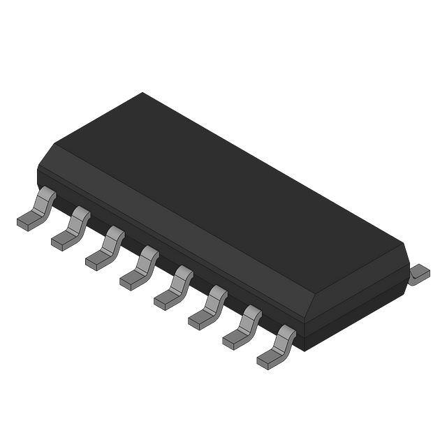
0.3" DIP-16 AND SO-16
±0.5LSB max INL AND DNL
72dB min SINAD
USES INTERNAL OR EXTERNAL
REFERENCE
MULTIPLE INPUT RANGES
35mW max POWER DISSIPATION
NO MISSING CODES
50µW POWER DOWN MODE
The ADS7812 is a low-power, single +5V supply, 12-bit
sampling analog-to-digital converter. It contains a complete
12-bit capacitor-based SAR A/D with a sample/hold, clock,
reference, and serial data interface.
The converter can be configured for a variety of input ranges
including ±10V, ±5V, 0V to 10V, and 0.5V to 4.5V. A high
impedance 0.3V to 2.8V input range is also available (input
impedance > 10MΩ). For most input ranges, the input
voltage can swing to +16.5V or –16.5V without damage to
the converter.
A flexible SPI compatible serial interface allows data to be
synchronized to an internal or external clock. The ADS7812
is specified at a 40kHz sampling rate over the –40°C to
+85°C temperature range. It is available in a 0.3" DIP-16 or
an SO-16 package.
APPLICATIONS
●
●
●
●
DATA ACQUISITION SYSTEMS
INDUSTRIAL CONTROL
TEST EQUIPMENT
DIGITAL SIGNAL PROCESSING
BUSY
PWRD
CONV
CS
Successive Approximation Register and Control Logic
40kΩ(1)
Clock
CDAC
R1IN
8kΩ(1)
EXT/INT
R2IN
Serial
20kΩ(1)
Data
Comparator
R3IN
BUF
CAP
DATACLK
Out
DATA
Buffer
4kΩ(1)
Internal
+2.5V Ref
NOTE: (1) Actual value may vary ±30%.
REF
Please be aware that an important notice concerning availability, standard warranty, and use in critical applications of
Texas Instruments semiconductor products and disclaimers thereto appears at the end of this data sheet.
All trademarks are the property of their respective owners.
Copyright © 1997-2003, Texas Instruments Incorporated
PRODUCTION DATA information is current as of publication date.
Products conform to specifications per the terms of Texas Instruments
standard warranty. Production processing does not necessarily include
testing of all parameters.
www.ti.com
�ELECTROSTATIC
DISCHARGE SENSITIVITY
ABSOLUTE MAXIMUM RATINGS(1)
Analog Inputs: R1IN ......................................................................... ±16.5V
R2IN ................................................ GND – 0.3V to +16.5V
R3IN ......................................................................... ±16.5V
REF ............................................ GND – 0.3V to VS + 0.3V
CAP ............................................... Indefinite Short to GND
Momentary Short to VS
VS ........................................................................................................... 7V
Digital Inputs ...................................................... GND – 0.3V to VS + 0.3V
Maximum Junction Temperature ................................................... +165°C
Internal Power Dissipation ............................................................. 825mW
Lead Temperature (soldering, 10s) ............................................... +300°C
This integrated circuit can be damaged by ESD. Texas Instruments recommends that all integrated circuits be handled with
appropriate precautions. Failure to observe proper handling
and installation procedures can cause damage.
ESD damage can range from subtle performance degradation
to complete device failure. Precision integrated circuits may be
more susceptible to damage because very small parametric
changes could cause the device not to meet its published
specifications.
NOTE: (1) Stresses above these ratings may cause permanent damage.
Exposure to absolute maximum conditions for extended periods may degrade
device reliability.
PACKAGE/ORDERING INFORMATION
PRODUCT
MINIMUM
MAXIMUM
SPECIFIED
SIGNAL-TOINTEGRAL
NO MISSING
(NOISE +
SPECIFIED
LINEARITY CODE LEVEL DISTORTION)
PACKAGE
TEMPERATURE
ERROR (LSB)
(LSB)
RATIO (DB) PACKAGE-LEAD DESIGNATOR(1)
RANGE
PACKAGE
MARKING
ORDERING
NUMBER
TRANSPORT
MEDIA, QUANTITY
ADS7812P
ADS7812PB
Tubes, 25
Tubes, 25
ADS7812P
ADS7812PB
±1
±0.5
12
12
70
72
Dip-16
N
"
"
ADS7812U
"
±1
"
12
"
70
"
SO-16
"
DW
"
–40°C to +85°C
"
ADS7812U
ADS7812U/1K
Tubes, 48
Tape and Reel, 1000
±0.5
"
12
"
72
"
SO-16
"
DW
"
–40°C to +85°C ADS7812UB
ADS7812UB
"
"
ADS7812UB/1K
Tubes, 48
Tape and Reel, 1000
ADS7812UB
"
–40°C to +85°C ADS7812P
"
ADS7812PB
ADS7812U
"
NOTE: (1) For the most current specifications and package information, refer to our web site at www.ti.com.
SPECIFICATIONS
At TA = –40°C to +85°C, fS = 40kHz, VS = +5V ±5%, using internal reference, unless otherwise specified.
ADS7812P, U
PARAMETER
CONDITIONS
MIN
TYP
RESOLUTION
DC ACCURACY
Integral Linearity Error
Differential Linearity Error
No Missing Codes
Transition Noise(2)
Full Scale Error(3)
Full Scale Error Drift
Full Scale Error(3)
Full Scale Error Drift
Bipolar Zero Error
Bipolar Zero Error Drift
Unipolar Zero Error
Unipolar Zero Error Drift
Recovery Time to Rated Accuracy
from Power Down(4)
Power Supply Sensitivity
AC ACCURACY
Spurious-Free Dynamic Range
Total Harmonic Distortion
Signal-to-(Noise+Distortion)
Signal-to-Noise
Useable Bandwidth(6)
Full Power –3dB Bandwidth
2
MAX
MIN
TYP
12
ANALOG INPUT
Voltage Range
Impedance
Capacitance
THROUGHPUT SPEED
Conversion Time
Complete Cycle
Throughput Rate
ADS7812PB, UB
20
25
0.1
0.1
Specified
0.05
±14
±5
±3
±3
300
1kHz
1kHz
1kHz
1kHz
±1
±1
✻
✻
✻
✻
±0.5
80
70
70
pF
✻
✻
µs
µs
kHz
±0.5
±0.5
LSB(1)
LSB
±0.25
✻
±0.5
±0.25
✻
±10
✻
✻
±6
✻
✻
✻
±0.75
+4.75V < (VS = +5V) < +5.25
fIN =
fIN =
fIN =
fIN =
Bits
✻
40
Ext. 2.5000V Ref
Ext. 2.5000V Ref
Bipolar Ranges
Bipolar Ranges
Unipolar Ranges
Unipolar Ranges
1.0µF Capacitor to CAP
UNITS
✻
✻
✻
✻
See Table I
See Table I
35
Acquire and Convert
MAX
98
–96
74
74
130
600
✻
✻
–80
72
72
✻
✻
✻
✻
✻
✻
✻
LSB
%
ppm/°C
%
ppm/°C
mV
ppm/°C
mV
ppm/°C
µs
LSB
dB(5)
dB
dB
dB
kHz
kHz
ADS7812
www.ti.com
SBAS042A
�SPECIFICATIONS (Cont.)
At TA = –40°C to +85°C, fS = 40kHz, VS = +5V ±5%, using internal reference, unless otherwise specified.
ADS7812P, U
PARAMETER
SAMPLING DYNAMICS
Aperture Delay
Aperture Jitter
Transient Response
Overvoltage Recovery(7)
REFERENCE
Internal Reference Voltage
Internal Reference Source Current
Internal Reference Drift
External Reference Voltage Range
External Reference Current Drain
CONDITIONS
Output Capacitance
POWER SUPPLY
VS
Power Dissipation
TEMPERATURE RANGE
Specified Performance
Derated Performance
TYP
2.48
2.3
2.5
100
8
2.5
VREF = +2.5V
–0.3
+2.0
ISINK = 1.6mA
ISOURCE = 500µA
High-Z State,
VOUT = 0V to VS
High-Z State
MAX
MIN
TYP
2.52
✻
2.7
100
✻
+0.8
VS +0.3V
±10
±10
✻
✻
✻
✻
✻
✻
Serial
Binary Two’s Complement
+0.4
✻
±1
+4
15
+4.75
fS = 40kHz
–40
–55
+5
MAX
✻
✻
✻
✻
40
20
5
750
FS Step
DIGITAL INPUTS
Logic Levels
VIL
VIH(8)
IIL
IIH
DIGITAL OUTPUTS
Data Format
Data Coding
VOL
VOH
Leakage Current
MIN
ADS7812PB, UB
+5.25
35
✻
+85
+125
✻
✻
✻
UNITS
ns
ps
µs
ns
✻
✻
✻
V
µA
ppm/°C
V
µA
✻
✻
✻
✻
V
V
µA
µA
✻
✻
V
V
µA
15
pF
✻
✻
V
mW
✻
✻
°C
°C
✻ Same specification as grade to the left.
NOTES: (1) LSB means Least Significant Bit. For the ±10V input range, one LSB is 4.88mV. (2) Typical rms noise at worst case transitions and temperatures.
(3) Full scale error is the worst case of –Full Scale or +Full Scale untrimmed deviation from ideal first and last code transitions, divided by the transition voltage
(not divided by the full-scale range) and includes the effect of offset error. (4) After the ADS7812 is initially powered on and fully settles, this is the time delay after
it is brought out of Power Down Mode until all internal settling occurs and the analog input is acquired to rated accuracy, and normal conversions can begin again.
(5) All specifications in dB are referred to a full-scale input. (6) Useable Bandwidth defined as Full-Scale input frequency at which Signal-to-(Noise+Distortion)
degrades to 60dB, or 10 bits of accuracy. (7) Recovers to specified performance after 2 x FS input overvoltage. (8) The minimum VIH level for the DATACLK signal
is 3V.
ADS7812
SBAS042A
www.ti.com
3
�PIN CONFIGURATION
PIN #
NAME
DESCRIPTION
1
R1IN
Analog Input. See Tables I and IV.
2
GND
Ground
3
R2IN
Analog Input. See Tables I and IV.
4
R3IN
Analog Input. See Tables I and IV.
5
BUF
Reference Buffer Output. Connect to R1IN, R2IN, or R3IN, as needed.
6
CAP
Reference Buffer Compensation Node. Decouple to ground with a 1µF tantalum capacitor in parallel with a 0.01µF ceramic capacitor.
7
REF
Reference Input/Output. Outputs internal +2.5V reference via a series 4kΩ resistor. Decouple this voltage with a 1µF to 2.2µF
tantalum capacitor to ground. If an external reference voltage is applied to this pin, it will override the internal reference.
8
GND
9
DATACLK
Data Clock Pin. With EXT/INT LOW, this pin is an output and provides the synchronous clock for the serial data. The output
is tri-stated when CS is HIGH. With EXT/INT HIGH, this pin is an input and the serial data clock must be provided externally.
Ground
10
DATA
Serial Data Output. The serial data is always the result of the last completed conversion and is synchronized to DATACLK.
If DATACLK is from the internal clock (EXT/INT LOW), the serial data is valid on both the rising and falling edges of DATACLK.
DATA is tri-stated when CS is HIGH.
11
EXT/INT
External or Internal DATACLK Pin. Selects the source of the synchronous clock for serial data. If HIGH, the clock must be
provided externally. If LOW, the clock is derived from the internal conversion clock. Note that the clock used to time the
conversion is always internal regardless of the status of EXT/INT.
12
CONV
Convert Input. A falling edge on this input puts the internal sample/hold into the hold state and starts a conversion regardless
of the state of CS. If a conversion is already in progress, the falling edge is ignored. If EXT/INT is LOW, data from the previous
conversion will be serially transmitted during the current conversion.
13
CS
Chip Select. This input tri-states all outputs when HIGH and enables all outputs when LOW. This includes DATA, BUSY, and
DATACLK (when EXT/INT is LOW). Note that a falling edge on CONV will initiate a conversion even when CS is HIGH.
14
BUSY
Busy Output. When a conversion is started, BUSY goes LOW and remains LOW throughout the conversion. If EXT/INT is
LOW, data is serially transmitted while BUSY is LOW. BUSY is tri-stated when CS is HIGH.
15
PWRD
Power Down Input. When HIGH, the majority of the ADS7812 is placed in a low power mode and power consumption is
significantly reduced. CONV must be taken LOW prior to PWRD going LOW in order to achieve the lowest power
consumption. The time required for the ADS7812 to return to normal operation after power down depends on a number of
factors. Consult the Power Down section for more information.
16
VS
+5V Supply Input. For best performance, decouple to ground with a 0.1µF ceramic capacitor in parallel with a 10µF tantalum
capacitor.
PIN CONFIGURATION
Top View
4
DIP, SOIC
ANALOG
INPUT
RANGE (V)
CONNECT
R1IN
TO
CONNECT
R2IN
TO
CONNECT
R3IN
TO
INPUT
IMPEDANCE
(kΩ)
±10V
VIN
BUF
GND
45.7
0.3125V to
2.8125V
VIN
VIN
VIN
> 10,000
26.7
R1IN
1
16 VS
GND
2
15 PWRD
±5V
GND
BUF
VIN
R2IN
3
14 BUSY
0V to 10V
BUF
GND
VIN
26.7
0V to 4V
BUF
VIN
GND
21.3
±3.33V
VIN
BUF
VIN
21.3
0.5V to
4.5V
GND
VIN
GND
21.3
R3IN
4
13 CS
BUF
5
12 CONV
CAP
6
11 EXT/INT
REF
7
10 DATA
GND
8
9
ADS7812
TABLE I. ADS7812 Input Ranges.
DATACLK
ADS7812
www.ti.com
SBAS042A
�TYPICAL PERFORMANCE CURVES
At TA = +25°C, fS = 40kHz, VS = +5V, ±10V input range, using internal reference, unless otherwise noted.
FREQUENCY SPECTRUM
(8192 Point FFT; fIN = 9.8kHz, 0dB)
0
0
–20
–20
–40
–40
Amplitude (dB)
–60
–80
–60
–80
–100
–100
–120
–120
5
10
15
0
20
5
10
20
Frequency (kHz)
SNR AND SINAD vs TEMPERATURE
(fIN = 1kHz, 0dB)
SFDR AND THD vs TEMPERATURE
(fIN = 1kHz, 0dB)
77
100
76
99
75
98
–98
97
–97
96
–96
74
73
SNR and SINAD
72
–100
–99
SFDR
THD
95
71
–95
94
–50
–25
0
25
50
75
100
–94
–50
–25
0
Temperature (°C)
25
50
75
100
75
100
Temperature (°C)
SIGNAL-TO-(NOISE + DISTORTION)
vs INPUT FREQUENCY (fIN = 0dB)
INTERNAL REFERENCE VOLTAGE
vs TEMPERATURE
74.0
2.515
2.510
Internal Reference (V)
73.8
SINAD (dB)
15
Frequency (kHz)
SFDR (dB)
SNR and SINAD (dB)
0
THD (dB)
Amplitude (dB)
FREQUENCY SPECTRUM
(8192 Point FFT; fIN = 980Hz, 0dB)
73.6
73.4
73.2
2.505
2.500
2.495
2.490
73.0
2.485
100
1k
10k
20k
–50
Input Signal Frequency (Hz)
0
25
50
Temperature (°C)
ADS7812
SBAS042A
–25
www.ti.com
5
�TYPICAL PERFORMANCE CURVES
(CONT)
At TA = +25°C, fS = 40kHz, VS = +5V, ±10V input range, using internal reference, unless otherwise noted.
ILE AND DLE AT +25°C
0.1
0.1
ILE (LSB)
0.2
0
–0.1
0
–0.1
–0.2
–0.2
0.2
0.2
0.1
0.1
DLE (LSB)
DLE (LSB)
ILE (LSB)
ILE AND DLE AT –40°C
0.2
0
–0.1
–0.2
800h
C00h
000h
400h
0
–0.1
–0.2
800h
7FFh
C00h
Hex BTC Code
7FFh
1
0.1
Linearity Degradation (LSB/LSB)
ILE (LSB)
0.2
0
–0.1
–0.2
0.2
DLE (LSB)
400h
POWER SUPPLY RIPPLE SENSITIVITY
ILE/DLE DEGRADATION PER LSB OF P-P RIPPLE
ILE AND DLE AT +85°C
0.1
0
10–1
10–2
ILE
10–3
10–4
DLE
10–5
–0.1
101
–0.2
800h
000h
Hex BTC Code
C00h
000h
400h
7FFh
102
103
104
105
106
107
Power Supply Ripple Frequency (Hz)
Hex BTC Code
6
ADS7812
www.ti.com
SBAS042A
�BASIC OPERATION
EXTERNAL DATACLK
Figure 1b shows a basic circuit to operate the ADS7812 with
a ±10V input range. To begin a conversion, a falling edge
must be provided to the CONV input. BUSY will go LOW
indicating that a conversion has started and will stay LOW
until the conversion is complete. Just prior to BUSY rising
near the end of the conversion, the internal working register
holding the conversion result will be transferred to the
internal shift register.
The internal shift register is clocked via the DATACLK
input. The recommended method of reading the conversion
result is to provide the serial clock after the conversion has
completed. See External DATACLK under the Reading
Data section of this data sheet for more information.
INTERNAL DATACLK
Figure 1a shows a basic circuit to operate the ADS7812 with
a ±10V input range. To begin a conversion and serial
transmission of the results from the previous conversion, a
falling edge must be provided to the CONV input. BUSY
will go LOW indicating that a conversion has started and
will stay LOW until the conversion is complete. During the
conversion, the results of the previous conversion will be
transmitted via DATA while DATACLK provides the synchronous clock for the serial data. The data format is 12-bit,
Binary Two’s Complement, and MSB first. Each data bit is
valid on both the rising and falling edge of DATACLK.
BUSY is LOW during the entire serial transmission and can
be used as a frame synchronization signal.
C2
C1
0.1µF 10µF
ADS7812
±10V
C3
1µF
+
C4
0.01µF
C5
1µF
+
1
R1IN
VS 16
2
GND
PWRD 15
3
R2IN
BUSY 14
4
R3IN
CS 13
5
BUF
CONV 12
6
CAP
EXT/INT 11
7
REF
DATA 10
8
GND
DATACLK
+5V
+
Frame Sync (optional)
Convert Pulse
40ns min
9
FIGURE 1a. Basic Operation, ±10V Input Range, Internal DATACLK.
C1
C2
0.1µF 10µF
ADS7812
±10V
C3
1µF
+
C4
0.01µF
C5
1µF
+
1
R1IN
VS 16
2
GND
PWRD 15
3
R2IN
BUSY 14
4
R3IN
CS 13
5
BUF
CONV 12
6
CAP
EXT/INT 11
7
REF
DATA 10
8
GND
DATACLK
9
+5V
+
Interrupt (optional)
Chip Select (optional(1))
Convert Pulse
+5V
40ns min
External Clock
NOTE: (1) Tie CS to GND if the outputs will always be active.
FIGURE 1b. Basic Operation, ±10V Input Range, External DATACLK.
ADS7812
SBAS042A
www.ti.com
7
�SYMBOL
DESCRIPTION
t1
Conversion Plus Acquisition Time
25
µs
t2
CONV LOW to All Digital
Inputs Stable
8
µs
STARTING A CONVERSION
MIN TYP MAX UNITS
t3
CONV LOW to Initiate a Conversion
40
ns
t4
BUSY Rising to Any Digital
Input Active
0
ns
t5
CONV HIGH Prior to Start
of Conversion
2
µs
t6
BUSY LOW
15
20
µs
t7
CONV LOW to BUSY LOW
85
120
ns
t8
Aperture Delay
40
t9
Conversion Time
14
20
µs
t10
Conversion Complete to
BUSY Rising
1.1
2
µs
5
µs
t11
Acquisition Time
t12
CONV LOW to Rising Edge
of First DATACLK
If a conversion is not currently in progress, a falling edge on
the CONV input places the sample and hold into the hold
mode and begins a conversion, as shown in Figure 2 and
with the timing given in Table II. During the conversion, the
CONV input is ignored. Starting a conversion does not
depend on the state of CS. A conversion can be started once
every 25µs (40kHz maximum conversion rate). There is no
minimum conversion rate.
Even though the CONV input is ignored while a conversion
is in progress, this input should be held static during the
conversion period. Transitions on this digital input can
easily couple into sensitive analog portions of the converter,
adversely affecting the conversion results (see the Sensitivity to External Digital Signals section of this data sheet for
more information).
Ideally, the CONV input should go LOW and remain LOW
throughout the conversion. It should return HIGH sometime
after BUSY goes HIGH. In addition, it should be HIGH
prior to the start of the next conversion for a minimum time
period given by t5. This will ensure that the digital transition
on the CONV input will not affect the signal that is acquired
for the next conversion.
An acceptable alternative is to return the CONV input HIGH
as soon as possible after the start of the conversion. For
example, a negative going pulse 100ns wide would make a
good CONV input signal. It is strongly recommended that
from time t2 after the start of a conversion until BUSY rises,
the CONV input should be held static (either HIGH or
LOW). During this time, the converter is more sensitive to
external noise.
ns
µs
1.4
t13
Internal DATACLK HIGH
250
350
500
t14
Internal DATACLK LOW
600
760
875
ns
t15
Internal DATACLK Period
t16
DATA Valid to Internal
DATACLK Rising
20
ns
t17
Internal DATACLK Falling
to DATA Not Valid
400
ns
t18
Falling Edge of Last DATACLK
to BUSY Rising
t19
External DATACLK Rising
to DATA Not Valid
t20
External DATACLK Rising
to DATA Valid
ns
µs
1.1
800
ns
15
ns
55
85
ns
t21
External DATACLK HIGH
50
ns
t22
External DATACLK LOW
50
ns
t23
External DATACLK Period
100
ns
t24
CONV LOW to External
DATACLK Active
120
ns
t25
External DATACLK LOW
or CS HIGH to BUSY Rising
2
µs
t26
CS LOW to Digital Outputs Enabled
85
ns
t27
CS HIGH to Digital Outputs Disabled
85
ns
TABLE II. ADS7812 Timing. TA = –40°C to +85°C.
t1
t2
t3
t4
t5
CONV
t6
t7
BUSY
t8
t10
t9
MODE
Acquire
t11
Convert
Acquire
Convert
FIGURE 2. Basic Conversion Timing.
8
ADS7812
www.ti.com
SBAS042A
�DESCRIPTION
DIGITAL OUTPUT
ANALOG INPUT
BINARY TWO’S COMPLEMENT
±10V
4.88mV
0.5V to 4.5V
0.98mV
9.99512V
0V
Full-Scale Range
Least Significant Bit (LSB)
+Full Scale –1LSB
BINARY CODE
HEX CODE
4.49902V
0111 1111 1111
7FF
2.5V
0000 0000 0000
000
–4.88mV
2.49902 V
1111 1111 1111
FFF
–10V
0.5V
1000 0000 0000
800
Midscale
Midscale –1LSB
–Full Scale
TABLE III. Ideal Input Voltage and Corresponding Digital Output for Two Common Input Ranges.
Converter Core
REF
CDAC
CONV
Clock
Control Logic
BUSY
Each flip-flop in the
working register is
latched as the
conversion proceeds
Working Register
D
Q
D
Q
D
Q
D
Q
D
Q
•••
W0
W1
W2
W10
W11
Update of the shift
register occurs just prior
to BUSY Rising(1)
Shift Register
D
Q
D
Q
D
Q
D
Q
D
Q
D
DATA
Q
EXT/INT
S0
S1
S2
S10
S11
SOUT
Delay
DATACLK
CS
NOTE: (1) If EXT/INT is HIGH (external clock), DATACLK is HIGH, and CS is LOW
during this time, the shift register will not be updated and the conversion result will be lost.
FIGURE 3. Block Diagram of the ADS7812’s Digital Inputs and Outputs.
READING DATA
CONV
t25
t6 – t25
BUSY
NOTE: Update of the internal shift register occurs in the
shaded region. If EXT/INT is HIGH, then DATACLK
must be LOW or CS must be HIGH during this time.
FIGURE 4. Timing of the Shift Register Update.
The ADS7812’s digital output is in Binary Two’s Complement (BTC) format. Table III shows the relationship between the digital output word and the analog input voltage
under ideal conditions.
Figure 3 shows the relationship between the various digital
inputs, digital outputs, and internal logic of the ADS7812.
Figure 4 shows when the internal shift register of the
ADS7812 is updated and how this relates to a single conversion cycle. Together, these two figures point out a very
important aspect of the ADS7812: the conversion result is
not available until after the conversion is complete. The
implications of this are discussed in the following sections.
ADS7812
SBAS042A
www.ti.com
9
�INTERNAL DATACLK
With EXT/INT tied LOW, the result from conversion ‘n’ is
serially transmitted during conversion ‘n+1’, as shown in
Figure 5 and with the timing given in Table II. Serial
transmission of data occurs only during a conversion. When
a transmission is not in progress, DATA and DATACLK are
LOW.
During the conversion, the results of the previous conversion will be transmitted via DATA, while DATACLK
provides the synchronous clock for the serial data. The data
format is 12-bit, Binary Two’s Complement, and MSB first.
Each data bit is valid on both the rising and falling edges of
DATACLK. BUSY is LOW during the entire serial transmission and can be used as a frame synchronization signal.
EXTERNAL DATACLK
With EXT/INT tied HIGH, the result from conversion ‘n’ is
clocked out after the conversion has completed, during the
next conversion (‘n+1’), or a combination of these two.
Figure 6 shows the case of reading the conversion result
after the conversion is complete. Figure 7 describes reading
the result during the next conversion. Figure 8 combines the
important aspects of Figures 6 and 7 as to reading part of the
result after the conversion is complete and the remainder
during the next conversion.
The serial transmission of the conversion result is initiated
by a rising edge on DATACLK. The data format is 12-bit,
Binary Two’s Complement, and MSB first. Each data bit is
valid on the falling edge of DATACLK. In some cases, it
t1
CONV
BUSY
t13
t12
t15
DATACLK
1
2
t18
3
t16
10
11
12
1
Bit 2
Bit 1
LSB
t14
t17
DATA
MSB
Bit 10
Bit 9
MSB
FIGURE 5. Serial Data Timing, Internal Clock (EXT/INT and CS LOW).
t1
t5
CONV
BUSY
t21
t4
DATACLK
t23
1
2
3
t19
4
10
11
12
t22
t20
DATA
MSB
Bit 10
Bit 9
Bit 2
Bit 1
LSB
FIGURE 6. Serial Data Timing, External Clock, Clocking After the Conversion Completes (EXT/INT HIGH, CS LOW).
10
ADS7812
www.ti.com
SBAS042A
�External DATACLK Active After the Conversion
The preferred method of obtaining the conversion result is to
provide the DATACLK signal after the conversion has been
completed and before the next conversion starts—as shown
in Figure 6. Note that the DATACLK signal should be static
before the start of the next conversion. If this is not observed, the DATACLK signal could affect the voltage that
is acquired.
might be possible to use the rising edge of the DATACLK
signal. However, one extra clock period (not shown in
Figures 6, 7, and 8) is needed for the final bit.
The external DATACLK signal must be LOW or CS must
be HIGH prior to BUSY rising (see time t25 in Figures 7 and
8). If this is not observed, the output shift register of the
ADS7812 will not be updated with the conversion result.
Instead, the previous contents of the shift register will
remain and the new result will be lost.
If more than 12 clock cycles are provided to the DATACLK
input, the DATA output will go LOW after the rising edge
of the 13th clock period. The operation of the ADS7812 will
not be affected as long as the timing specifications are met.
Before reading the next three paragraphs, consult the Sensitivity to External Digital Signals section of this data sheet.
This will explain many of the concerns regarding how and
when to apply the external DATACLK signal.
External DATACLK Active During the Next Conversion
Another method of obtaining the conversion result is shown
in Figure 7. Since the output shift register is not updated until
the end of the conversion, the previous result remains valid
during the next conversion. If a fast clock (≥ 2MHz) can be
provided to the ADS7812, the result can be read during time
t2. During this time, the noise from the DATACLK signal is
less likely to affect the conversion result.
t1
t2
CONV
BUSY
t21
t24
t23
DATACLK
1
2
3
t19
t25
4
11
12
1
t22
t20
DATA
MSB
Bit 10
Bit 9
Bit 1
LSB
MSB
FIGURE 7. Serial Data Timing, External Clock, Clocking During the Next Conversion (EXT/INT HIGH,
CS LOW).
CONV
BUSY
t5
t24
t4
DATACLK
DATA
1
2
MSB
n
Bit 10
t25
n+1
Bit n
Bit n-1
11
12
Bit 1
LSB
FIGURE 8. Serial Data Timing, External Clock, Clocking After the Conversion Completes and During the Next Conversion
(EXT/INT HIGH, CS LOW).
ADS7812
SBAS042A
www.ti.com
11
�External DATACLK Active After the Conversion
and During the Next Conversion
Figure 8 shows a method that is a hybrid of the two previous
approaches. This method works very well for microcontrollers
that do serial transfers 8 bits at a time and for slower
microcontrollers. For example, if the fastest serial clock that
the microcontroller can produce is 1µs, and two 8-bit transfers must be used to obtain the serial data, the approach
shown in Figure 6 would result in a diminished throughput
(26kHz maximum conversion rate). The method described
in Figure 7 could not be used because time t25 would be
violated. The approach in Figure 8 results in an improved
throughput rate (33kHz maximum with a 1µs clock) and
DATACLK is LOW during t25.
CHIP SELECT (CS)
The CS input allows the digital outputs of the ADS7812 to
be disabled and gates the external DATACLK signal when
EXT/INT is HIGH. See Figure 9 for the enable and disable
time associated with CS and Figure 3 for a block diagram of
the ADS7812’s logic. The digital outputs can be disabled at
any time.
Note that a conversion is initiated on the falling edge of CONV
even if CS is HIGH. If the EXT/INT input is LOW (internal
DATACLK) and CS is HIGH during the entire conversion, the
previous conversion result will be lost (the serial transmission
occurs but DATA and DATACLK are disabled).
CS
COMPATIBILITY WITH THE ADS7813
The only difference between the ADS7812 and the ADS7813
is in the internal control logic and the digital interface. Since
the ADS7813 is a 16-bit converter, the internal shift register
is 16 bits wide. In addition, only 16-bit decisions are made
during the conversion. Thus, the ADS7813’s conversion
time is approximately 133% of the ADS7812’s.
The timing presented in this data sheet will allow as much
compatibility as possible with the ADS7813. The main
concern will be the different number of serial clocks. If a
design must be compatible with both the ADS7812 and
ADS7813, it is recommended to consider the ADS7813
first. If the design works with the ADS7813, it will certainly
work with the ADS7812. This is also true in regards to
layout (see the Layout section of this data sheet).
ANALOG
INPUT
RANGE (V)
CONNECT
R1IN
TO
CONNECT
R2IN
TO
0.3125 to 2.8125
VIN
–0.417 to 2.916
VIN
0.417 to 3.750
±3.333
t26
BUSY, DATA,
DATACLK(1)
t27
HI-Z
Active
HI-Z
NOTE: (1) DATACLK is an output only when EXT/INT is LOW.
FIGURE 9. Enable and Disable Timing for Digital Outputs.
ANALOG INPUT
The ADS7812 offers a number of input ranges. This is
accomplished by connecting the three input resistors to
either the analog input (VIN), to ground (GND), or to the
2.5V reference buffer output (BUF). Table I shows the
input ranges that are typically used in data acquisition
applications. These ranges are all specified to meet the
specifications given in the Specifications table. Table IV
contains a complete list of ideal input ranges, associated
input connections, and comments regarding the range.
CONNECT
R3IN
TO
INPUT
IMPEDANCE
(kΩ)
VIN
VIN
> 10,000
VIN
BUF
26.7
VIN
VIN
GND
26.7
Offset and gain not specified
VIN
BUF
VIN
21.3
Specified offset and gain
–15 to 5
VIN
BUF
BUF
45.7
Offset and gain not specified
±10
VIN
BUF
GND
45.7
Specified offset and gain
0.833 to 7.5
VIN
GND
VIN
21.3
Offset and gain not specified
–2.5 to 17.5
VIN
GND
BUF
45.7
Exceeds absolute maximum VIN
2.5 to 22.5
VIN
GND
GND
45.7
Exceeds absolute maximum VIN
0 to 2.857
BUF
VIN
VIN
45.7
Offset and gain not specified
VIN cannot go below GND – 0.3V
COMMENT
Specified offset and gain
VIN cannot go below GND – 0.3V
–1 to 3
BUF
VIN
BUF
21.3
0 to 4
BUF
VIN
GND
21.3
Specified offset and gain
–6.25 to 3.75
BUF
BUF
VIN
26.7
Offset and gain not specified
Specified offset and gain
0 to 10
BUF
GND
VIN
26.7
0.357 to 3.214
GND
VIN
VIN
45.7
Offset and gain not specified
–0.5 to 3.5
GND
VIN
BUF
21.3
VIN cannot go below GND – 0.3V
0.5 to 4.5
GND
VIN
GND
21.3
Specified offset and gain
±5
GND
BUF
VIN
26.7
Specified offset and gain
1.25 to 11.25
GND
GND
VIN
26.7
Offset and gain not specified
TABLE IV. Complete List of Ideal Input Ranges.
12
ADS7812
www.ti.com
SBAS042A
�The other three input ranges involve the connection at R2IN
being driven below GND – 0.3V. This input has a reversebiased ESD protection diode connection to ground. If R2IN
is taken below ground, this diode will be forward-biased and
will clamp the negative input at –0.4V to –0.7V, depending
on the temperature. Here again, these ranges can still be used
at the cost of the full-scale range of the converter.
Note that Table IV assumes that the voltage at the REF pin
is 2.5V. This is true if the internal reference is being used or
if the external reference is 2.5V. Other reference voltages
will change the values in Table IV.
HIGH IMPEDANCE MODE
When R1IN, R2IN, and R3IN are connected to the analog input,
the input range of the ADS7812 is 0.3125V to 2.8125V and
the input impedance is greater than 10MΩ. This input range
can be used to connect the ADS7812 directly to a wide
variety of sensors. Figure 10 shows the impedance of the
sensor versus the change in ILE and DLE of the ADS7812.
The performance of the ADS7812 can be improved for higher
sensor impedance by allowing more time for acquisition. For
example, 10µs of acquisition time will approximately double
sensor impedance for the same ILE/DLE performance.
The input impedance and capacitance of the ADS7812 are
very stable with temperature. Assuming that this is true of
the sensor as well, the graph shown in Figure 10 will vary
less than a few percent over the specified temperature range
of the ADS7812. If the sensor impedance varies significantly with temperature, the worst-case impedance should
be used.
DRIVING THE ADS7812 ANALOG INPUT
In general, any “reasonably fast”, high quality operational or
instrumentation amplifier can be used to drive the ADS7812
input. When the converter enters the acquisition mode, there
is some charge injection from the converter’s input to the
amplifier’s output. This can result in inadequate settling
time with slower amplifiers. Be very careful with singlesupply amplifiers, particularly if their output will be required to swing very close to the supply rails.
In addition, be careful in regards to the amplifier’s linearity.
The outputs of single-supply and “rail-to-rail” amplifiers
can saturate as they approach the supply rails. Rather than
the amplifier’s transfer function being a straight line, the
curve can become severely ‘S’ shaped. Also, watch for the
point where the amplifier switches from sourcing current to
sinking current. For some amplifiers, the transfer function
can be noticeably discontinuous at this point, causing a
significant change in the output voltage for a much smaller
change on the input.
Texas Instruments manufactures a wide variety of operational and instrumentation amplifiers that can be used to
drive the input of the ADS7812. These include the OPA627,
OPA134, OPA132, and INA110.
REFERENCE
The ADS7812 can be operated with its internal 2.5V reference or an external reference. By applying an external
reference voltage to the REF pin, the internal reference
voltage is overdriven. The voltage at the REF input is
internally buffered by a unity gain buffer. The output of this
buffer is present at the BUF and CAP pins.
REF
The REF pin is the output of the internal 2.5V reference or
the input for an external reference. A 1µF to 2.2µF tantalum
capacitor should be connected between this pin and ground.
The capacitor should be placed as close as possible to the
ADS7812.
When using the internal reference, the REF pin should not
be connected to any type of significant load. An external
load will cause a voltage drop across the internal 4kΩ
resistor that is in series with the internal reference. Even a
4MΩ external load to ground will cause a decrease in the
full-scale range of the converter by 4 LSBs.
LINEARITY ERROR vs SOURCE IMPEDANCE
Change in Worst-Case
Linearity Error (LSBs)
The input impedance results from the various connections
and the internal resistor values (refer to the block diagram on
the front page of this data sheet). The internal resistor values
are typical and can change by ±30%, due to process variations. However, the ratio matching of the resistors is considerably better than this. Thus, the input range will vary only
a few tenths of a percent from part to part, while the input
impedance may vary up to ±30%.
The Specifications table contains the maximum limits for
the variation of the analog input range, but only for those
ranges where the comment field shows that the offset and
gain are specified (this includes all the ranges listed in Table
I). For the other ranges, the offset and gain are not tested and
are not specified.
Five of the input ranges in Table IV are not recommended
for general use. For two of the these, the input voltage
exceeds the absolute maximum. These ranges can still be
used as long as the input voltage remains under the absolute
maximum, but this will moderately to significantly reduce
the full-scale range of the converter.
TA = +25°C
Acquisition Time = 5µs
DLE
ILE
0
1
2
3
4
5
6
7
8
9 10 11 12 13 14 15
External Source Impedance (kΩ)
FIGURE 10. Linearity Error vs Source Impedance in the High
Impedance Mode (R1IN = R2IN = R3IN = VIN).
ADS7812
SBAS042A
0.60
0.55
0.50
0.45
0.40
0.35
0.30
0.25
0.20
0.15
0.10
0.05
0.00
www.ti.com
13
�CAP
The CAP pin is used to compensate the internal reference
buffer. A 1µF tantalum capacitor in parallel with a 0.01µF
ceramic capacitor should be connected between this pin and
ground, with the ceramic capacitor placed as close as possible to the ADS7812. The total value of the capacitance on
the CAP pin is critical to optimum performance of the
ADS7812. A value larger than 2.0µF could overcompensate
the buffer while a value lower than 0.5µF may not provide
adequate compensation.
BUF
The voltage on the BUF pin is the output of the internal
reference buffer. This pin is used to provide +2.5V to the
analog input or inputs for the various input configurations.
The BUF output can provide up to 1mA of current to an
external load. The load should be constant as a variable load
could affect the conversion result by modulating the BUF
voltage. Also note that the BUF output will show significant
glitches as each bit decision is made during a conversion.
Between conversions, the BUF output is quiet.
POWER DOWN
The ADS7812 has a power-down mode that is activated by
taking CONV LOW and then PWRD HIGH. This will
power down all of the analog circuitry including the reference, reducing power dissipation to under 50µW. To exit the
power-down mode, CONV is taken HIGH and then PWRD
is taken LOW. Note that a conversion will be initiated if
PWRD is taken HIGH while CONV is LOW.
While in the power-down mode, the voltage on the capacitors connected to CAP and REF will begin to leak off. The
voltage on the CAP capacitor leaks off much more rapidly
than the REF capacitor (the REF input of the ADS7812
becomes high impedance when PWDN is HIGH—this is not
true for the CAP input). When the power-down mode is
exited, these capacitors must be allowed to recharge and
settle to a 12-bit level. Figure 11 shows the amount of time
typically required to obtain a valid 12-bit result based on the
amount of time spent in power down (at room temperature).
This figure assumes that the total capacitance on the CAP
pin is 1.01µF.
Figure 12 provides a circuit which can significantly reduce
the power up time if the power down time will be fairly brief
(a few seconds or less). A low on-resistance MOSFET is
used to disconnect the capacitance on the CAP pin from the
leakage paths internal to the ADS7812. This allows the
capacitors to retain their charge for a much longer period of
time, reducing the time required to recharge them at power
up. With this circuit, the power down time can be extended
to tens or hundreds of milliseconds with almost instantaneous power up.
POWER-DOWN TO POWER-UP RESPONSE
Power-Up Time to Rated Accuracy (µs)
The range for the external reference is 2.3V to 2.7V. The
voltage on REF determines the full-scale range of the converter and the corresponding LSB size. Increasing the reference voltage will increase the LSB size in relation to the
internal noise sources which, in turn, can improve signal-tonoise ratio. Likewise, decreasing the reference voltage will
reduce the LSB size and signal-to-noise ratio.
300
TA = +25°C
250
200
150
100
50
0
0.1
1
10
100
Power-Down Duration (ms)
FIGURE 11. Power-Down to Power-Up Response.
1RF7604
+
1µF
1
8
1
R1IN
VS 16
2
7
2
GND
PWRD 15
3
6
3
R2IN
BUSY 14
4
5
4
R3IN
CS 13
5
BUF
CONV 12
6
CAP
EXT/INT 11
7
REF
DATA 10
8
GND
0.01µF
DATACLK
Power-Down Signal
9
FIGURE 12. Improved Power-Up Response Circuit.
14
ADS7812
www.ti.com
SBAS042A
�LAYOUT
For example, the timing diagram in Figure 2 shows that the
CONV signal should return HIGH sometime during time t2.
In fact, the CONV signal can return HIGH at any time
during the conversion. However, after time t2, the transition
of the CONV signal has the potential of creating a good deal
of noise on the ADS7812 die. If this transition occurs at just
precisely the wrong time, the conversion results could be
affected. In a similar manner, transitions on the DATACLK
input could affect the conversion result.
For the ADS7812, there are 12 separate bit decisions which
are made during the conversion. The most significant bit
decision is made first, proceeding to the least significant bit
at the end of the conversion. Each bit decision involves the
assumption that the bit being tested should be set. This is
combined with the result that has been achieved so far. The
converter compares this combined result with the actual
input voltage. If the combined result is too high, the bit is
cleared. If the result is equal to or lower than the actual input
voltage, the bit remains HIGH. This is why the basic
architecture is referred to as “successive approximation
register.”
If the result so far is getting very close to the actual input
voltage, then the comparison involves two voltages which are
very close together. The ADS7812 has been designed so that
the internal noise sources are a minimum just prior to the
comparator result being latched. However, if a external digital
signal transitions at this time, a great deal of noise will be
coupled into the sensitive analog section of the ADS7812.
Even if this noise produces a difference between the two
voltages of only 2mV, the conversion result will be off by 3
counts or least significant bits (LSBs). (The internal LSB size
of the ADS7812 is 610µV regardless of the input range.)
Once a digital transition has caused the comparator to make
a wrong bit decision, the decision cannot be corrected. All
subsequent bit decisions will then be wrong (unless some
type of error correction is employed). Figure 13 shows a
successive approximation process that has gone awry. The
dashed line represents what the correct bit decisions should
have been. The solid line represents the actual result of the
conversion.
The ADS7812 should be treated as a precision analog
component and should reside completely on the “analog”
portion of the printed circuit board. Ideally, a ground plane
should extend underneath the ADS7812 and under all other
analog components. This plane should be separate from the
digital ground until they are joined at the power supply
connection. This will help prevent dynamic digital ground
currents from modulating the analog ground through a
common impedance to power ground.
The +5V power should be clean, well-regulated, and separate from the +5V power for the digital portion of the design.
One possibility is to derive the +5V supply from a linear
regulator located near the ADS7812. If derived from the
digital +5V power, a 5Ω to 10Ω resistor should be placed in
series with the power connection from the digital supply. It
may also be necessary to increase the bypass capacitance
near the VS pin (an additional 100µF or greater capacitor in
parallel with the 10µF and 0.1µF capacitors). For designs
with a large number of digital components or very high
speed digital logic, this simple power supply filtering scheme
may not be adequate.
SENSITIVITY TO EXTERNAL
DIGITAL SIGNALS
All successive approximation register-based A/D converters
are sensitive to external sources of noise. The reason for this
will be explained in the following paragraphs. For the
ADS7812 and similar A/D converters, this noise most often
originates due to the transition of external digital signals.
While digital signals that run near the converter can be the
source of the noise, the biggest problem occurs with the
digital inputs to the converter itself.
In many cases, the system designer may not be aware that
there is a problem or a potential for a problem. For a 12-bit
system, these problems typically occur at the least significant
bits and only at certain places in the converter’s transfer
function. For a 16-bit converter, the problem can be much
easier to spot.
External Noise
SAR Operation after
Wrong Bit Decision
Actual Input
Voltage
Converter’s
Full-Scale
Input Voltage
Range
Proper SAR Operation
Internal DAC
Voltage
Wrong Bit Decision Made Here
t
Conversion Clock
Conversion Start
(Hold Mode)
1
1
0
0
0
0
Incorrect Result
(1
0
1
1
0
1)
Correct Result
FIGURE 13. SAR Operation When External Noise Affects the Conversion.
ADS7812
SBAS042A
www.ti.com
15
�Keep in mind that the time period when the comparator is
most sensitive to noise is fairly small. Also, the peak portion
of the noise “event” produced by a digital transition is fairly
brief as most digital signals transition in a few nanoseconds.
The subsequent noise may last for a period of time longer
than this and may induce further effects which require a
longer settling time; however, in general, the event is over
within a few tens of nanoseconds.
For the ADS7812, error correction is done when the tenth bit
is decided. During this bit decision, it is possible to correct
limited errors that may have occurred during previous bit
decisions. However, after the tenth bit, no such correction is
possible. Note that for the timing diagrams shown in Figures
2, 5, 6, 7, and 8, all external digital signals should remain
static from 8µs after the start of a conversion until BUSY
rises. The tenth bit is decided approximately 10µs to 11µs
into the conversion.
three converters. After the conversions are finished, each
result is transferred, in turn. The QSPI port is completely
programmable to handle the timing and transfers without
processor intervention. If the CONV signal is generated in
this way, it should be possible to make both AC and DC
measurements with the ADS7812, as the CONV signal will
have low jitter. Note that if the CONV signal is generated via
software commands, it will have a good deal of jitter and
only low frequency (DC) measurements can be made.
QSPI
+5V
ADS7812
PCS0
CONV
PCS1
CS
EXT/INT
PCS2
PCS3
SCK
DATACLK
MIS0
DATA
APPLICATIONS INFORMATION
+5V
ADS7812
QSPI INTERFACING
Figure 14 shows a simple interface between the ADS7812
and any queued serial peripheral interface (QSPI) equipped
microcontroller (available on several Motorola devices).
This interface assumes that the convert pulse does not
originate from the microcontroller and that the ADS7812 is
the only serial peripheral.
Before enabling the QSPI interface, the microcontroller must
be configured to monitor the slave select (SS) line. When a
LOW to HIGH transition occurs (indicating the end of a
conversion), the port can be enabled. If this is not done, the
microcontroller and A/D converter may not be properly synchronized. (The slave select line simply enables communication—it does not indicate the start or end of a serial transfer.)
EXT/INT
CS
DATACLK
DATA
+5V
ADS7812
CONV
EXT/INT
CS
DATACLK
DATA
FIGURE 15. QSPI Interface to the Three ADS7812s.
DSP56002 INTERFACING
The DSP56002 serial interface has an serial peripheral
interface (SPI) compatibility mode with some enhancements. Figure 16 shows an interface between the ADS7812
and the DSP56002. As with the QSPI interface of Figure 14,
Convert Pulse
QSPI
CONV
ADS7812
CONV
PCS0/SS
BUSY
MOSI
DATA
SCK
Convert Pulse
DSP56002
CONV
CS
EXT/INT
CPOL = 0 (Inactive State is LOW)
CPHA = 1 (Data valid on falling edge)
QSPI port is in slave mode.
SC1
BUSY
SRD
DATA
SCO
DATACLK
CS
FIGURE 14. QSPI Interface to the ADS7812.
Figure 15 shows a QSPI-equipped microcontroller interfacing to three ADS7812s. There are many possible variations
to this interface scheme. As shown, the QSPI port produces
a common CONV signal which initiates a conversion on all
16
ADS7812
DATACLK
SYN = 0 (Asychronous)
GCK = 1 (Gated clock)
SCD1 = 0 (SC1 is an input)
SHFD = 0 (Shift MSB first)
WL1 = 0 WL0 = 1 (Word length = 12 bits)
EXT/INT
FIGURE 16. DSP56002 Interface to the ADS7812.
ADS7812
www.ti.com
SBAS042A
�the DSP56002 must be programmed to enable the serial
interface when a LOW to HIGH transition on SCI occurs.
The DSP56002 can also provide the CONV signal, as shown
in Figure 17. The receive and transmit sections of the
interface are decoupled (asynchronous mode) and the transmit section is set to generate a word length frame sync every
other transmit frame (frame rate divider set to 2). The
prescale modulus should be set to produce a transmit frame
at twice the desired conversion rate.
APPLICATIONS CIRCUIT
Figure 18 shows a multiplexed data acquisition circuit using
the ADS7812. The MPC508A provides the multiplexing
function while the OPA134 is configured as a Sallen-Key,
two-pole, unity gain lowpass filter.
DSP56002
ADS7812
SC2
CONV
BUSY
SC0
DATACLK
SRD
DATA
CS
SYN = 0 (Asychronous)
GCK = 1 (Gated clock)
SCD2 = 1 (SC2 is an output)
SHFD = 0 (Shift MSB first)
WL1 = 0 WL0 = 1 (Word length = 12 bits)
EXT/INT
FIGURE 17. DSP56002 Interface to the ADS7812. Processor Initiates Conversions.
+15V
C1
2.2nF
MPC508A
In 1
R1
1.4kΩ
In 2
±10V
Full Scale
R2
15.4kΩ
In 3
OPA134
C2
330pF
In 4
–15V
In 5
In 6
A0
In 7
A1
In 8
A2
ADS7812
R1IN
BUSY
R2IN
CONV
R3IN
DATA
BUF
DATACLK
µP
FIGURE 18. Multiplexed Data Acquisition Circuit.
ADS7812
SBAS042A
www.ti.com
17
�PACKAGE OPTION ADDENDUM
www.ti.com
27-Feb-2020
PACKAGING INFORMATION
Orderable Device
Status
(1)
Package Type Package Pins Package
Drawing
Qty
Eco Plan
Lead/Ball Finish
MSL Peak Temp
(2)
(6)
(3)
Op Temp (°C)
Device Marking
(4/5)
ADS7812PB
ACTIVE
PDIP
N
16
25
Green (RoHS
& no Sb/Br)
NIPDAU
N / A for Pkg Type
ADS7812P
B
ADS7812UB
ACTIVE
SOIC
DW
16
40
Green (RoHS
& no Sb/Br)
NIPDAU-DCC
Level-3-260C-168 HR
-40 to 85
ADS7812U
B
ADS7812UB/1K
ACTIVE
SOIC
DW
16
1000
Green (RoHS
& no Sb/Br)
NIPDAU-DCC
Level-3-260C-168 HR
-40 to 85
ADS7812U
B
ADS7812UBG4
ACTIVE
SOIC
DW
16
40
Green (RoHS
& no Sb/Br)
NIPDAU-DCC
Level-3-260C-168 HR
-40 to 85
ADS7812U
B
(1)
The marketing status values are defined as follows:
ACTIVE: Product device recommended for new designs.
LIFEBUY: TI has announced that the device will be discontinued, and a lifetime-buy period is in effect.
NRND: Not recommended for new designs. Device is in production to support existing customers, but TI does not recommend using this part in a new design.
PREVIEW: Device has been announced but is not in production. Samples may or may not be available.
OBSOLETE: TI has discontinued the production of the device.
(2)
RoHS: TI defines "RoHS" to mean semiconductor products that are compliant with the current EU RoHS requirements for all 10 RoHS substances, including the requirement that RoHS substance
do not exceed 0.1% by weight in homogeneous materials. Where designed to be soldered at high temperatures, "RoHS" products are suitable for use in specified lead-free processes. TI may
reference these types of products as "Pb-Free".
RoHS Exempt: TI defines "RoHS Exempt" to mean products that contain lead but are compliant with EU RoHS pursuant to a specific EU RoHS exemption.
Green: TI defines "Green" to mean the content of Chlorine (Cl) and Bromine (Br) based flame retardants meet JS709B low halogen requirements of