�������
�� ��
�����
�
� � ��� ������� ���
ADS7864
SBAS141A – SEPTEMBER 2000 – REVISED MARCH 2005
500kHz, 12-Bit, 6-Channel Simultaneous Sampling
ANALOG-TO-DIGITAL CONVERTER
FEATURES
DESCRIPTION
•
•
•
•
•
•
•
•
The ADS7864 is a dual 12-bit, 500kHz
analog-to-digital (A/D) converter with 6 fully differential input channels grouped into three pairs for high
speed simultaneous signal acquisition. Inputs to the
sample-and-hold amplifiers are fully differential and
are maintained differential to the input of the A/D
converter. This provides excellent common-mode rejection of 80dB at 50kHz which is important in high
noise environments.
6 Simultaneous Sampling Channels
Fully Differential Inputs
2µs Total Throughput per Channel
No Missing Codes
Parallel Interface
1MHz Effective Sampling Rate
Low Power: 50mW
6X FIFO
The ADS7864 offers a parallel interface and control
inputs to minimize software overhead. The output
data for each channel is available as a 16-bit word
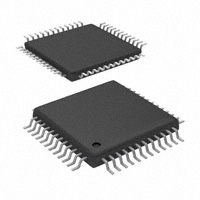
(address and data). The ADS7864 is offered in a
TQFP-48 package and is fully specified over the
–40°C to +85°C operating range.
APPLICATIONS
•
•
•
Motor Control
Multi-Axis Positioning Systems
3-Phase Power Control
HOLDA
HOLDB
CH A0+
CH A0−
SAR
S/H
Amp
CH B0+
COMP
CH B0−
S/H
Amp
HOLDC
Interface
A2
CDAC
A1
CH C1+
CH C1−
S/H
Amp
A0
Conversion
and
MUX
BYTE
Control
CLOCK
REFIN
CS
RD
Internal
2.5V
Reference
REFOUT
BUSY
RESET
FIFO
Registers
CH A1+
CH A1−
Channel/
Data Output
COMP
S/H
Amp
CDAC
CH B1+
CH B1−
16
S/H
Amp
CH C1+
CH C1−
S/H
Amp
MUX
SAR
Please be aware that an important notice concerning availability, standard warranty, and use in critical applications of Texas
Instruments semiconductor products and disclaimers thereto appears at the end of this data sheet.
PRODUCTION DATA information is current as of publication date.
Products conform to specifications per the terms of the Texas
Instruments standard warranty. Production processing does not
necessarily include testing of all parameters.
Copyright © 2000–2005, Texas Instruments Incorporated
�ADS7864
www.ti.com
SBAS141A – SEPTEMBER 2000 – REVISED MARCH 2005
This integrated circuit can be damaged by ESD. Texas Instruments recommends that all integrated
circuits be handled with appropriate precautions. Failure to observe proper handling and installation
procedures can cause damage.
ESD damage can range from subtle performance degradation to complete device failure. Precision
integrated circuits may be more susceptible to damage because very small parametric changes could
cause the device not to meet its published specifications.
ORDERING INFORMATION (1)
PRODUCT
MINIMUM
RELATIVE
ACCURACY (LSB)
MAXIMUM
GAIN
ERROR (%)
PACKAGELEAD
PACKAGE
DESIGNATOR
SPECIFIED
TEMPERATURE
RANGE
ADS7864Y
±2
±0.75
TQFP-48
PFB
–40°C to +85°C
ADS7864YB
(1)
±1
±0.5
TQFP-48
PFB
ORDERING
NUMBER
TRANSPORT MEDIA,
QUANTITY
ADS7864Y
Tape and Reel, 250
ADS7864Y
Tape and Reel, 2000
ADS7864YB
Tape and Reel, 250
ADS7864YB
Tape and Reel, 2000
–40°C to +85°C
For the most current package and ordering information, see the Package Option Addendum at the end of this document, or see the TI
website at www.ti.com.
ABSOLUTE MAXIMUM RATINGS
over operating free-air temperature range (unless otherwise noted)
ADS7864
UNIT
Analog Inputs to AGND: Any Channel Input
–0.3 to (+VD + 0.3)
V
Analog Inputs to AGND: REFIN
–0.3 to (+VD + 0.3)
V
Digital Inputs to DGND
–0.3 to (+VD + 0.3)
V
Ground Voltage Differences: AGND, DGND
±0.3
V
Ground Voltage Differences: +VD to AGND
–0.3 to +6
V
Power Supply Difference: +VA, +VD
±0.3
V
Power Dissipation
325
mW
Maximum Junction Temperature
+150
°C
Operating Temperature Range
–40 to +85
°C
Storage Temperature Range
–65 to +150
°C
+300
°C
Lead Temperature (soldering, 10s)
2
�ADS7864
www.ti.com
SBAS141A – SEPTEMBER 2000 – REVISED MARCH 2005
44
43
42
41
40
39
CH A0−
CH B0+
CH B0−
CH C0+
CH C0−
CH C1−
CH C1+
CH B1−
CH B1+
38
37
CH A1−
45
CH A1+
46
+VA
36
AGND
AGND
35
3
DB15
REFIN
34
4
DB14
REFOUT
33
5
DB13
RESET
32
6
DB12
A0
31
7
DB11
A1
30
8
DB10
A2
29
1
+VA
2
0.1µF
0.1µF
+
10µF
+5V
Analog Power
Supply
Global Reset
ADS7864Y
DB6
HOLDC
25
13
14
15
16
17
18
19
20
21
CS
12
CLOCK
26
RD
HOLDB
DGND
DB7
+VD
11
BUSY
27
DB1
28
HOLDA
DB0
BYTE
DB8
DB3
DB9
DB2
9
10
DB5
22
23
24
Address Select
Sample and Hold
Inputs
+5V
Digital Power Supply
Chip Select
Read Input
Data Ouput
Clock Input
0.1µF
BUSY Output
10µF
+
47
DB4
+5V
Analog Power
Supply
48
CH A0+
BASIC OPERATION
+
10µF
DGND
AGND
3
�ADS7864
www.ti.com
SBAS141A – SEPTEMBER 2000 – REVISED MARCH 2005
ELECTRICAL CHARACTERISTICS
All specifications TMIN to TMAX, +VA = +VD = +5V, VREF = internal +2.5V and fCLK = 8MHz, fSAMPLE = 500kHz (unless otherwise
noted).
PARAMETER
TEST CONDITIONS
ADS7864Y
MIN
TYP
Resolution
ADS7864YB
MAX
MIN
TYP
12
MAX
12
UNIT
Bits
Analog Input
Input Voltage Range-Bipolar
Absolute Input Range
VCENTER = +2.5V
–VREF
+VREF
+IN
–0.3
+VA + 0.3
–IN
–0.3
+VA + 0.3
Input Capacitance
Input Leakage Current
CLK = GND
–VREF
+VREF
V
V
V
15
15
pF
±1
±1
µA
System Performance
No Missing Codes
12
Integral Linearity
Integral Linearity Match
–0.9
Referenced to REFIN
±0.75
±4
Referenced to REFIN
±0.15
±0.75
Referenced to REFIN
±0.15
±0.75
±1
±0.5
LSB
±3
3
±0.1
±0.5
±0.1
±0.5
3
3
LSB
LSB
±0.4
3
Negative Gain Error Match
Common-Mode Rejection Ratio
–0.9
3
Positive Gain Error Match
Negative Gain Error
Bits
±0.5
0.5
±0.6
Bipolar Offset Error Match
Positive Gain Error
2
0.5
Differential Linearity
Bipolar Offset Error
12
±0.75
3
LSB
LSB
% of FSR
LSB
% of FSR
LSB
At DC
84
84
VIN = ±1.25VPP at 50kHz
80
80
dB
Noise
120
120
µVRMS
Power Supply Rejection Ratio
0.3
2
0.3
dB
2
LSB
Sampling Dynamics
Conversion Time per A/D
1.75
1.75
Acquisition Time
0.25
0.25
Throughput Rate
500
µs
µs
500
kHz
Aperture Delay
3.5
3.5
ns
Aperture Delay Matching
100
100
ps
Aperture Jitter
50
50
ps
Small-Signal Bandwidth
40
40
MHz
Dynamic Characteristics
Total Harmonic Distortion
VIN = ±2.5VPP at 100kHz
–75
–75
dB
SINAD
VIN = ±2.5VPP at 100kHz
71
71
dB
Spurious Free Dynamic Range
VIN = ±2.5VPP at 100kHz
78
78
dB
Channel-to-Channel Isolation
VIN = ±2.5VPP at 50kHz
–76
–76
dB
Voltage Reference
Internal Reference Voltage
2.475
2.5
2.525
2.475
2.5
2.525
V
Internal Drift
10
10
ppm/°C
Internal Noise
µVPP
50
50
Internal Source Current
2
2
Internal Load Rejection
0.005
0.005
80
80
Internal PSRR
External Reference Voltage Range
1.2
2.5
Input Current
Input Capacitance
4
2.6
1.2
2.5
100
5
5
mA
mV/µA
dB
2.6
V
100
µA
pF
�ADS7864
www.ti.com
SBAS141A – SEPTEMBER 2000 – REVISED MARCH 2005
ELECTRICAL CHARACTERISTICS (continued)
All specifications TMIN to TMAX, +VA = +VD = +5V, VREF = internal +2.5V and fCLK = 8MHz, fSAMPLE = 500kHz (unless otherwise
noted).
PARAMETER
ADS7864Y
TEST CONDITIONS
MIN
ADS7864YB
TYP
MAX
MIN
TYP
MAX
UNIT
Digital Input/Output
Logic Family
CMOS
CMOS
Logic Levels:
VIH
IIH = +5µA
3.0
+VD + 0.3
3.0
+VD + 0.3
V
VIL
IIL = +5µA
–0.3
0.8
–0.3
0.8
V
VOH
IOH = –500µA
3.5
VOL
IOL = –500µA
3.5
V
0.4
External Clock
0.2
Data Format
8
Binary Two's Complement
0.4
0.2
8
V
MHz
Binary Two's Complement
Power-Supply Requirements
Power Supply Voltage, +VA, +VD
4.75
5
5.25
4.75
5
5.25
V
Quiescent Current, +VA, +VD
10
10
mA
Power Dissipation
50
50
mW
CH A0+
CH A0−
CH B0+
CH B0−
CH C0+
CH C0−
CH C1−
CH C1+
CH B1−
CH B1+
CH A1−
CH A1+
PIN CONFIGURATIONS
48
47
46
45
44
43
42
41
40
39
38
37
+VA
1
36 +VA
AGND
2
35 AGND
DB15
3
34 REFIN
DB14
4
33 REFOUT
DB13
5
32 RESET
DB12
6
31 A0
ADS7864
DB11
7
30 A1
DB10
8
29 A2
DB9
9
28 BYTE
13
14
15
16
17
18
19
20
21
22
23
24
DB0
BUSY
DGND
+VD
CLOCK
RD
CS
25 HOLDC
DB1
DB6 12
DB2
26 HOLDB
DB3
DB7 11
DB4
27 HOLDA
DB5
DB8 10
5
�ADS7864
www.ti.com
SBAS141A – SEPTEMBER 2000 – REVISED MARCH 2005
PIN DESCRIPTIONS
6
PIN
NAME
1
+VA
DESCRIPTION
2
AGND
Analog Ground
3
DB15
Data Valid Output: ‘1’ for data valid; ‘0’ for invalid data.
4
DB14
Channel Address Output Pin (see Table 2)
5
DB13
Channel Address Output Pin (see Table 2)
6
DB12
Channel Address Output Pin (see Table 2)
7
DB11
Data Bit 11 - MSB
8
DB10
Data Bit 10
9
DB9
Data Bit 9
10
DB8
Data Bit 8
11
DB7
Data Bit 7
12
DB6
Data Bit 6
13
DB5
Data Bit 5
14
DB4
Data Bit 4
15
DB3
Data Bit 3
16
DB2
Data Bit 2
17
DB1
Data Bit 1
18
DB0
Data Bit 0 - LSB
19
BUSY
Low when a conversion is in progress.
20
DGND
Digital Ground
21
+VD
22
CLOCK
23
RD
RD Input. Enables the parallel output when used in conjunction with chip select.
24
CS
Chip Select
25
HOLDC
Places Channels C0 and C1 in hold mode.
26
HOLDB
Places Channels B0 and B1 in hold mode.
27
HOLDA
Places Channels A0 and A1 in hold mode.
28
BYTE
29
A2
A2 Address/Mode Select Pin (see Table 3).
30
A1
A1 Address/Mode Select Pin (see Table 3).
31
A0
A0 Address/Mode Select Pin (see Table 3).
32
RESET
33
REFOUT
34
REFIN
Reference In
35
AGND
Analog Ground
36
+VA
37
CH A1+
Noninverting Input Channel A1
38
CH A1–
Inverting Input Channel A1
39
CH B1+
Noninverting Input Channel B1
40
CH B1–
Inverting Input Channel B1
41
CH C1+
Noninverting Input Channel C1
42
CH C1–
Inverting Input Channel C1
43
CH C0–
Inverting Input Channel C0
44
CH C0+
Noninverting Input Channel C0
45
CH B0–
Inverting Input Channel B0
46
CH B0+
Noninverting Input Channel B0
47
CH A0–
Inverting Input Channel A0
48
CH A0+
Noninverting Input Channel A0
Analog Power Supply. Normally +5V.
Digital Power Supply, +5VDC
An external clock must be applied to the CLOCK input.
2 × 8 Output Capability. Active high.
Reset Pin
Reference Out
Analog Power Supply. Normally +5V.
�ADS7864
www.ti.com
SBAS141A – SEPTEMBER 2000 – REVISED MARCH 2005
TYPICAL CHARACTERISTICS
All specifications TA = +25°C, +VA = +VD = +5V, VREF = internal +2.5V and fCLK = 8MHz, fSAMPLE = 500kHz (unless otherwise
noted)
FREQUENCY SPECTRUM
(4096 Point FFT; fIN = 199.9kHz, -0.2dB)
0
0
−20
−20
−40
−40
Amplitude (dB)
Amplitude (dB)
FREQUENCY SPECTRUM
(4096 Point FFT; fIN = 99.9kHz, –0.2dB)
−60
−80
−100
−60
−80
−100
−120
−120
0
62.5
125
187.5
250
0
62.5
125
Frequency (kHz)
Figure 1.
Figure 2.
SIGNAL-TO-NOISE RATIO AND
SIGNAL-TO-(NOISE+DISTORTION)
vs INPUT FREQUENCY
CHANGE IN SIGNAL-TO-NOISE RATIO
AND SIGNAL-TO-(NOISE+DISTORTION)
vs TEMPERATURE
75
Delta from +25�C (dB)
SNR and SINAD (dB)
70
SINAD
65
60
55
50
10k
100k
Input Frequency (Hz)
Figure 3.
250
1.0
SNR
1k
187.5
Frequency (kHz)
1M
0.6
0.2
SNR
−0.2
SINAD
−0.6
−1.0
−40
−20
0
20
40
60
80
Temperature (� C)
Figure 4.
7
�ADS7864
www.ti.com
SBAS141A – SEPTEMBER 2000 – REVISED MARCH 2005
TYPICAL CHARACTERISTICS (continued)
All specifications TA = +25°C, +VA = +VD = +5V, VREF = internal +2.5V and fCLK = 8MHz, fSAMPLE = 500kHz (unless otherwise
noted)
POSITIVE GAIN MATCH vs TEMPERATURE
(Maximum Deviation for All Six Channels)
1.0
1.80
Change in Positive Gain Match (LSB)
THD and SFDR Delta from +25� C (dB)
CHANGE IN SPURIOUS FREE DYNAMIC RANGE
AND TOTAL HARMONIC DISTORTION
vs TEMPERATURE
THD
0.5
0.0
SFDR
−0.5
−1.0
−40
−20
0
20
40
60
1.70
1.60
1.50
1.40
1.30
1.20
−40
80
−20
0
Temperature (�C)
Figure 5.
1.40
2.506
Reference (V)
Change in Negative Gain Match (LSB)
2.510
1.30
1.20
1.10
2.498
2.494
−20
0
20
40
60
2.490
−40
80
−20
0
1.0
1.20
CH1
CH0
0.6
20
40
Temperature (�C)
Figure 9.
60
80
BIPOLAR ZERO MATCH vs TEMPERATURE
1.30
60
80
Bipolar Match (LSB)
Bipolar Zero (LSB)
BIPOLAR ZERO vs TEMPERATURE
0
40
Figure 8.
1.2
−20
20
Temperature (� C)
Figure 7.
8
80
2.502
Temperature (�C)
0.4
−40
60
REFERENCE VOLTAGE vs TEMPERATURE
1.50
0.8
40
Figure 6.
NEGATIVE GAIN MATCH vs TEMPERATURE
(Maximum Deviation for All Six Channels)
1.00
−40
20
Temperature (� C)
1.10
1.00
0.90
−40
−20
0
20
40
Temperature (� C)
Figure 10.
60
80
�ADS7864
www.ti.com
SBAS141A – SEPTEMBER 2000 – REVISED MARCH 2005
TYPICAL CHARACTERISTICS (continued)
All specifications TA = +25°C, +VA = +VD = +5V, VREF = internal +2.5V and fCLK = 8MHz, fSAMPLE = 500kHz (unless otherwise
noted)
DIFFERENTIAL LINEARITY ERROR vs CODE
INTEGRAL LINEARITY ERROR vs CODE
2.0
1
Typical of All Six Channels
1.5
0.5
1.0
0.25
0.5
ILE (LSB)
DLE (LSB)
Typical of All Six Channels
0.75
0
−0.25
−0.5
−0.5
−1.0
−0.75
−1.5
−1
800
000
−2.0
800
7FF
7FF
Hex BTC Code
Figure 11.
Figure 12.
INTEGRAL LINEARITY ERROR vs TEMPERATURE
−0.02
2.0
1.6
−0.03
1.2
0.8
ILE (LSB)
−0.04
−0.05
−0.06
Positive ILE
0.4
0
−0.4
Negative ILE
−0.8
−1.2
−0.07
−0.08
−40
000
Hex BTC Code
INTEGRAL LINEARITY ERROR MATCH
vs TEMPERATURE
Channel A0/Channel C1
(Different Converter, Different Channels)
ILE Match (LSB)
0
−1.6
−2.0
−20
0
20
40
Temperature (� C)
Figure 13.
60
80
40
20
0
20
40
60
80
Temperature (� C)
Figure 14.
9
�ADS7864
www.ti.com
SBAS141A – SEPTEMBER 2000 – REVISED MARCH 2005
TYPICAL CHARACTERISTICS (continued)
All specifications TA = +25°C, +VA = +VD = +5V, VREF = internal +2.5V and fCLK = 8MHz, fSAMPLE = 500kHz (unless otherwise
noted)
INTEGRAL LINEARITY ERROR MATCH vs CODE
Channel A0/Channel B0
(Same Converter, Different Channels)
DIFFERENTIAL LINEARITY ERROR
vs TEMPERATURE
1.0
0.8
0.8
0.6
Positive DLE
0.6
0.4
0.2
ILE (LSB)
DLE (LSB)
0.4
0
−0.2
−0.4
0
−0.2
−0.4
Negative DLE
−0.6
−0.6
−0.8
−40
0.2
−0.8
−20
0
20
40
60
−1.0
800
80
Temperature (� C)
Figure 15.
−65
0.75
−70
0.5
−75
0.25
−80
dB
ILE (LSB)
CHANNEL SEPARATION
1.0
0
−0.25
−85
−90
−0.5
−95
−0.75
10
7FF
Figure 16.
INTEGRAL LINEARITY ERROR MATCH vs CODE
Channel A0/Channel B1
(Different Converter, Different Channels)
−1.0
800
000
Hex BTC Code
−100
000
7FF
1k
10k
Hex BTC Code
f IN (Hz)
Figure 17.
Figure 18.
100k
�ADS7864
www.ti.com
SBAS141A – SEPTEMBER 2000 – REVISED MARCH 2005
APPLICATIONS INFORMATION
INTRODUCTION
The ADS7864 is a high speed, low power, dual 12-bit
analog-to-digital converter (ADC) that operates from a
single +5V supply. The input channels are fully
differential with a typical common-mode rejection of
80dB. The part contains dual 2µs successive approximation ADCs, six differential sample-and-hold amplifiers, an internal +2.5V reference with REFIN and
REFOUT pins and a high speed parallel interface.
There are six analog inputs that are grouped into
three channels (A, B and C). Each A/D converter has
three inputs (A0/A1, B0/B1 and C0/C1) that can be
sampled and converted simultaneously, thus preserving the relative phase information of the signals
on both analog inputs. Each pair of channels has a
hold signal (HOLDA, HOLDB, HOLDC) to allow
simultaneous sampling on all six channels. The part
accepts an analog input voltage in the range of –VREF
to +VREF, centered around the internal +2.5V reference. The part will also accept bipolar input ranges
when a level shift circuit is used at the front end (see
Figure 25).
A conversion is initiated on the ADS7864 by bringing
the HOLDX pin low for a minimum of 15ns. HOLDX
low places both sample-and-hold amplifiers of the X
channels in the hold state simultaneously and the
conversion process is started on both channels. The
BUSY output will then go low and remain low for the
duration of the conversion cycle. The data can be
read from the parallel output bus following the conversion by bringing both RD and CS low.
Conversion time for the ADS7864 is 1.75µs when an
8MHz external clock is used. The corresponding
acquisition time is 0.25µs. To achieve maximum
output rate (500kHz), the read function can be
performed during at the start of the next conversion.
NOTE: This mode of operation is described in more
detail in the Timing and Control section of this data
sheet.
signal, is 5ns. The average delta of repeated aperture
delay values is typically 50ps (also known as aperture
jitter). These specifications reflect the ability of the
ADS7864 to capture AC input signals accurately at
the exact same moment in time.
REFERENCE
Under normal operation, the REFOUT pin (pin 2)
should be directly connected to the REFIN pin (pin 1)
to provide an internal +2.5V reference to the
ADS7864. The ADS7864 can operate, however, with
an external reference in the range of 1.2V to 2.6V for
a corresponding full-scale range of 2.4V to 5.2V.
The internal reference of the ADS7864 is
double-buffered. If the internal reference is used to
drive an external load, a buffer is provided between
the reference and the load applied to pin 33 (the
internal reference can typically source 2mA of current—load capacitance should not exceed 100pF). If
an external reference is used, the second buffer
provides isolation between the external reference and
the CDAC. This buffer is also used to recharge all of
the capacitors of both CDACs during conversion.
ANALOG INPUT
The analog input is bipolar and fully differential. There
are two general methods of driving the analog input
of the ADS7864: single-ended or differential (see
Figure 19 and Figure 20). When the input is
single-ended, the –IN input is held at the common-mode voltage. The +IN input swings around the
same common voltage and the peak-to-peak amplitude is the (common-mode +VREF) and the
(common-mode –VREF). The value of VREF determines
the range over which the common-mode voltage may
vary (see Figure 21).
−VREF to +VREF
peak−to−peak
Common
Voltage
SAMPLE-AND-HOLD SECTION
The sample-and-hold amplifiers on the ADS7864
allow the ADCs to accurately convert an input sine
wave of full-scale amplitude to 12-bit accuracy. The
input bandwidth of the sample-and-hold is greater
than the Nyquist rate of the ADC (Nyquist equals
one-half of the sampling rate) even when the ADC is
operated at its maximum throughput rate of 500kHz.
The typical small-signal bandwidth of the
sample-and-hold amplifiers is 40MHz.
Typical aperture delay time, or the time it takes for
the ADS7864 to switch from the sample to the hold
mode following the negative edge of the HOLDX
ADS7864
Single−Ended Input
VREF
peak−to−peak
Common
Voltage
ADS7864
VREF
peak−to−peak
Differential Input
Figure 19. Methods of Driving the ADS7864
Single-Ended or Differential
11
�ADS7864
www.ti.com
SBAS141A – SEPTEMBER 2000 – REVISED MARCH 2005
+IN
CM +VREF
+VREF
CM Voltage
−IN = CM Voltage
−VREF
CM −VREF
CM +1/2VREF
t
Single−Ended Inputs
+IN
+VREF
CM Voltage
CM −1/2VREF
−VREF
−IN
t
Differential Inputs
NOTES: Common−Mode Voltage (Differential Mode) =
(IN+) − (IN−)
, Common−Mode Voltage (Single−Ended Mode) = IN−.
2
The maximum differential voltage between +IN and −IN of the ADS7864 is VREF. See Figures 21 and 22 for a further
explanation of the common voltage range for single−ended and differential inputs.
Figure 20. Using the ADS7864 in the Single-Ended and Differential Input Modes
5
5
VCC = 5V
4.7
VCC = 5V
4.1
4
4
3
Single−Ended Input
Common Voltage Range (V)
Common Voltage Range (V)
4.05
2.7
2.3
2
1
0.9
0
2
0.90
1
0.3
−1
1.2
1.5
2.0
2.6
2.5
3.0
VREF (V)
Figure 21. Single-Ended Input: Common-Mode Voltage
Range vs VREF
12
Differential Input
0
−1
1.0
3
1.2
1.0
1.5
2.0
2.6
2.5
VREF (V)
Figure 22. Differential Input: Common-Mode
Voltage Range vs VREF
3.0
�ADS7864
www.ti.com
SBAS141A – SEPTEMBER 2000 – REVISED MARCH 2005
In each case, care should be taken to ensure that the
output impedance of the sources driving the +IN and
–IN inputs are matched. Otherwise, this may result in
offset error, which will change with both temperature
and input voltage.
The input current on the analog inputs depend on a
number of factors: sample rate, input voltage, and
source impedance. Essentially, the current into the
ADS7864 charges the internal capacitor array during
the sampling period. After this capacitance has been
fully charged, there is no further input current. The
source of the analog input voltage must be able to
charge the input capacitance (15pF) to a 12-bit
settling level within two clock cycles. When the
converter goes into the hold mode, the input impedance is greater than 1GΩ.
8000
7000
Number of Conversions
When the input is differential, the amplitude of the
input is the difference between the +IN and –IN input,
or: (+IN) – (–IN). The peak-to-peak amplitude of each
input is ±1/2VREF around this common voltage. However, since the inputs are 180° out of phase, the
peak-to-peak amplitude of the differential voltage is
+VREF to –VREF. The value of VREF also determines
the range of the voltage that may be common to both
inputs (see Figure 22).
6000
5000
4000
3000
2000
1000
0
2044
Figure 23 shows a histogram plot for the ADS7864
following 8,000 conversions of a DC input. The DC
input was set at output code 2046. All but one of the
conversions had an output code result of 2046 (one
of the conversions resulted in an output of 2047). The
histogram reveals the excellent noise performance of
the ADS7864.
2046
2047
2048
Code (decimal)
Figure 23. Histogram of 8,000 Conversions of a
DC Input
1.4V
3kΩ
Care must be taken regarding the absolute analog
input voltage. The +IN and –IN inputs should always
remain within the range of GND – 300mV to VDD +
300mV.
TRANSITION NOISE
2045
DATA
Test Point
100pF
CLOAD
VOH
DATA
VOL
tR
tF
Voltage Waveforms for DATA Rise and Fall Times t R, and t F.
Figure 24. Test Circuits for Timing Specifications
13
�ADS7864
www.ti.com
SBAS141A – SEPTEMBER 2000 – REVISED MARCH 2005
BIPOLAR INPUTS
The differential inputs of the ADS7864 were designed
to accept bipolar inputs (–VREF and +VREF) around the
internal reference voltage (2.5V), which corresponds
to a 0V to 5V input range with a 2.5V reference. By
using a simple op amp circuit featuring a single
amplifier and four external resistors, the ADS7864
can be configured to accept bipolar inputs. The
conventional ±2.5V, ±5V, and ±10V input ranges can
be interfaced to the ADS7864 using the resistor
values shown in Figure 25.
R1
Hold signals. The FIFO mode will allow the six
registers to be used by a single channel pair, and
therefore three locations for CH X0 and three locations for CH X1 can be acquired before they are
read from the part.
EXPLANATION OF CLOCK, RESET AND
BUSY PINS
CLOCK—An external clock has to be provided for the
ADS7864. The maximum clock frequency is 8MHz.
The minimum clock cycle is 125ns (see Figure 26, t5),
and the clock has to remain high (see Figure 26, t6)
or low (see Figure 26, t7) for at least 40ns.
4kΩ
CLOCK
OPA340
20kΩ
t6
−IN
Bipolar Input
t1
+IN
t7
t5
ADS7864
R2
t3
HOLDA
REFOUT (pin 33)
2.5V
BIPOLAR INPUT
R1
R2
±10V
±5V
±2.5V
1kΩ
2kΩ
4kΩ
5kΩ
10kΩ
20kΩ
HOLDB
t9
t2
HOLDC
Figure 25. Level Shift Circuit for Bipolar Input
Ranges
RESET
t8
TIMING AND CONTROL
The ADS7864 uses an external clock (CLOCK, pin
22) which controls the conversion rate of the CDAC.
With an 8MHz external clock, the A/D sampling rate
is 500kHz which corresponds to a 2µs maximum
throughput time.
THEORY OF OPERATION
The ADS7864 contains two 12-bit A/D converters that
operate simultaneously. The three hold signals
(HOLDA, HOLDB, HOLDC) select the input MUX and
initiate the conversion. A simultaneous hold on all six
channels can occur with all three hold signals strobed
together. The converted values are saved in six
registers. For each read operation the ADS7864
outputs 16 bits of information (12 Data, 3 Channel
Address and Data Valid). The Address/Mode signals
(A0, A1, A2) select how the data is read from the
ADS7864. These Address/Mode signals can define a
selection of a single channel, a cycle mode that
cycles through all channels or a FIFO mode that
sequences the data determined by the order of the
14
Figure 26. Start of the Conversion
RESET—Bringing reset low will reset the ADS7864. It
will clear all the output registers, stop any actual
conversions and will close the sampling switches.
Reset has to stay low for at least 20ns (see Figure 26, t8). The reset should be back high for at least
20ns (see Figure 26, t9), before starting the next
conversion (negative hold edge).
BUSY—Busy goes low when the internal A/D converters start a new conversion. It stays low as long as
the conversion is in progress (see Figure 27, 13
clock-cycles, t10) and rises again after the data is
latched to the output register. With Busy going high,
the new data can be read. It takes at least 16 clock
cycles (see Figure 27, t11) to complete conversion.
START OF A CONVERSION
By bringing one or all of the HOLDX signals low, the
input data of the corresponding channel X is immediately placed in the hold mode (5ns). The conversion
of this channel X follows as soon as the A/D
converter is available for the particular channel. If
�ADS7864
www.ti.com
SBAS141A – SEPTEMBER 2000 – REVISED MARCH 2005
other channels are already in the hold mode but not
converted, then the conversion of channel X is put in
the queue until the previous conversion has been
completed. If more than one channel goes into hold
mode within one clock cycle, then channel A will be
converted first if HOLDA is one of the triggered hold
signals. Next, channel B will be converted, and last,
channel C. If it is important to detect a hold command
during a certain clock cycle, then the falling edge of
the hold signal has to occur at least 10ns before the
falling edge of the clock. (see Figure 26, t1). The hold
signal can remain low without initiating a new conversion. The hold signal has to be high for at least 15ns
(see Figure 26, t2) before it is brought low again and
hold has to stay low for at least 20ns (see Figure 26,
t3).
In the example of Figure 26, the signal HOLDB goes
low first and channel B0 and B1 will be converted
first. The falling edges of HOLDA and HOLDC occur
within the same clock cycle. Therefore, the channels
A0 and A1 will be converted as soon as the channels
B0 and B1 are finished (plus acquisition time). When
the A-channels are finished, the C-channels will be
converted. The second HOLDA signal is ignored, as
the A-channels are not converted at this point in time.
Once a particular hold signal goes low, further impulses of this hold signal are ignored until the
conversion is finished or the part is reset. When the
conversion is finished (BUSY signal goes high), the
sampling switches will close and sample the selected
channel. The start of the next conversion must be
delayed to allow the input capacitor of the ADS7864
to be fully charged. This delay time depends on the
driving amplifier, but should be at least 175ns
(see Figure 27, t4).
The ADS7864 can also convert one channel continuously, as it is shown in Figure 27 with channel B.
Therefore, HOLDA and HOLDC are kept high all the
time. To gain acquisition time, the falling edge of
HOLDB takes place just before the falling edge of
clock. One conversion requires 16 clock cycles. Here,
data is read after the next conversion is initiated by
HOLDB. To read data from channel B, A1 is set high
and A2 is low. As A0 is low during the first reading
(A2 A1 A0 = 010) data B0 is put to the output. Before
the second RD, A0 switches high (A2 A1 A0 = 011)
so data from channel B1 is read.
Table 1. Timing Specifications
SYMBOL
DESCRIPTION
MIN
t1
HOLD (A, B, C) before falling edge of clock
10
TYP
MAX
UNITS
ns
t2
HOLD high time to be recognized again
15
ns
t3
HOLD low time
20
ns
t4
Input capacitor charge time
175
ns
t5
Clock period
125
ns
t6
Clock high time
40
ns
t7
Clock low time
40
ns
t8
Reset pulse width
20
ns
t9
First hold after reset
20
t10
Conversion time
t11
Successive conversion time (16 × t5)
2
µs
t12
Address setup before RD
10
ns
t13
CS before end of RD
30
ns
t14
RD high time
30
ns
ns
12.5 × t5
ns
15
�ADS7864
www.ti.com
SBAS141A – SEPTEMBER 2000 – REVISED MARCH 2005
t11
BUSY
t4
t10
CLOCK
HOLDB
CS
RD
A0
Figure 27. Timing of One Conversion Cycle
READING DATA (RD, CS)—In general, the channel/data outputs are in tristate. Both CS and RD have
to be low to enable these outputs. RD and CS have
to stay low together for at least 30ns (see Figure 28,
t13) before the output data is valid. RD has to remain
high for at least 30ns (see Figure 28, t14) before
bringing it back low for a subsequent read command.
12.5 clock-cycles after the start of a conversion
(BUSY going low), the new data is latched into its
output register. If a read process is initiated around
12.5 clock cycles after BUSY went low, RD and CS
should stay low for at least 50ns to get the new data
stored to its register and switched to the output.
CS being low tells the ADS7864 that the bus on the
board is assigned to the ADS7864. If an A/D converter shares a bus with digital gates, there is a
possibility that digital (high frequency) noise may be
coupled into the A/D converter. If the bus is just used
by the ADS7864, CS can be hardwired to ground.
Reading data at the falling edge of one of the hold
signals might cause distortion of the hold value.
BUSY
CLOCK
HOLDB
CS
RD
A0
t4
t1
t13
t14
t12
Figure 28. Timing for Reading Data
16
�ADS7864
www.ti.com
SBAS141A – SEPTEMBER 2000 – REVISED MARCH 2005
Table 2. Channel Truth Table
OUTPUT CODE (DB15…DB0)
The ADS7864 has a 16-bit output word. DB15 is ‘1’ if
the output contains valid data. This is important for
the FIFO mode. Valid Data can be read until DB15
switches to 0. DB14, DB13 and DB12 store channel
information as indicated in Table 2 (Channel Truth
Table). The 12-bit output data is stored from DB11
(MSB) to DB0 (LSB).
DATA CHANNEL
DB14
DB13
DB12
A0
0
0
0
A1
0
0
1
B0
0
1
0
B1
0
1
1
C0
1
0
0
C1
1
0
1
BYTE—If there is only an 8-bit bus available on a
board, then Byte can be set high (see Figure 29 and
Figure 30). In this case, the lower eight bits can be
read at the output pins DB7 to DB0 at the first RD
signal, and the higher bits after the second RD signal.
HOLDA
HOLDC
BUSY
CS
RD
BYTE
Figure 29. Reading Data in Cycling Mode
CS
RD
BYTE
A0
A0
A1
A1
B0
B0
LOW
HIGH
LOW
HIGH
LOW
HIGH
B1
C0
C1
A0
Figure 30. Reading Data in Cycling Mode
17
�ADS7864
www.ti.com
SBAS141A – SEPTEMBER 2000 – REVISED MARCH 2005
GETTING DATA
The ADS7864 has three different output modes that
are selected with A2, A1 and A0. A2A1A0 are only
active when RD and CS are both low. After a reset
occurs, A2A1A0 are set to 000.
With (A2 A1 A0) = 000 to 101 a particular channel
can directly be addressed (see Table 3 and Figure 27). The channel address should be set at least
10ns (see Figure 28, t12) before the falling edge of
RD and should not change as long as RD is low.
Table 3. Address/Mode Truth Table
CHANNEL
SELECTED/
MODE
A2
A1
A0
A0
0
0
0
A1
0
0
1
B0
0
1
0
B1
0
1
1
C0
1
0
0
C1
1
0
1
Cycle Mode
1
1
0
FIFO Mode
1
1
1
from channel A0 is read on the first RD signal, then
A1 on the second, followed by B0, B1, C0 and finally
C1 before reading A0 again. Data from channel A0 is
brought to the output first after a reset-signal or after
powering the part up.
The third mode is a FIFO mode that is addressed
with (A2 A1 A0 = 111). Data of the channel that is
converted first will be read first. So, if a particular
channel is most interesting and is converted more
frequently (e.g., to get a history of a particular
channel) then there are three output registers per
channel available to store data. When the ADS7864
is operated in the FIFO mode, an initial RD/CS is
necessary (after power up and after reset), so that
the internal address is set to ‘111’, before the first
conversion starts.
If a read process is just going on (RD signal low) and
new data has to be stored, then the ADS7864 will
wait until the read process is finished (RD signal
going high) before the new data gets latched into its
output register.
With (A2 A1 A0) = 110 the interface is running in a
cycle mode (see Figure 29 and Figure 30). Here, data
At time tA (see Figure 31) the ADS7864 resets. With
the reset signal, all conversions and scheduled conversions are cancelled. The data in the output registers are also cleared. With a reset, a running conversion gets interrupted and all channels go into the
sample mode again.
RESET
CLOCK
HOLDA
HOLDB
HOLDC
tA
tB
tC
tD tE
tF
Figure 31. Example of Hold Signals
18
�ADS7864
www.ti.com
SBAS141A – SEPTEMBER 2000 – REVISED MARCH 2005
At time tB a HOLDB signal occurs. With the next
falling clock edge (tC) the ADS7864 puts channel B
into the loop to be converted next. As the reset signal
occurred at tA, the conversion of channel B will be
started with the next rising edge of the clock after tC.
Bit 15 shows if the FIFO is empty (low) or if it
contains channel information (high). Bits 12 to 14
contain the Channel for the 12-bit data word (Bit 0 to
11). If the data is from channel A0, then bits 14 to 12
are ‘000’. The Channel bit pattern is outlined in
Table 2 (Channel Truth Table).
Within the next clock cycle (tC to tF), HOLDC (tD) and
HOLDA (tE) occur. If more than one hold signals get
active within one clock cycle, channel A will be
converted first. Therefore, as soon as the conversion
of channel B is done, the conversion of channel A will
be initiated. After this second conversion, channel C
will be converted.
New data is always written into the next available
register. At t0 (see Figure 32), the reset deletes all the
existing data. At t1 the new data of the channels A0
and A1 are put into registers 0 and 1. On t2 the read
process of channel A0 data is finished. Therefore,
this data is dumped and A1 data is shifted to register
0. At t3 new data is available, this time from channel
B0 and B1. This data is written into the next available
registers (register 1 and 2). The new data of channel
C0 and C1 at t4 is put on top (registers 3 and 4).
The 16 bit output word has following structure:
Valid Data
3-Bit Channel
Information
12-Bit Data Word
RESET
Conversion
Channel A
BUSY
Conversion
Channel B
Conversion
Channel C
RD
reg. 5
empty
empty
empty
empty
empty
reg. 4
empty
empty
empty
empty
ch C1
reg. 2
empty
empty
empty
empty
ch C0
reg. 3
empty
empty
empty
ch B1
ch B1
reg. 1
empty
ch A1
empty
ch B0
ch B0
reg. 0
empty
ch A0
ch A1
ch A1
ch A1
t0
t1
t2
t3
t4
Figure 32. Functionality Diagram of FIFO Registers
19
�ADS7864
www.ti.com
SBAS141A – SEPTEMBER 2000 – REVISED MARCH 2005
LAYOUT
For optimum performance, care should be taken with
the physical layout of the ADS7864 circuitry. This is
particularly true if the CLOCK input is approaching
the maximum throughput rate. The basic SAR architecture is sensitive to glitches or sudden changes on
the power supply, reference, ground connections and
digital inputs that occur just prior to latching the
output of the analog comparator. Thus, driving any
single conversion for an n-bit SAR converter, there
are n 'windows' in which large external transient
voltages can affect the conversion result. Such
glitches might originate from switching power
supplies, nearby digital logic or high power devices.
The degree of error in the digital output depends on
the reference voltage, layout, and the exact timing of
the external event. These errors can change if the
external event changes in time with respect to the
CLOCK input. With this in mind, power to the
ADS7864 should be clean and well-bypassed. A
0.1µF ceramic bypass capacitor should be placed as
close to the device as possible. In addition, a 1µF to
20
10µF capacitor is recommended. If needed, an even
larger capacitor and a 5Ω or 10Ω series resistor may
be used to low-pass filter a noisy supply. On average,
the ADS7864 draws very little current from an external reference as the reference voltage is internally
buffered. If the reference voltage is external and
originates from an op amp, make sure that it can
drive the bypass capacitor or capacitors without
oscillation. A bypass capacitor must not be used
when using the internal reference (tie pin 33 directly
to pin 34). The AGND and DGND pins should be
connected to a clean ground point. In all cases, this
should be the ‘analog’ ground. Avoid connections
which are too close to the grounding point of a
microcontroller or digital signal processor. If required,
run a ground trace directly from the converter to the
power supply entry point. The ideal layout will include
an analog ground plane dedicated to the converter
and associated analog circuitry.
�PACKAGE OPTION ADDENDUM
www.ti.com
14-Oct-2022
PACKAGING INFORMATION
Orderable Device
Status
(1)
Package Type Package Pins Package
Drawing
Qty
Eco Plan
(2)
Lead finish/
Ball material
MSL Peak Temp
Op Temp (°C)
Device Marking
(3)
Samples
(4/5)
(6)
ADS7864Y/250
ACTIVE
TQFP
PFB
48
250
RoHS & Green
Call TI
Level-2-260C-1 YEAR
-40 to 85
ADS7864Y
Samples
ADS7864Y/250G4
ACTIVE
TQFP
PFB
48
250
RoHS & Green
Call TI
Level-2-260C-1 YEAR
-40 to 85
ADS7864Y
Samples
ADS7864Y/2K
ACTIVE
TQFP
PFB
48
2000
RoHS & Green
NIPDAU
Level-2-260C-1 YEAR
ADS7864Y
Samples
ADS7864YB/250
ACTIVE
TQFP
PFB
48
250
RoHS & Green
Call TI
Level-2-260C-1 YEAR
ADS7864Y
B
Samples
ADS7864YB/2K
ACTIVE
TQFP
PFB
48
2000
RoHS & Green
NIPDAU
Level-2-260C-1 YEAR
ADS7864Y
B
Samples
(1)
The marketing status values are defined as follows:
ACTIVE: Product device recommended for new designs.
LIFEBUY: TI has announced that the device will be discontinued, and a lifetime-buy period is in effect.
NRND: Not recommended for new designs. Device is in production to support existing customers, but TI does not recommend using this part in a new design.
PREVIEW: Device has been announced but is not in production. Samples may or may not be available.
OBSOLETE: TI has discontinued the production of the device.
(2)
RoHS: TI defines "RoHS" to mean semiconductor products that are compliant with the current EU RoHS requirements for all 10 RoHS substances, including the requirement that RoHS substance
do not exceed 0.1% by weight in homogeneous materials. Where designed to be soldered at high temperatures, "RoHS" products are suitable for use in specified lead-free processes. TI may
reference these types of products as "Pb-Free".
RoHS Exempt: TI defines "RoHS Exempt" to mean products that contain lead but are compliant with EU RoHS pursuant to a specific EU RoHS exemption.
Green: TI defines "Green" to mean the content of Chlorine (Cl) and Bromine (Br) based flame retardants meet JS709B low halogen requirements of


 工商网监
湘ICP备2023018690号
工商网监
湘ICP备2023018690号
