�������
�� ��
�����
�
� � ��� ������� ���
ADS7884
ADS7885
SLAS567 – MARCH 2008
10-/8-BIT, 3-MSPS, MICRO-POWER, MINIATURE
SAR ANALOG-TO-DIGITAL CONVERTERS
FEATURES
APPLICATIONS
•
•
•
•
•
•
•
•
1
•
•
•
•
•
•
•
•
3-MHz Sample Rate Serial Device
10-Bit Resolution – ADS7884
8-Bit Resolution – ADS7885
Zero Latency
48-MHz Serial Interface
Supply Range: 2.7 V to 5.5 V
Low Power Dissipation:
– 6.8 mW at 3-V VDD, 2.5 MSPS
– 15 mw at 5-V VDD, 3 MSPS
±0.3 LSB INL, ±0.3 LSB DNL – ADS7884
±0.15 LSB INL, ±0.1 LSB DNL – ADS7885
61.7 dB SINAD, –81 dB THD – ADS7884
49.8 dB SINAD, –68 dB THD – ADS7885
Unipolar Input Range: 0 V to VDD
Powerdown Current: 1 µA
Wide Input Bandwidth: 30 MHz at 3 dB
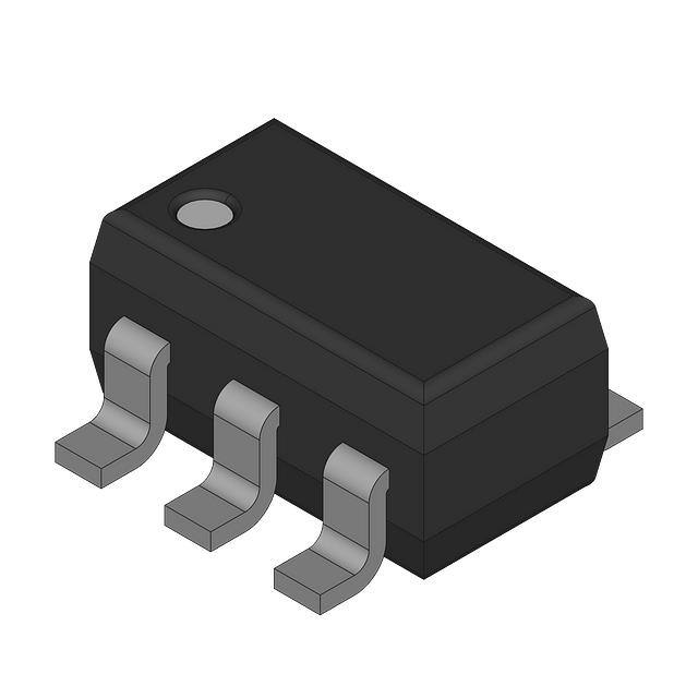
6-Pin SOT23 Package
•
•
•
•
•
•
•
Base Band Converters in Radio
Communication
Motor Current/Bus Voltage Sensors in Digital
Drives
Optical Networking (DWDM, MEMS Based
Switching)
Optical Sensors
Battery Powered Systems
Medical Instrumentations
High-Speed Data Acquisition Systems
High-Speed Closed-Loop Systems
DESCRIPTION
The ADS7884 is a 10-bit, 3-MSPS analog-to-digital converter (ADC), and the ADS7885 is a 8-bit, 3-MSPS ADC.
The devices include a capacitor based SAR A/D converter with inherent sample and hold. The serial interface in
each device is controlled by the CS and SCLK signals for glueless connections with microprocessors and DSPs.
The input signal is sampled with the falling edge of CS, and SCLK is used for conversion and serial data output.
The devices operate from a wide supply range from 2.7 V to 5.5 V. The low power consumption of the devices
make them suitable for battery-powered applications. The devices also include a power saving powerdown
feature for when the devices are operated at lower conversion speeds.
The high level of the digital input to the device is not limited to device VDD. This means the digital input can go as
high as 5.5 V when device supply is 2.7 V. This feature is useful when digital signals are coming from other
circuit with different supply levels. Also this relaxes restriction on power up sequencing.
The ADS7884 and ADS7885 are available in a 6-pin SOT23 package and are specified for operation from –40°C
to 125°C.
Micro-Power Miniature SAR Converter Family
BIT
< 300 KSPS
300 KSPS – 1.25 MSPS
3 MSPS
12-Bit
ADS7866 (1.2 VDD to 3.6 VDD)
ADS7886 (2.35 VDD to 5.25 VDD)
—
10-Bit
ADS7867 (1.2 VDD to 3.6 VDD)
ADS7887 (2.35 VDD to 5.25 VDD)
ADS7884 (2.7 VDD to 5.5 VDD)
8-Bit
ADS7868 (1.2 VDD to 3.6 VDD)
ADS7888 (2.35 VDD to 5.25 VDD)
ADS7885 (2.7 VDD to 5.5 VDD)
1
Please be aware that an important notice concerning availability, standard warranty, and use in critical applications of
Texas Instruments semiconductor products and disclaimers thereto appears at the end of this data sheet.
PRODUCTION DATA information is current as of publication date.
Products conform to specifications per the terms of the Texas
Instruments standard warranty. Production processing does not
necessarily include testing of all parameters.
Copyright © 2008, Texas Instruments Incorporated
�ADS7884
ADS7885
www.ti.com
SLAS567 – MARCH 2008
These devices have limited built-in ESD protection. The leads should be shorted together or the device placed in conductive foam
during storage or handling to prevent electrostatic damage to the MOS gates.
SAR
+IN
OUTPUT
LATCHES
&
3−STATE
DRIVERS
CDAC
SDO
COMPARATOR
VDD
CONVERSION
&
CONTROL
LOGIC
ADS7884/ADS7885
SCLK
CS
PACKAGE/ORDERING INFORMATION (1)
DEVICE
MAXIMUM
INTEGRAL
LINEARITY
(LSB)
MAXIMUM
DIFFERENTIAL
LINEARITY
(LSB)
NO MISSING
CODES AT
RESOLUTION
(BIT)
PACKAGE
TYPE
PACKAGE
DESIGNAT
OR
TEMPERATURE
RANGE
ADS7884
±0.8
±0.8
10
6-Pin
SOT23
DBV
–40°C to 125°C
ADS7885
(1)
±0.4
±0.4
6-Pin
SOT23
8
DBV
PACKAGE
MARKING
ORDERING
INFORMATION
TRANSPORT
MEDIA
QUANTITY
7884
ADS7884SDBVT
Tape and
reel 250
7884
ADS7884SDBVR
Tape and
reel 3000
7885
ADS7885SDBVT
Tape and
reel 250
7885
ADS7885SDBVR
Tape and
reel 3000
–40°C to 125°C
For most current package and ordering information, see the Package Option Addendum at the end of this document, or see the TI
website at www.ti.com.
ABSOLUTE MAXIMUM RATINGS (1)
UNIT
+IN to AGND
–0.3 V to +VDD +0.3 V
+VDD to AGND
–0.3 V to 7.0 V
Digital input voltage to GND
–0.3V to (7.0 V)
Digital output to GND
–0.3 V to (+VDD + 0.3 V)
Operating temperature range
–40°C to 125°C
Storage temperature range
–65°C to 150°C
Junction temperature (TJ Max)
150°C
Power dissipation, SOT23 package
Thermal impedance, θJA
Lead temperature, soldering
(1)
2
(TJ Max–TA)/θJA
SOT23
295.2°C/W
Vapor phase (60 sec)
215°C
Infrared (15 sec)
220°C
Stresses above those listed under absolute maximum ratings may cause permanent damage to the device. Exposure to absolute
maximum conditions for extended periods may affect device reliability.
Submit Documentation Feedback
Copyright © 2008, Texas Instruments Incorporated
Product Folder Link(s): ADS7884 ADS7885
�ADS7884
ADS7885
www.ti.com
SLAS567 – MARCH 2008
ADS7884 SPECIFICATIONS
+VDD = 2.7 V to 5.5 V, TA = –40°C to 125°C, fsample = 2.5 MSPS for VDD = 2.7 V to 3.6 V, fsample = 3 MSPS for VDD = 3.6 V to
5.5 V
PARAMETER
TEST CONDITIONS
MIN
TYP
MAX
UNIT
0
VDD
V
–0.20
VDD+0.20
V
ANALOG INPUT
Full-scale input voltage span (1)
Absolute input voltage range
+IN
(2)
Ci
Input capacitance
IIlkg
Input leakage current
TA = 125°C
27
pF
40
nA
10
Bits
SYSTEM PERFORMANCE
Resolution
No missing codes
10
Bits
INL
Integral nonlinearity
–0.8
±0.3
0.8
LSB (3)
DNL
Differential nonlinearity
–0.8
±0.3
0.8
LSB
EO
Offset error (4) (5) (6)
–1
±0.2
1
LSB
EG
Gain error (5)
–1
±0.2
1
LSB
SAMPLING DYNAMICS
Conversion time
48-MHz SCLK, VDD = 5 V
224
Acquisition time
Maximum throughput rate
240
ns
93.3
48-MHz SCLK, VDD = 5 V
ns
3
Aperture delay
MHz
10
ns
–81
dB
61.7
dB
DYNAMIC CHARACTERISTICS
THD
Total harmonic distortion (7)
100 kHz
SINAD
Signal-to-noise and distortion
100 kHz
SFDR
Spurious free dynamic range
100 kHz
Full power bandwidth
At –3 dB
30
VDD = 2.7 V to 3.6 V
1.5
5.5
VDD = 3.6 V to 5.5 V
2.2
5.5
60
81
dB
MHz
DIGITAL INPUT/OUTPUT
Logic family — CMOS
VIH
High-level input voltage
VIL
Low-level input voltage
VOH
High-level output voltage
At Isource = 200 µA
VOL
Low-level output voltage
At Isink = 200 µA
VDD = 5 V
0.8
VDD = 3 V
0.4
VDD–0.2
0.4
V
V
V
POWER SUPPLY REQUIREMENTS
+VDD
Supply voltage
2.7
At VDD = 3.0 V, 2.5-MSPS throughput
Supply current (normal mode)
Power down state supply current
Power dissipation
(1)
(2)
(3)
(4)
(5)
(6)
(7)
At VDD = 3.0 V, static state
3.3
5.5
2.25
3
1.8
At VDD = 5.0 V, 3-MSPS throughput
3
At VDD = 5.0 V, static state
2
SCLK off
4
1
SCLK on (48 MHz)
90
200
VDD = 5 V, 3 MSPS
15
20
VDD = 3 V, 2.5 MSPS
6.8
V
mA
µA
mW
Ideal input span; does not include gain or offset error.
Refer to Figure 43 for details on sampling circuit
LSB means least significant bit
Measured relative to an ideal full-scale input
Offset error and gain error ensured by characterization.
First transition of 000H to 001H at (Vref/210)
Calculated on the first nine harmonics of the input frequency
Submit Documentation Feedback
Copyright © 2008, Texas Instruments Incorporated
Product Folder Link(s): ADS7884 ADS7885
3
�ADS7884
ADS7885
www.ti.com
SLAS567 – MARCH 2008
ADS7884 SPECIFICATIONS (continued)
+VDD = 2.7 V to 5.5 V, TA = –40°C to 125°C, fsample = 2.5 MSPS for VDD = 2.7 V to 3.6 V, fsample = 3 MSPS for VDD = 3.6 V to
5.5 V
PARAMETER
Power dissipation in static state
TEST CONDITIONS
MIN
TYP
VDD = 5 V
10
VDD = 3 V
5.4
MAX
UNIT
mW
Powerdown time
0.1
µs
Powerup time
0.8
µs
125
°C
TEMPERATURE RANGE
Specified performance
4
–40
Submit Documentation Feedback
Copyright © 2008, Texas Instruments Incorporated
Product Folder Link(s): ADS7884 ADS7885
�ADS7884
ADS7885
www.ti.com
SLAS567 – MARCH 2008
ADS7885 SPECIFICATIONS
+VDD = 2.7 V to 5.5 V, TA = –40°C to 125°C, fsample = 2.5 MSPS for VDD = 2.7 V to 3.6 V, fsample = 3 MSPS for VDD = 3.6 V to
5.5 V
PARAMETER
TEST CONDITIONS
MIN
TYP
MAX
UNIT
0
VDD
V
–0.20
VDD+0.20
V
ANALOG INPUT
Full-scale input voltage span (1)
Absolute input voltage range
+IN
(2)
Ci
Input capacitance
IIlkg
Input leakage current
TA = 125°C
27
pF
40
nA
8
Bits
SYSTEM PERFORMANCE
Resolution
No missing codes
8
Bits
INL
Integral nonlinearity
–0.4
±0.15
0.4
LSB (3)
DNL
Differential nonlinearity
–0.4
±0.1
0.4
LSB
EO
Offset error (4) (5) (6)
–0.4
±0.1
0.4
LSB
EG
Gain error (5)
–0.5
±0.1
0.5
LSB
182
198
SAMPLING DYNAMICS
Conversion time
48-MHz SCLK, VDD = 5 V
Acquisition time
3 MSPS mode
Maximum throughput rate
48-MHz SCLK, VDD = 5 V
ns
135
ns
3
Aperture delay
MHz
10
ns
–68
dB
49.8
dB
DYNAMIC CHARACTERISTICS
THD
Total harmonic distortion (7)
100 kHz
SINAD
Signal-to-noise and distortion
100 kHz
SFDR
Spurious free dynamic range
100 kHz
Full power bandwidth
At –3 dB
30
VDD = 2.7 V to 3.6 V
1.5
5.5
VDD = 3.6 V to 5.5 V
2.2
5.5
49
74
dB
MHz
DIGITAL INPUT/OUTPUT
Logic family — CMOS
VIH
High-level input voltage
VIL
Low-level input voltage
VOH
High-level output voltage
At Isource = 200 µA
VOL
Low-level output voltage
At Isink = 200 µA
VDD = 5 V
0.8
VDD = 3 V
0.4
VDD–0.2
0.4
V
V
V
POWER SUPPLY REQUIREMENTS
+VDD
Supply voltage
2.7
At VDD = 3.0 V, 2.5-MSPS throughput
Supply current (normal mode)
Power down state supply current
Power dissipation
(1)
(2)
(3)
(4)
(5)
(6)
(7)
At VDD = 3.0 V, static state
3.3
5.5
2.25
3
1.8
At VDD = 5.0 V, 3-MSPS throughput
3
At VDD = 5.0 V, static state
2
SCLK off
4
1
SCLK on (48 MHz)
90
200
VDD = 5 V, 3 MSPS
15
20
VDD = 3 V, 2.5 MSPS
6.8
V
mA
µA
mW
Ideal input span; does not include gain or offset error.
Refer to Figure 43 for details on sampling circuit
LSB means least significant bit
Measured relative to an ideal full-scale input
Offset error and gain error ensured by characterization.
First transition of 000H to 001H at (Vref/28)
Calculated on the first nine harmonics of the input frequency
Submit Documentation Feedback
Copyright © 2008, Texas Instruments Incorporated
Product Folder Link(s): ADS7884 ADS7885
5
�ADS7884
ADS7885
www.ti.com
SLAS567 – MARCH 2008
ADS7885 SPECIFICATIONS (continued)
+VDD = 2.7 V to 5.5 V, TA = –40°C to 125°C, fsample = 2.5 MSPS for VDD = 2.7 V to 3.6 V, fsample = 3 MSPS for VDD = 3.6 V to
5.5 V
PARAMETER
TEST CONDITIONS
Power dissipation in static state
MIN
TYP
VDD = 5 V
10
VDD = 3 V
5.4
MAX
UNIT
mW
Powerdown time
0.1
µs
Powerup time
0.8
µs
125
°C
TEMPERATURE RANGE
Specified performance
–40
TIMING REQUIREMENTS (see Figure 1)
All specifications typical at TA = –40°C to 125°C, VDD = 2.7 V to 5.5 V, unless otherwise specified.
TEST CONDITIONS (1)
PARAMETER
ADS7884
tconv
Conversion time
ADS7885
tacq
Aquisition time
tq
Minimum quiet time needed from bus 3-state to start
of next conversion
td1
Delay time, CS low to first data (0) out
tsu1
Setup time, CS low to SCLK low
td2
Delay time, SCLK falling to SDO
th1
Hold time, SCLK falling to data valid (2)
td3
Delay time, 16th SCLK falling edge to SDO 3-state
tw1
Pulse duration, CS
td4
Delay time, CS high to SDO 3-state,
twH
Pulse duration, SCLK high
twL
Pulse duration, SCLK low
Frequency, SCLK
td5
(1)
(2)
6
Delay time, second falling edge of clock and CS to
enter in powerdown (use min spec not to accidently
enter in powerdown) Figure 3
MIN
TYP
MAX
VDD = 3 V
11.5 ×
tSCLK
VDD = 5 V
11.5 ×
tSCLK
VDD = 3 V
9.5 × tSCLK
VDD = 5 V
9.5 × tSCLK
VDD = 3 V
62.5
VDD = 5 V
52
VDD = 3 V
10
VDD = 5 V
10
ns
9
15
VDD = 5 V
8
11
7
VDD = 5 V
5
11
20
VDD = 5 V
9
12
5.5
VDD > 5 V
4
9
15
VDD = 5 V
8
11
10
VDD = 5 V
10
9
15
VDD = 5 V
8
11
0.45 × tSCLK
VDD = 5 V
0.45 × tSCLK
VDD = 3 V
0.45 × tSCLK
VDD = 5 V
0.45 × tSCLK
ns
ns
VDD = 3 V
VDD = 3 V
ns
ns
VDD = 3 V
VDD = 3 V
ns
ns
VDD = 3 V
VDD < 3 V
ns
ns
VDD = 3 V
VDD = 3 V
UNIT
ns
ns
ns
VDD = 3 V
40
VDD = 5 V
48
VDD = 3 V
–2
4
VDD = 5 V
–2
3
MHz
ns
3-V Specifications apply from 2.7 V to 3.6 V, and 5-V specifications apply from 4.5 V to 5.5 V.
With 10-pf load.
Submit Documentation Feedback
Copyright © 2008, Texas Instruments Incorporated
Product Folder Link(s): ADS7884 ADS7885
�ADS7884
ADS7885
www.ti.com
SLAS567 – MARCH 2008
TIMING REQUIREMENTS (see Figure 1) (continued)
All specifications typical at TA = –40°C to 125°C, VDD = 2.7 V to 5.5 V, unless otherwise specified.
TEST CONDITIONS (1)
PARAMETER
Delay time, CS and 10th falling edge of clock to
enter in powerdown (use max spec not to accidently
enter in powerdown) Figure 3
td6
MIN
TYP
MAX
VDD = 3 V
–2
4
VDD = 5 V
–2
3
UNIT
ns
DEVICE INFORMATION
SOT23 PACKAGE
(TOP VIEW)
VDD
1
6
CS
GND
2
5
SDO
VIN
3
4
SCLK
TERMINAL FUNCTIONS
TERMINAL
NAME
NO.
I/O
DESCRIPTION
VDD
1
–
Power supply input also acts like a reference voltage to ADC.
GND
2
–
Ground for power supply, all analog and digital signals are referred with respect to this pin.
VIN
3
I
Analog signal input
SCLK
4
I
Serial clock
SDO
5
O
Serial data out
CS
6
I
Chip select signal, active low
ADS7884 NORMAL OPERATION
The cycle begins with the falling edge of CS. This point is indicated as a in Figure 1. With the falling edge of CS,
the input signal is sampled and the conversion process is initiated. The device outputs data while the conversion
is in progress. The data word contains 2 leading zeros, followed by 10-bit data in MSB first format and padded by
4 lagging zeros.
The falling edge of CS clocks out the first zero, and a second zero is clocked out on FIRST falling edge of the
clock. Data is in MSB first format with the MSB being clocked out on the 2nd falling edge. Data is padded with
four lagging zeros as shown in Figure 1. The conversion ends on the first rising edge of SCLK after the 11th
falling edge. At this point the device enters the acquisition phase. This point is indicated by b in Figure 1.
Figure 1 shows device data is read in a sixteen clock frame. However, CS can be asserted (pulled high) any time
after 11 clocks have elapsed. SDO goes to 3-state with the CS high level. The next conversion should not be
started (by pulling CS low) until the end of the quiet sampling time (tq) after SDO goes to 3-state or until the
minimum acquisition time (tacq) has elapsed. To continue normal operation, it is necessary that CS is not pulled
high until point b. Without this, the device does not enter the acquisition phase and no valid data is available in
the next cycle. (Also refer to the Powerdown Mode section for more details.) CS going high any time after the
conversion start aborts the ongoing conversion and SDO goes to 3-state.
The high level of the digital input to the device is not limited to device VDD. This means the digital input can go as
high as 5.5 V when the device supply is 2.7 V. This feature is useful when digital signals are coming from
another circuit with different supply levels. Also, this relaxes the restriction on powerup sequencing. However, the
digital output levels (VOH and VOL) are governed by VDD as listed in the Specifications table.
Submit Documentation Feedback
Copyright © 2008, Texas Instruments Incorporated
Product Folder Link(s): ADS7884 ADS7885
7
�ADS7884
ADS7885
www.ti.com
SLAS567 – MARCH 2008
a
tconv
tw1
tacq
a
b
CS
tsu1
1
SCLK
2
11
3
th1
td2
td1
SDO
0
0
15
14
16
td4
D8
D9
13
12
td3
0
0
D0
0
0
tq
Figure 1. ADS7884 Interface Timing Diagram
ADS7885 NORMAL OPERATION
The cycle begins with the falling edge of CS . This point is indicated as a in Figure 2. With the falling edge of CS,
the input signal is sampled and the conversion process is initiated. The device outputs data while the conversion
is in progress. The data word contains 2 leading zeros, followed by 8-bit data in MSB first format and padded by
6 lagging zeros.
The falling edge of CS clocks out the first zero, and a second zero is clocked out on FIRST falling edge of the
clock. Data is in MSB first format with the MSB being clocked out on the 3rd falling edge. Data is padded with six
lagging zeros as shown in Figure 2. On the 16th falling edge of SCLK, SDO goes to the 3-state condition. The
conversion ends on the first rising edge of SCLK after the 9th falling edge. At this point the device enters the
acquisition phase. This point is indicated by b in Figure 2.
Figure 2 shows device data is read in a sixteen clock frame. However, CS can be asserted (pulled high) any time
after 9 clocks have elapsed (after the 10th falling edge of SCLK). SDO goes to 3-state with the CS high level.
The next conversion should not be started (by pulling CS low) until the end of the quiet sampling time (tq) after
SDO goes to 3-state or until the minimum acquisition time (tacq) has elapsed. To continue normal operation, it is
necessary that CS is not pulled high until point b. Without this, the device does not enter the acquisition phase
and no valid data is available in the next cycle. (Also refer to the Powerdown Mode section for more details.) CS
going high any time after the conversion start aborts the ongoing conversion and SDO goes to 3-state.
The high level of the digital input to the device is not limited to device VDD. This means the digital input can go as
high as 5.5 V when the device supply is 2.7 V. This feature is useful when digital signals are coming from
another circuit with different supply levels. Also, this relaxes the restriction on powerup sequencing. However, the
digital output levels (VOH and VOL) are governed by VDD as listed in the Specifications section.
a
tconv
tw1
tacq
a
b
CS
tsu1
1
SCLK
0
9
3
th1
td2
td1
SDO
2
0
D7
D6
11
10
15
14
16
td4
td3
D0
0
0
0
0
0
tq
Figure 2. ADS7885 Interface Timing Diagram
POWER DOWN MODE
The device enters powerdown mode if CS goes high anytime after the 2nd SCLK falling edge to before the 10th
SCLK falling edge. Ongoing conversion stops and SDO goes to 3-state under this powerdown condition as
shown in Figure 3.
8
Submit Documentation Feedback
Copyright © 2008, Texas Instruments Incorporated
Product Folder Link(s): ADS7884 ADS7885
�ADS7884
ADS7885
www.ti.com
SLAS567 – MARCH 2008
td6
td5
CS
1
2
3
4
5
9
10
16
SCLK
SDO
Figure 3. Entering Power Down Mode
A dummy cycle with CS low for more than 10 SCLK falling edges brings the device out of powerdown mode. For
the device to come to the fully powered up condition it takes 0.8 µs. CS can be pulled high any time after the
10th falling edge as shown in Figure 4. Note that the powerup time of 0.8 µsec is more than a single conversion
cycle at 3 MSPS speed. This means the device requires three dummy conversion frames at 3 MSPS speed or
one elongated dummy conversion frame. The data during dummy conversion frames is invalid.
Device Starts
Powering Up
Device Fully
Powered-Up
CS
SCLK
1
SDO
2
3
4
5
6
7
8
9 10 11 12 13 14 15
16
1
2
3
4
5
6
Invalid Data
7
8
9
10 11 12 13 14 15 16
Valid Data
Figure 4. Exiting Power Down Mode
Submit Documentation Feedback
Copyright © 2008, Texas Instruments Incorporated
Product Folder Link(s): ADS7884 ADS7885
9
�ADS7884
ADS7885
www.ti.com
SLAS567 – MARCH 2008
TYPICAL CHARACTERISTICS ADS7884
SUPPLY CURRENT
vs
SUPPLY VOLTAGE
SUPPLY CURRENT
vs
SCLK FREQUENCY
3.5
3.2
TA = 25°C,
fs = 3MSPS at VDD = 5 V,
fs = 2.5 MSPS at VDD = 3 V
2.5 MSPS
2.4
2.2
2.5
5V
ICC - Supply Current - mA
2.6
2.5
2
3V
1.5
1
5.5
0
3V
10
20
30
40
fSCLK - Frequency - MHz
50
100
200 300 400 500
fs - Sample Rate - KSPS
600
700
Figure 6.
Figure 7.
INPUT LEAKAGE CURRENT
vs
FREE-AIR TEMPERATURE
SIGNAL-TO-NOISE RATIO
vs
INPUT FREQUENCY
SIGNAL-TO-NOISE + DISTORTION
vs
INPUT FREQUENCY
62
62
TA = 25°C,
fs = 3 MSPS,
VDD = 5 V
61.9
10
Signal-to-Noise Ratio - dB
20
5V
0
-10
0V
-20
61.8
61.9
SNR 5 V
Signal-to-Noise + Distortion - dB
VDD = 5 V
61.7
61.6
61.5
61.4
61.3
61.2
-30
61.1
-40
-40 -20
0
20
40 60 80 100 120
TA - Free-Air Temperature - °C
61.8
TA = 25°C,
fs = 3 MSPS,
VDD = 5 V
61.7
SINAD 5 V
61.6
61.5
61.4
61.3
61.2
61.1
61
0
200
400
600
800
fi - Input Frequency - KHz
61
0
1000
200
400
600
800
fi - Input Frequency - KHz
1000
Figure 8.
Figure 9.
Figure 10.
SIGNAL-TO-NOISE + DISTORTION
vs
SUPPLY VOLTAGE
SIGNAL-TO-NOISE + DISTORTION
vs
FREE-AIR TEMPERATURE
DIFFERENTIAL NONLINEARITY
vs
FREE-AIR TEMPERATURE
TA = 25°C,
fs = 3 MSPS or 2.5 MSPS
2.5 MSPS
61.8
61.7
3 MSPS
61.6
61.5
61.4
61.3
61.2
61.1
61
2.7
3.4
4.1
4.8
VDD - Supply Voltage - V
5.5
Figure 11.
0.8
62
61.9
VDD = 5 V at 3 MSPS,
VDD = 3 V at 2.5 MSPS
3V, 2.5MSPS
61.8
61.7
61.6
5V, 3 MSPS
61.5
61.4
61.3
61.2
61.1
61
-40
-20
0
20 40 60
80 100 120
TA - Free-Air Temperature - °C
Figure 12.
Submit Documentation Feedback
DNL - Differential Nonlinearity - LSBs
62
61.9
SINAD - Signal-to-Noise and Distortion - dB
SINAD - Signal-to-Noise and Distortion - dB
1
Figure 5.
30
10
5V
1.5
0
0
0
3.4
4.1
4.8
VDD - Supply Voltage - V
2
0.5
0.5
2
2.7
TA = 25°C,
SCLK = 48 MHz at VDD = 5 V,
SCLK = 40 MHz at VDD = 3 V,
Power Down,
SCLK = Free Running
3
3 MSPS
2.8
3
TA = 25°C
ICC - Supply Current - mA
ICC - Supply Current - mA
3
Input Leakage Current - nA
SUPPLY CURRENT
vs
SAMPLE RATE
TA = 25°C
0.6 VDD = 5 V at 3 MSPS,
VDD = 3 V at 2.5 MSPS
MAXDNL, 5 V, 3MSPS
0.4
0.2
MAXDNL, 3 V, 2.5 MSPS
0
MINDNL, 3 V, 2.5 MSPS
-0.2
-0.4
MINDNL, 5 V, 3MSPS
-0.6
-0.8
-40
-20
0
20
40
60
80
100 120
TA - Free-Air Temperature - °C
Figure 13.
Copyright © 2008, Texas Instruments Incorporated
Product Folder Link(s): ADS7884 ADS7885
�ADS7884
ADS7885
www.ti.com
SLAS567 – MARCH 2008
TYPICAL CHARACTERISTICS ADS7884 (continued)
INTEGRAL NONLINEARITY
vs
FREE-AIR TEMPERATURE
MAXINL, 5 V, 3MSPS
0.2
MAXINL, 3 V, 2.5 MSPS
0
MININL, 5 V, 3MSPS
-0.2
MININL, 3 V, 2.5 MSPS
-0.4
-0.6
-0.8
-40
0.8
0.6
MAXDNL, 3MSPS
0.4
0.2
0
MAXDNL, 2.5 MSPS
MINDNL, 2.5 MSPS
-0.2
-0.4
MINDNL, 3MSPS
-0.6
-0.8
2.7
-20
0
20 40 60 80 100 120
TA - Free-Air Temperature - °C
TA = 25°C
TA = 25°C
INL - Integral Nonlinearity - LSBs
0.4
INTEGRAL NONLINEARITY
vs
SUPPLY VOLTAGE
0.8
TA = 25°C
VDD = 5 V at 3 MSPS,
VDD = 3 V at 2.5 MSPS
0.6
DNL - Differential Nonlinearity - LSBs
INL - Integral Nonlinearity - LSBs
0.8
DIFFERENTIAL NONLINEARITY
vs
SUPPLY VOLTAGE
3.4
4.1
4.8
VDD - Supply Voltage - V
MAXINL, 2.5 MSPS
MININL, 2.5 MSPS
-0.2
MININL, 3MSPS
-0.4
-0.6
3.4
4.1
4.8
Figure 16.
OFFSET ERROR
vs
SUPPLY VOLTAGE
OFFSET ERROR
vs
FREE-AIR TEMPERATURE
GAIN ERROR
vs
SUPPLY VOLTAGE
0.5
0.5
0.4
0.4
0.3
3 V, 2.5 MSPS
3 MSPS
0
TA = 25°C,
fs = 3 MSPS or 2.5 MSPS,
VDD = 5 V at 3 MSPS,
VDD = 3 V at 2.5 MSPS
3.4
4.1
4.8
VDD - Supply Voltage - V
0.2
0.1
0
5 V, 3MSPS
-0.1
-0.2
fs = 3 MSPS or 2.5 MSPS,
VDD = 5 V at 3 MSPS,
VDD = 3 V at 2.5 MSPS
-0.3
-0.4
-0.5
-40
5.5
Gain Error - LSBs
Offset Error - LSBs
2.5 MSPS
-20
0
20
40
60
80
100
0.2
TA = 25°C,
fs = 3 MSPS or 2.5 MSPS,
VDD = 5 V at 3 MSPS,
VDD = 3 V at 2.5 MSPS
0.1
2.5 MSPS
0
-0.1
3 MSPS
-0.2
-0.3
-0.4
120
TA - Free-Air Temperature - °C
Figure 17.
5.5
VDD - Supply Voltage - V
0.3
Offset Error - LSBs
0
-0.8
2.7
5.5
MAXINL, 3MSPS
0.2
Figure 15.
0.25
-0.5
2.7
0.4
Figure 14.
0.5
-0.25
0.6
Figure 18.
-0.5
2.7
3.4
4.1
4.8
VDD - Supply Voltage - V
5.5
Figure 19.
GAIN ERROR
vs
FREE-AIR TEMPERATURE
0.2
0.15
Gain Error - LSBs
0.1
fs = 3 MSPS or 2.5 MSPS,
VDD = 5 V at 3 MSPS,
VDD = 3 V at 2.5 MSPS
0.05
3 V, 2.5 MSPS
0
-0.05
-0.1
5 V, 3 MSPS
-0.15
-0.2
-40 -20
0
20 40 60
80 100 120
TA - Free-Air Temperature - °C
Figure 20.
Submit Documentation Feedback
Copyright © 2008, Texas Instruments Incorporated
Product Folder Link(s): ADS7884 ADS7885
11
�ADS7884
ADS7885
www.ti.com
SLAS567 – MARCH 2008
TYPICAL CHARACTERISTICS ADS7884 (continued)
DNL
0.8
VDD = 5 V,
fs = 3 MSPS,
TA = 25°C
0.6
DNL - LSBs
0.4
0.2
0
-0.2
-0.4
-0.6
-0.8
0
256
512
Output Code
768
1024
768
1024
Figure 21.
INL
0.8
VDD = 5 V,
fs = 3 MSPS,
TA = 25°C
0.6
INL - LSBs
0.4
0.2
0
-0.2
-0.4
-0.6
-0.8
0
256
512
Output Code
Figure 22.
FFT
0
-40
fs = 3 MSPS,
fin - 100 kHz,
VDD = 5 V,
-60
16384 N Points
power - dB
-20
-80
-100
-120
-140
0
12
250
500
750
f - Frequency - kHz
Figure 23.
1000
Submit Documentation Feedback
1250
1500
Copyright © 2008, Texas Instruments Incorporated
Product Folder Link(s): ADS7884 ADS7885
�ADS7884
ADS7885
www.ti.com
SLAS567 – MARCH 2008
TYPICAL CHARACTERISTICS ADS7885
SUPPLY CURRENT
vs
SUPPLY VOLTAGE
SUPPLY CURRENT
vs
SCLK FREQUENCY
3
3
2.8
TA = 25°C,
fs = 3 MSPS at VDD = 5 V,
fs = 2.5 MSPS at VDD = 3 V
TA = 25°C
3 MSPS
2.5
2.4
2.3
2.5 MSPS
2.2
2.5
ICC - Supply Current - mA
2.6
TA = 25°C,
SCLK = 48 MHz at VDD = 5 V,
SCLK = 40 MHz at VDD = 3 V,
Power Down,
SCLK = Free Running
5V
2.5
ICC - Supply Current - mA
2.7
ICC - Supply Current - mA
SUPPLY CURRENT
vs
SAMPLE RATE
2
3V
1.5
1
2
5V
1.5
3V
1
0.5
0.5
2.1
2
2.7
3.4
4.1
4.8
0
0
0
5.5
10
20
30
40
fSCLK - Frequency - MHz
VDD - Supply Voltage - V
200 300 400 500 600
fs - Sample Rate - KSPS
700
Figure 26.
INPUT LEAKAGE CURRENT
vs
FREE-AIR TEMPERATURE
SIGNAL-TO-NOISE RATIO
vs
INPUT FREQUENCY
SIGNAL-TO-NOISE + DISTORTION
vs
INPUT FREQUENCY
51
51
TA = 25°C,
fs = 3 MSPS,
VDD = 5 V
5V
Signal-to-Noise Ratio - dB
50.6
10
0
-10
-20
0V
-30
50.4
50.2
50
SNR 5 V
49.8
49.6
49.4
49.2
50.6
50.4
50.2
50
49.8
SINAD 5 V
49.6
49.4
49.2
49
0
-20
0
20 40 60 80 100 120
TA - Free-Air Temperature - °C
TA = 25°C,
fs = 3 MSPS,
VDD = 5 V
50.8
Signal-to-Noise + Distortion - dB
50.8
20
200
400
600
800
fi - Input Frequency - KHz
49
0
1000
200
400
600
800
fi - Input Frequency - KHz
1000
Figure 27.
Figure 28.
Figure 29.
SIGNAL-TO-NOISE + DISTORTION
vs
SUPPLY VOLTAGE
SIGNAL-TO-NOISE + DISTORTION
vs
FREE-AIR TEMPERATURE
DIFFERENTIAL NONLINEARITY
vs
FREE-AIR TEMPERATURE
SINAD - Signal-to-Noise and Distortion - dB
51
50.8
TA = 25°C,
fs = 3 MSPS or 2.5 MSPS
50.6
50.4
50.2
3 MSPS
50
49.8
2.5 MSPS
49.6
49.4
49.2
49
2.7
3.4
4.1
4.8
5.5
VDD - Supply Voltage - V
Figure 30.
51
50.8
0.4
VDD = 5 V at 3 MSPS,
VDD = 3 V at 2.5 MSPS
DNL - Differential Nonlinearity - LSBs
Input Leakage Current - nA
100
Figure 25.
VDD = 5 V
-40
-40
0
Figure 24.
30
SINAD - Signal-to-Noise and Distortion - dB
50
50.6
50.4
50.2
5 V, 3 MSPS
50
49.8
49.6
3 V, 2.5MSPS
49.4
49.2
49
-40
-20
0
20 40 60
80 100
TA - Free-Air Temperature - °C
120
Figure 31.
TA = 25°C
VDD = 5 V at 3 MSPS,
VDD = 3 V at 2.5 MSPS
0.3
0.2
MAXDNL, 5 V, 3 MSPS
0.1
0
MINDNL, 5 V, 3 MSPS
MAXDNL, 3 V, 2.5 MSPS
-0.1
MINDNL, 3 V, 2.5 MSPS
-0.2
-0.3
-0.4
-40
-20
0
20
40 60
80 100 120
TA - Free-Air Temperature - °C
Figure 32.
Submit Documentation Feedback
Copyright © 2008, Texas Instruments Incorporated
Product Folder Link(s): ADS7884 ADS7885
13
�ADS7884
ADS7885
www.ti.com
SLAS567 – MARCH 2008
TYPICAL CHARACTERISTICS ADS7885 (continued)
INTEGRAL NONLINEARITY
vs
FREE-AIR TEMPERATURE
DIFFERENTIAL NONLINEARITY
vs
SUPPLY VOLTAGE
MAXINL, 5 V, 3 MSPS MAXINL, 3 V, 2.5 MSPS
0.1
MININL, 3 V, 2.5 MSPS
0
-0.1
MININL, 5 V, 3 MSPS
-0.2
-0.3
-0.4
-40
-20
0
20
40
60
80
0.3
0.2
MAXDNL, 2.5 MSPS
MAXDNL, 3 MSPS
0.1
0
-0.1
-0.2
-0.3
-0.4
2.7
100 120
0.2
0
-0.1
MININL, 3 MSPS
MININL, 2.5 MSPS
-0.2
-0.3
-0.4
2.7
5.5
MAXINL, 3 MSPS
MAXINL, 2.5 MSPS
0.1
3.4
4.1
4.8
Figure 35.
OFFSET ERROR
vs
SUPPLY VOLTAGE
OFFSET ERROR
vs
FREE-AIR TEMPERATURE
GAIN ERROR
vs
SUPPLY VOLTAGE
0.4
0.4
0.3
0.2
2.5 MSPS
0
3 MSPS
-0.1
-0.2
-0.3
3.4
4.1
4.8
VDD - Supply Voltage - V
0.3
0.2
0.1
3V, 2.5 MSPS
0
5V, 3 MSPS
-0.1
0.1
-0.2
-0.3
-0.3
Figure 36.
-20 0
20 40 60
80 100 120
TA - Free-Air Temperature - °C
Figure 37.
TA = 25°C,
fs = 3 MSPS or 2.5 MSPS,
VDD = 5 V at 3 MSPS,
VDD = 3 V at 2.5 MSPS
2.5 MSPS
0
-0.1
-0.2
-0.4
-40
5.5
fs = 3 MSPS or 2.5 MSPS,
VDD = 5 V at 3 MSPS,
VDD = 3 V at 2.5 MSPS
Gain Error - LSBs
TA = 25°C,
fs = 3 MSPS or 2.5 MSPS,
VDD = 5 V at 3 MSPS,
VDD = 3 V at 2.5 MSPS
5.5
VDD - Supply Voltage - V
Figure 34.
Offset Error - LSBs
Offset Error - LSBs
3.4
4.1
4.8
VDD - Supply Voltage - V
0.3
Figure 33.
0.4
-0.4
2.7
MINDNL, 3 MSPS
MINDNL, 2.5 MSPS
TA - Free-Air Temperature - °C
0.1
INL - Integral Nonlinearity - LSBs
0.2
TA = 25°C
TA = 25°C
DNL - Differential Nonlinearity - LSBs
INL - Integral Nonlinearity - LSBs
TA = 25°C
VDD = 5 V at 3 MSPS,
VDD = 3 V at 2.5 MSPS
0.3
0.2
0.4
0.4
0.4
0.3
INTEGRAL NONLINEARITY
vs
SUPPLY VOLTAGE
-0.4
2.7
3 MSPS
3.4
4.1
4.8
VDD - Supply Voltage - V
5.5
Figure 38.
GAIN ERROR
vs
FREE-AIR TEMPERATURE
0.2
0.15
Gain Error - LSBs
0.1
0.05
fs = 3 MSPS or 2.5 MSPS,
VDD = 5 V at 3 MSPS,
VDD = 3 V at 2.5 MSPS
3V, 2.5 MSPS
0
5V, 3 MSPS
-0.05
-0.1
-0.15
-0.2
-40
-20
0
20 40 60
80 100
TA - Free-Air Temperature - °C
120
Figure 39.
14
Submit Documentation Feedback
Copyright © 2008, Texas Instruments Incorporated
Product Folder Link(s): ADS7884 ADS7885
�ADS7884
ADS7885
www.ti.com
SLAS567 – MARCH 2008
TYPICAL CHARACTERISTICS ADS7885 (continued)
DNL
0.4
VDD = 5 V,
fs = 3 MSPS,
TA = 25°C
DNL - LSBs
0.3
0.2
0.1
0
-0.1
-0.2
-0.3
-0.4
0
64
128
Output Code
192
256
192
256
Figure 40.
INL
0.4
VDD = 5 V,
fs = 3 MSPS,
TA = 25°C
INL - LSBs
0.3
0.2
0.1
0
-0.1
-0.2
-0.3
-0.4
0
64
128
Output Code
Figure 41.
FFT
0
fs = 3 MSPS,
fin - 100 kHz,
VDD = 5 V,
Power - dB
-20
-40
16384 N Points
-60
-80
-100
-120
0
250
500
750
1000
1250
1500
F - Frequency - kHz
Figure 42.
Submit Documentation Feedback
Copyright © 2008, Texas Instruments Incorporated
Product Folder Link(s): ADS7884 ADS7885
15
�ADS7884
ADS7885
www.ti.com
SLAS567 – MARCH 2008
APPLICATION INFORMATION
VDD
20 W
50 W
IN
20 pF
50 W
7 pF
GND
Figure 43. Typical Equivalent Sampling Circuit
Driving the VIN and VDD Pins of the ADS7884 and ADS7885
The VIN input to the ADS7884 and ADS7885 should be driven with a low impedance source. In most cases
additional buffers are not required. In cases where the source impedance exceeds 200 Ω, using a buffer would
help achieve the rated performance of the converter. The THS4031 is a good choice for the driver amplifier
buffer.
The reference voltage for the ADS7884 and ADS7885 A/D converters are derived from the supply voltage
internally. The devices offer limited low-pass filtering functionality on-chip. The supply to these converters should
be driven with a low impedance source and should be decoupled to the ground. A 1-µF storage capacitor and a
10-nF decoupling capacitor should be placed close to the device. Wide, low impedance traces should be used to
connect the capacitor to the pins of the device. The ADS7884 and ADS7885 draw very little current from the
supply lines. The supply line can be driven by either:
• Directly from the system supply.
• A reference output from a low drift and low drop out reference voltage generator like REF3030 or REF3130.
The ADS7884 and ADS7885 can operate off a wide range of supply voltages. The actual choice of the
reference voltage generator would depend upon the system. Figure 45 shows one possible application circuit.
• A low-pass filtered version of the system supply followed by a buffer like the zero-drift OPA735 can also be
used in cases where the system power supply is noisy. Care should be taken to ensure that the voltage at the
VDD input does not exceed 7 V (especially during power up) to avoid damage to the converter. This can be
done easily using single supply CMOS amplifiers like the OPA735. Figure 46 shows one possible application
circuit.
VDD
1 mF
VDD
CS
VIN
SDO
GND
SCLK
10 nF
Figure 44. Supply/Reference Decoupling Capacitors
5V
REF3030
IN
1 mF
3V
OUT
VDD
CS
VIN
SDO
GND
SCLK
GND
1 mF
10 nF
Figure 45. Using the REF3030 Reference
16
Submit Documentation Feedback
Copyright © 2008, Texas Instruments Incorporated
Product Folder Link(s): ADS7884 ADS7885
�ADS7884
ADS7885
www.ti.com
SLAS567 – MARCH 2008
5V
C1
R1
10 W
7V
_
R2
VDD
CS
VIN
SDO
GND
SCLK
+
1 mF
1 mF
10 nF
Figure 46. Buffering with the OPA735
Submit Documentation Feedback
Copyright © 2008, Texas Instruments Incorporated
Product Folder Link(s): ADS7884 ADS7885
17
�PACKAGE OPTION ADDENDUM
www.ti.com
10-Dec-2020
PACKAGING INFORMATION
Orderable Device
Status
(1)
Package Type Package Pins Package
Drawing
Qty
Eco Plan
(2)
Lead finish/
Ball material
MSL Peak Temp
Op Temp (°C)
Device Marking
(3)
(4/5)
(6)
ADS7884SDBVR
ACTIVE
SOT-23
DBV
6
3000
RoHS & Green
SN
Level-2-260C-1 YEAR
-40 to 125
7884
ADS7884SDBVT
ACTIVE
SOT-23
DBV
6
250
RoHS & Green
SN
Level-2-260C-1 YEAR
-40 to 125
7884
ADS7885SDBVR
ACTIVE
SOT-23
DBV
6
3000
RoHS & Green
SN
Level-2-260C-1 YEAR
-40 to 125
7885
ADS7885SDBVT
ACTIVE
SOT-23
DBV
6
250
RoHS & Green
SN
Level-2-260C-1 YEAR
-40 to 125
7885
(1)
The marketing status values are defined as follows:
ACTIVE: Product device recommended for new designs.
LIFEBUY: TI has announced that the device will be discontinued, and a lifetime-buy period is in effect.
NRND: Not recommended for new designs. Device is in production to support existing customers, but TI does not recommend using this part in a new design.
PREVIEW: Device has been announced but is not in production. Samples may or may not be available.
OBSOLETE: TI has discontinued the production of the device.
(2)
RoHS: TI defines "RoHS" to mean semiconductor products that are compliant with the current EU RoHS requirements for all 10 RoHS substances, including the requirement that RoHS substance
do not exceed 0.1% by weight in homogeneous materials. Where designed to be soldered at high temperatures, "RoHS" products are suitable for use in specified lead-free processes. TI may
reference these types of products as "Pb-Free".
RoHS Exempt: TI defines "RoHS Exempt" to mean products that contain lead but are compliant with EU RoHS pursuant to a specific EU RoHS exemption.
Green: TI defines "Green" to mean the content of Chlorine (Cl) and Bromine (Br) based flame retardants meet JS709B low halogen requirements of