Sample &
Buy
Product
Folder
Support &
Community
Tools &
Software
Technical
Documents
ADS7887, ADS7888
SLAS468A – JUNE 2005 – REVISED AUGUST 2016
ADS788x 10-Bit, 8-Bit, 1.25-MSPS, Micro-Power,
Miniature SAR Analog-to-Digital Converters
1 Features
3 Description
•
•
•
•
•
•
•
The ADS7887 device is a 10-bit, 1.25-MSPS, analogto-digital converter (ADC), and the ADS7888 device
is a 8-bit, 1.25-MSPS ADC. These devices include a
capacitor-based SAR A/D converter with inherent
sample and hold. The serial interface in each device
is controlled by the CS and SCLK signals for glueless
connections with microprocessors and DSPs. The
input signal is sampled with the falling edge of CS,
and SCLK is used for conversion and serial data
output.
1
•
•
•
•
•
•
•
•
1.25-MHz Sample Rate Serial Device
10-Bit Resolution (ADS7887)
8-Bit Resolution (ADS7888)
Zero Latency
25-MHz Serial Interface
Supply Range: 2.35 V to 5.25 V
Typical Power Dissipation at 1.25 MSPS:
– 3.8 mW at 3-V VDD
– 8 mw at 5-V VDD
±0.35 LSB INL, DNL (ADS7887)
±0.15 LSB INL, ±0.1 LSB DNL (ADS7888)
61 dB SINAD, –84 dB THD (ADS7887)
49.5 dB SINAD, –67.5 dB THD (ADS7888)
Unipolar Input Range: 0 V to VDD
Power-Down Current: 1 µA
Wide Input Bandwidth: 15 MHz at 3 dB
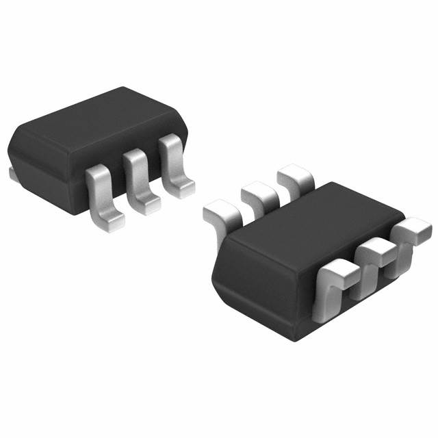
6-Pin SOT23 and SC70 Packages
The devices operate from a wide supply range from
2.35 V to 5.25 V. The low power consumption of the
devices make them suitable for battery-powered
applications. The devices also include a powersaving, power-down feature for when the devices are
operated at lower conversion speeds.
The high level of the digital input to the device is not
limited to device VDD. This means the digital input can
go as high as 5.25 V when device supply is 2.35 V.
This feature is useful when digital signals are coming
from other circuit with different supply levels. Also this
relaxes restriction on power-up sequencing.
2 Applications
•
•
•
•
•
•
•
•
Base Band Converters in Radio Communication
Motor Current and Bus Voltage Sensors in Digital
Drives
Optical Networking (DWDM, MEMS-Based
Switching)
Optical Sensors
Battery-Powered Systems
Medical Instrumentations
High-Speed Data Acquisition Systems
High-Speed Closed-Loop Systems
The ADS7887 and ADS7888 are available in 6-pin
SOT-23 and SC70 packages and are specified for
operation from –40°C to 125°C.
Device Information(1)
PART NUMBER
ADS7887
ADS7888
PACKAGE
BODY SIZE (NOM)
SOT-23 (6)
2.90 mm × 1.60 mm
SC70 (6)
2.00 mm × 1.25 mm
(1) For all available packages, see the orderable addendum at
the end of the data sheet.
Functional Block Diagram
SAR
+IN
CDAC
OUTPUT
LATCHES
AND
3−STATE
DRIVERS
SDO
COMPARATOR
VDD
ADS7887/ADS7888
CONVERSION
AND
CONTROL
LOGIC
SCLK
CS
Copyright © 2016, Texas Instruments Incorporated
1
An IMPORTANT NOTICE at the end of this data sheet addresses availability, warranty, changes, use in safety-critical applications,
intellectual property matters and other important disclaimers. PRODUCTION DATA.
�ADS7887, ADS7888
SLAS468A – JUNE 2005 – REVISED AUGUST 2016
www.ti.com
Table of Contents
1
2
3
4
5
6
7
8
Features ..................................................................
Applications ...........................................................
Description .............................................................
Revision History.....................................................
Companion Products.............................................
Device Comparison ...............................................
Pin Configuration and Functions .........................
Specifications.........................................................
8.1
8.2
8.3
8.4
8.5
8.6
8.7
8.8
9
1
1
1
2
3
4
5
6
Absolute Maximum Ratings ...................................... 6
ESD Ratings.............................................................. 6
Recommended Operating Conditions....................... 6
Thermal Information .................................................. 6
Electrical Characteristics – ADS7887 ....................... 7
Electrical Characteristics – ADS7888 ....................... 8
Timing Requirements ................................................ 9
Typical Characteristics ............................................ 10
Detailed Description ............................................ 16
9.1 Overview ................................................................ 16
9.2 Functional Block Diagram ....................................... 16
9.3 Feature Description................................................. 17
9.4 Device Functional Modes........................................ 18
10 Application and Implementation........................ 20
10.1 Application Information.......................................... 20
10.2 Typical Application ................................................ 20
11 Power Supply Recommendations ..................... 22
12 Layout................................................................... 23
12.1 Layout Guidelines ................................................. 23
12.2 Layout Example .................................................... 23
13 Device and Documentation Support ................. 24
13.1
13.2
13.3
13.4
13.5
13.6
13.7
Documentation Support ........................................
Related Links ........................................................
Receiving Notification of Documentation Updates
Community Resources..........................................
Trademarks ...........................................................
Electrostatic Discharge Caution ............................
Glossary ................................................................
24
24
24
24
24
24
24
14 Mechanical, Packaging, and Orderable
Information ........................................................... 25
4 Revision History
NOTE: Page numbers for previous revisions may differ from page numbers in the current version.
Changes from Original (June 2005) to Revision A
Page
•
Added ESD Ratings table, Feature Description section, Device Functional Modes, Application and Implementation
section, Power Supply Recommendations section, Layout section, Device and Documentation Support section, and
Mechanical, Packaging, and Orderable Information section .................................................................................................. 1
•
Changed Thermal Information table ....................................................................................................................................... 6
2
Submit Documentation Feedback
Copyright © 2005–2016, Texas Instruments Incorporated
Product Folder Links: ADS7887 ADS7888
�ADS7887, ADS7888
www.ti.com
SLAS468A – JUNE 2005 – REVISED AUGUST 2016
5 Companion Products
PART NUMBER
SN74LVTH245A
LMV761
TPS54418
NAME
3.3-V ABT Octal Bus Transceivers With 3-State Outputs
Low Voltage, Precision Comparator with Push-Pull Output
2.95V to 6V Input, 4A Synchronous Step-Down SWIFT™ Converter
LMV339
Quad General Purpose Low-Voltage Comparators
TPS730
Low-Noise, High PSRR, RF 200-mA Low-Dropout Linear Regulators
Copyright © 2005–2016, Texas Instruments Incorporated
Product Folder Links: ADS7887 ADS7888
Submit Documentation Feedback
3
�ADS7887, ADS7888
SLAS468A – JUNE 2005 – REVISED AUGUST 2016
www.ti.com
6 Device Comparison
BIT
< 300 KSPS
300 KSPS – 1.25 MSPS
12-Bit
ADS7866 (1.2 VDD to 3.6 VDD)
ADS7886 (2.35 VDD to 5.25 VDD)
10-Bit
ADS7867 (1.2 VDD to 3.6 VDD)
ADS7887 (2.35 VDD to 5.25 VDD)
8-Bit
ADS7868 (1.2 VDD to 3.6 VDD)
ADS7888 (2.35 VDD to 5.25 VDD)
4
Submit Documentation Feedback
Copyright © 2005–2016, Texas Instruments Incorporated
Product Folder Links: ADS7887 ADS7888
�ADS7887, ADS7888
www.ti.com
SLAS468A – JUNE 2005 – REVISED AUGUST 2016
7 Pin Configuration and Functions
DBV or DCK Package
6-Pin SOT-23 or SC70
Top View
VDD
1
6
CS
GND
2
5
SDO
VIN
3
4
SCLK
Not to scale
Pin Functions
PIN
NO.
NAME
I/O
DESCRIPTION
1
VDD
—
Power supply input also acts like a reference voltage to ADC.
2
GND
—
Ground for power supply, all analog and digital signals are referred with respect to this pin.
3
VIN
I
Analog signal input
4
SCLK
I
Serial clock
5
SDO
O
Serial data out
6
CS
I
Chip select signal, active low
Copyright © 2005–2016, Texas Instruments Incorporated
Product Folder Links: ADS7887 ADS7888
Submit Documentation Feedback
5
�ADS7887, ADS7888
SLAS468A – JUNE 2005 – REVISED AUGUST 2016
www.ti.com
8 Specifications
8.1 Absolute Maximum Ratings
over operating free-air temperature range (unless otherwise noted) (1)
MIN
MAX
UNIT
+IN to AGND
–0.3
VDD + 0.3
V
+VDD to AGND
–0.3
7
V
Digital input voltage to GND
–0.3
7
V
Digital output to GND
–0.3
VDD + 0.3
V
Power dissipation, both packages
(TJ(MAX) – TA) / RθJA
Lead temperature, soldering
Vapor phase (60 s)
215
Infrared (15 s)
220
Junction temperature, TJ(MAX)
Storage temperature, Tstg
(1)
–65
°C
150
°C
150
°C
Stresses beyond those listed under Absolute Maximum Ratings may cause permanent damage to the device. These are stress ratings
only, which do not imply functional operation of the device at these or any other conditions beyond those indicated under Recommended
Operating Conditions. Exposure to absolute-maximum-rated conditions for extended periods may affect device reliability.
8.2 ESD Ratings
VALUE
V(ESD)
(1)
(2)
Electrostatic discharge
Human-body model (HBM), per ANSI/ESDA/JEDEC JS-001 (1)
±2000
Charged-device model (CDM), per JEDEC specification JESD22-C101 (2)
±500
UNIT
V
JEDEC document JEP155 states that 500-V HBM allows safe manufacturing with a standard ESD control process.
JEDEC document JEP157 states that 250-V CDM allows safe manufacturing with a standard ESD control process.
8.3 Recommended Operating Conditions
over operating free-air temperature range (unless otherwise noted)
TA
Operating temperature
MIN
MAX
UNIT
–40
125
°C
8.4 Thermal Information
ADS7887, ADS7888
THERMAL METRIC
(1)
DBV (SOT-23)
DCK (SC70)
6 PINS
6 PINS
UNIT
RθJA
Junction-to-ambient thermal resistance
114.9
150.7
°C/W
RθJC(top)
Junction-to-case (top) thermal resistance
56.6
62.3
°C/W
RθJB
Junction-to-board thermal resistance
36.5
43
°C/W
ψJT
Junction-to-top characterization parameter
5.8
1.8
°C/W
ψJB
Junction-to-board characterization parameter
36.2
42.4
°C/W
RθJC(bot)
Junction-to-case (bottom) thermal resistance
—
—
°C/W
(1)
6
For more information about traditional and new thermal metrics, see the Semiconductor and IC Package Thermal Metrics application
report.
Submit Documentation Feedback
Copyright © 2005–2016, Texas Instruments Incorporated
Product Folder Links: ADS7887 ADS7888
�ADS7887, ADS7888
www.ti.com
SLAS468A – JUNE 2005 – REVISED AUGUST 2016
8.5 Electrical Characteristics – ADS7887
+VDD = 2.35 V to 5.25 V, TA = –40°C to 125°C, and fsample = 1.25 MHz (unless otherwise noted)
PARAMETER
TEST CONDITIONS
MIN
TYP
MAX
UNIT
0
VDD
V
–0.2
VDD + 0.2
ANALOG INPUT
Full-scale input voltage span (1)
Absolute input voltage range
Ci
Input capacitance (2)
IIlkg
Input leakage current
+IN
TA = 125°C
V
21
pF
40
nA
10
Bits
SYSTEM PERFORMANCE
Resolution
No missing codes
INL
Integral nonlinearity
DNL
Differential nonlinearity
10
(4) (5) (6)
EO
Offset error
EG
Gain error (5)
Bits
–0.75
±0.35
0.75
LSB (3)
–0.5
±0.35
0.5
LSB
–1.5
±0.5
1.5
LSB
–1
±0.5
1
LSB
530
560
SAMPLING DYNAMICS
Conversion time
25-MHz SCLK
Acquisition time
Maximum throughput rate
ns
260
ns
25-MHz SCLK
1.25
Aperture delay
MHz
5
ns
Step Response
160
ns
Overvoltage recovery
160
ns
DYNAMIC CHARACTERISTICS
THD
Total harmonic distortion (7)
100 kHz
SINAD
Signal-to-noise and distortion
100 kHz
60.5
61
SFDR
Spurious free dynamic range
100 kHz
73
81
dB
Full power bandwidth
At –3 dB
15
MHz
–84
–72
dB
dB
DIGITAL INPUT/OUTPUT
VIH
High-level input voltage
VDD = 2.35 V to 5.25 V
VDD – 0.4
5.25
VDD = 5 V
0.8
VDD = 3 V
0.4
VIL
Low-level input voltage
VOH
High-level output voltage
At Isource = 200 µA
VOL
Low-level output voltage
At Isink = 200 µA
VDD – 0.2
0.4
V
V
V
POWER SUPPLY REQUIREMENTS
+VDD
Supply voltage
Supply current (normal mode)
2.35
3.3
At VDD = 2.35 V to 5.25 V,
1.25-MHz throughput
2
At VDD = 2.35 V to 5.25 V, static state
Power-down state supply current
Power dissipation
at 1.25-MHz throughput
Power dissipation in static state
V
mA
1.5
SCLK off
1
SCLK on (25 MHz)
200
VDD = 5 V
8
10
VDD = 3 V
3.8
6
VDD = 5 V
5.5
7.5
VDD = 3 V
3
4.5
Power-down time
(1)
(2)
(3)
(4)
(5)
(6)
(7)
5.25
0.1
µA
mW
mW
µs
Ideal input span; does not include gain or offset error.
Refer Figure 31 for details on sampling circuit
LSB means least significant bit
Measured relative to an ideal full-scale input
Offset error and gain error ensured by characterization.
First transition of 000H to 001H at 0.5 × (Vref/210)
Calculated on the first nine harmonics of the input frequency
Copyright © 2005–2016, Texas Instruments Incorporated
Product Folder Links: ADS7887 ADS7888
Submit Documentation Feedback
7
�ADS7887, ADS7888
SLAS468A – JUNE 2005 – REVISED AUGUST 2016
www.ti.com
Electrical Characteristics – ADS7887 (continued)
+VDD = 2.35 V to 5.25 V, TA = –40°C to 125°C, and fsample = 1.25 MHz (unless otherwise noted)
PARAMETER
TEST CONDITIONS
MIN
TYP
MAX
Power-up time
UNIT
0.8
Invalid conversions after power up
µs
1
8.6 Electrical Characteristics – ADS7888
+VDD = 2.35 V to 5.25 V, TA = –40°C to 125°C, and fsample = 1.25 MHz (unless otherwise noted)
PARAMETER
TEST CONDITIONS
MIN
TYP
MAX
UNIT
0
VDD
V
–0.2
VDD + 0.2
V
ANALOG INPUT
Full-scale input voltage span (1)
Absolute input voltage range
+IN
(2)
Ci
Input capacitance
IIlkg
Input leakage current
TA = 125°C
21
pF
40
nA
8
Bits
SYSTEM PERFORMANCE
Resolution
No missing codes
8
Bits
INL
Integral nonlinearity
–0.3
±0.15
0.3
LSB (3)
DNL
Differential nonlinearity
–0.3
±0.1
0.3
LSB
–0.5
±0.15
0.5
LSB
–0.5
±0.15
0.5
LSB
480
(4) (5) (6)
EO
Offset error
EG
Gain error (5)
SAMPLING DYNAMICS
Conversion time
25-MHz SCLK
450
Acquisition time
1.5 MSPS mode, see Figure 34
206
Maximum throughput rate
25-MHz SCLK
ns
ns
1.25
Aperture delay
MHz
5
ns
Step Response
160
ns
Overvoltage recovery
160
ns
DYNAMIC CHARACTERISTICS
THD
Total harmonic distortion (7)
100 kHz
–67.5
–65
dB
SINAD Signal-to-noise and distortion
100 kHz
49
49.5
dB
SFDR
Spurious free dynamic range
100 kHz
65
77
dB
Full power bandwidth
At –3 dB
15
MHz
DIGITAL INPUT/OUTPUT
VIH
High-level input voltage
VDD = 2.35 V to 5.25 V
VIL
Low-level input voltage
VOH
High-level output voltage
At Isource = 200 µA
VOL
Low-level output voltage
At Isink = 200 µA
VDD – 0.4
5.25
VDD = 5 V
0.8
VDD = 3 V
0.4
VDD – 0.2
0.4
V
V
V
POWER SUPPLY REQUIREMENTS
+VDD
Supply voltage
Supply current (normal mode)
2.35
At VDD = 2.35 V to 5.25 V, 1.25-MHz
throughput
8
5.25
2
At VDD = 2.35 V to 5.25 V, static state
(1)
(2)
(3)
(4)
(5)
(6)
(7)
3.3
V
mA
1.5
Ideal input span; does not include gain or offset error.
Refer Figure 31 for details on sampling circuit
LSB means least significant bit
Measured relative to an ideal full-scale input
Offset error and gain error ensured by characterization.
First transition of 000H to 001H at (Vref/28)
Calculated on the first nine harmonics of the input frequency
Submit Documentation Feedback
Copyright © 2005–2016, Texas Instruments Incorporated
Product Folder Links: ADS7887 ADS7888
�ADS7887, ADS7888
www.ti.com
SLAS468A – JUNE 2005 – REVISED AUGUST 2016
Electrical Characteristics – ADS7888 (continued)
+VDD = 2.35 V to 5.25 V, TA = –40°C to 125°C, and fsample = 1.25 MHz (unless otherwise noted)
PARAMETER
TEST CONDITIONS
MIN
TYP
SCLK off
Power-down state supply current
Power dissipation in static state
UNIT
1
SCLK on (25 MHz)
Power dissipation at 1.25 MHz
throughput
MAX
µA
200
VDD = 5 V
8
10
VDD = 3 V
3.8
6
VDD = 5 V
5.5
7.5
VDD = 3 V
3
4.5
mW
mW
Power-down time
0.1
µs
Power-up time
0.8
µs
Invalid conversions after power up
1
8.7 Timing Requirements
All specifications typical at TA = –40°C to 125°C and VDD = 2.35 V to 5.25 V (unless otherwise noted; see Figure 32)
TEST CONDITIONS (1)
PARAMETER
ADS7887
tconv
Conversion time
ADS7888
MIN
TYP
MAX
VDD = 3 V
14 × tSCLK
VDD = 5 V
14 × tSCLK
VDD = 3 V
12 × tSCLK
VDD = 5V
ns
12 × tSCLK
VDD = 3 V
40
VDD = 5 V
40
tq
Quiet time
Minimum time required from bus 3-state
to start of next conversion
td1
Delay time
CS low to first data (0) out
tsu1
Setup time
CS low to SCLK low
td2
Delay time
SCLK falling to SDO
th1
Hold time
SCLK falling to data valid (with 50-pF
load)
td3
Delay time
16th SCLK falling edge to SDO 3-state
tw1
Pulse duration
CS
td4
Delay time
CS high to SDO 3-state, see Figure 34
twH
Pulse duration
SCLK high
twL
Pulse duration
SCLK low
Frequency
SCLK
–2
5
Delay time
Second falling edge of clock and CS to
enter in power down (use min spec not to
accidently enter in power down, see
Figure 35)
VDD = 3 V
td5
VDD = 5 V
–2
5
2
–5
Delay time
CS and 10th falling edge of clock to enter
in power down (use max spec not to
accidently enter in power down, see
Figure 35)
VDD = 3 V
td6
VDD = 5 V
2
–5
(1)
UNIT
ns
VDD = 3 V
15
25
VDD = 5 V
13
25
VDD = 3 V
10
VDD = 5 V
10
ns
VDD = 3 V
15
25
VDD = 5 V
13
25
VDD < 3 V
7
VDD > 5 V
5.5
10
25
VDD = 5 V
8
20
VDD = 3 V
25
40
VDD = 5 V
25
40
17
30
VDD = 5 V
15
25
0.4 × tSCLK
0.4 × tSCLK
VDD = 3 V
0.4 × tSCLK
VDD = 5 V
0.4 × tSCLK
ns
ns
VDD = 3 V
VDD = 5 V
ns
ns
VDD = 3 V
VDD = 3 V
ns
ns
ns
ns
VDD = 3 V
25
VDD = 5 V
25
MHz
ns
ns
3-V Specifications apply from 2.35 V to 3.6 V, and 5-V specifications apply from 4.75 V to 5.25 V.
Copyright © 2005–2016, Texas Instruments Incorporated
Product Folder Links: ADS7887 ADS7888
Submit Documentation Feedback
9
�ADS7887, ADS7888
SLAS468A – JUNE 2005 – REVISED AUGUST 2016
www.ti.com
8.8 Typical Characteristics
8.8.1 ADS7887 and ADS7888
1.80
1.8
1.7
1.60
5 V VDD
25°C
I DD − Supply Current − mA
I DD − Supply Current − mA
TA = 25°C
fs = 1.25 MSPS,
fSCLK = 25 MHz
1.6
1.5
125°C
1.4
−40°C
1.3
1.2
1.40
1.20
2.35 V VDD
1
0.80
0.60
0.40
1.1
0.20
1
2.35
3.075
3.8
4.525
0
5.25
0
5
10
15
20
fSCLK − SCLK Frequency − MHz
VDD − Supply Voltage − V
Figure 2. Supply Current vs SCLK Frequency
Figure 1. Supply Current vs Supply Voltage
1.4
30
VDD = 5 V,
fSCLK = 25 MHz,
TA = 25°C,
Power Down SCLK = Free Running
20
1
Leakage Current − nA
I DD − Supply Current − mA
1.2
0.8
0.6
0.4
@ 5 V Input
10
0
−10
@ 0 V Input
−20
−30
0.2
0
0
50
100
150 200 250
300 350 400
450
−40
−40 −20
fs − Sample Rate − KSPS
Figure 3. Supply Current vs Sample Rate
10
25
Submit Documentation Feedback
20
60
80 100
0
40
TA − Free-Air Temperature − °C
120
Figure 4. Analog Input Leakage Current
vs Free-Air Temperature
Copyright © 2005–2016, Texas Instruments Incorporated
Product Folder Links: ADS7887 ADS7888
�ADS7887, ADS7888
www.ti.com
SLAS468A – JUNE 2005 – REVISED AUGUST 2016
SINAD − Signal-to-Noise and Distortion − dB
61.7
61.5
61.3
61.1
60.9
60.7
60.5
1
10
100
fs = 1.25 MSPS,
fi = 100 kHz,
TA = 25°C
61.8
61.7
61.6
61.5
61.4
61.3
61.2
61.1
61
2.35
1000
3.075
3.8
4.525
VDD − Supply Voltage − V
Figure 5. Signal-to-Noise and Distortion
vs Input Frequency
Figure 6. Signal-to-Noise and Distortion
vs Supply Voltage
5.25
−80
fs = 1.25 MSPS,
TA = 25°C
VDD = 5 V
−81
fs = 1.25 MSPS,
fi = 100 kHz,
TA = 25°C
−81
−82
−83
−84
−85
−86
−87
−88
−89
−82
−83
−84
−85
−86
−87
−88
−89
−90
−90
1
10
100
fi − Input Frequency − kHz
2.35
3.075
3.8
4.525
VDD − Supply Voltage − V
Figure 7. Total Harmonic Distortion
vs Input Frequency
Figure 8. Total Harmonic Distortion
vs Supply Voltage
85
5.25
85
fs = 1.25 MSPS,
TA = 25°C,
VDD = 5 V
84.5
SFDR − Spurious Free Dynamic Range − dB
SFDR − Spurious Free Dynamic Range − dB
61.9
fi − Input Frequency − kHz
−80
THD − Total Harmonic Distortion − dB
62
fs = 1.25 MSPS,
TA = 25°C,
VDD = 5 V
61.9
THD − Total Harmonic Distortion − dB
SINAD − Signal-to-Noise and Distortion − dB
8.8.2 ADS7887 Only
84
83.5
83
82.5
82
81.5
81
80.5
80
84.5
fs = 1.25 MSPS,
fi = 100 kHz,
TA = 25°C
84
83.5
83
82.5
82
81.5
81
80.5
80
2.35
fi − Input Frequency − kHz
3.8
3.075
4.525
VDD − Supply Voltage − V
Figure 9. Spurious Free Dynamic Range
vs Input Frequency
Figure 10. Spurious Free Dynamic Range
vs Supply Voltage
1
10
100
Copyright © 2005–2016, Texas Instruments Incorporated
Product Folder Links: ADS7887 ADS7888
5.25
Submit Documentation Feedback
11
�ADS7887, ADS7888
SLAS468A – JUNE 2005 – REVISED AUGUST 2016
www.ti.com
ADS7887 Only (continued)
1
0.8
1
fs = 1.25 MSPS,
TA = 25°C
0.6
E O − Offset Error − LSBs
E O − Offset Error − LSBs
0.6
0.4
0.2
0
−0.2
−0.4
3.075
3.8
4.525
VDD − Supply Voltage − V
−1
−40
5.25
0.8
fs = 1.25 MSPS,
VDD = 5 V
0.6
0.4
0.2
0
−0.2
−0.4
0.4
0.2
0
−0.2
−0.4
−0.6
−0.6
−0.8
−0.8
−1
2.35
3.075
3.8
4.525
VDD − Supply Voltage − V
−1
−40 −20
5.25
INL − LSBs
0.2
0.1
0
−0.1
−0.2
−0.3
−0.4
−0.5
512
768
1024
0.5
0.4
0.3
0.2
0.1
40
60
80
100
120
VDD = 2.35 V,
fs = 1.25 MSPS,
TA = 25°C
0
−0.1
−0.2
−0.3
−0.4
−0.5
0
256
Output Code
512
Output Code
768
1024
Figure 16. INL
Figure 15. DNL
Submit Documentation Feedback
20
Figure 14. Gain Error vs Free-Air Temperature
VDD = 2.35 V,
fs = 1.25 MSPS,
TA = 25°C
256
0
TA − Free-Air Temperature − °C
Figure 13. Gain Error vs Supply Voltage
12
0
20
40
60
80
100 120
TA − Free-Air Temperature − °C
1
fs = 1.25 MSPS,
TA = 25°C
E G − Gain Error − LSBs
E G − Gain Error − LSBs
−20
Figure 12. Offset Error vs Free-Air Temperature
0.6
DNL − LSBs
−0.4
−0.8
1
0
0
−0.2
−0.8
Figure 11. Offset Error vs Supply Voltage
0.4
0.3
0.2
−0.6
−1
2.35
0.5
0.4
−0.6
0.8
fs = 1.25 MSPS,
VDD = 5 V
0.8
Copyright © 2005–2016, Texas Instruments Incorporated
Product Folder Links: ADS7887 ADS7888
�ADS7887, ADS7888
www.ti.com
SLAS468A – JUNE 2005 – REVISED AUGUST 2016
ADS7887 Only (continued)
0
VDD = 2.35 V,
fs = 1.25 MSPS,
TA = 25°C
fi = 100 kHz,
8192 Points
Amplitude − dB
−20
−40
−60
−80
−100
−120
−140
0
125000
250000
375000
fi − Input Frequency − kHz
Figure 17. FFT
500000
625000
8.8.3 ADS7888 Only
50
fs = 1.25 MSPS,
TA = 25°C,
VDD = 5 V
49.9
SINAD − Signal-to-Noise and Distortion − dB
SINAD − Signal-to-Noise and Distortion − dB
50
49.8
49.7
49.6
49.5
49.4
49.3
49.2
49.1
10
100
fi − Input Frequency − kHz
1000
Figure 18. Signal-to-Noise and Distortion
vs Input Frequency
49.6
49.5
49.4
49.3
49.2
49.1
−65
VDD = 5 V,
fs = 1.25 MSPS,
TA = 25°C
−65.5
−66
THD − Total Harmonic Distortion − dB
THD − Total Harmonic Distortion − dB
49.7
−66.5
−67
−67.5
−68
−68.5
−69
3.075
3.8
4.525
VDD − Supply Voltage − V
5.25
Figure 19. Signal-to-Noise and Distortion
vs Supply Voltage
−65
fi = 100 kHz,
fs = 1.25 MSPS,
TA = 25°C
−65.5
−66
−66.5
−67
−67.5
−68
−68.5
−69
−69.5
−69.5
−70
49.8
49
2.35
49
1
fs = 1.25 MSPS,
fi = 100 kHz,
TA = 25°C
49.9
1
10
fi − Input Frequency − kHz
100
−70
2.35
3.075
3.8
4.525
5.25
VDD − Supply Voltage − V
Figure 20. Total Harmonic Distortion
vs Input Frequency
Figure 21. Total Harmonic Distortion
vs Supply Voltage
Copyright © 2005–2016, Texas Instruments Incorporated
Product Folder Links: ADS7887 ADS7888
Submit Documentation Feedback
13
�ADS7887, ADS7888
SLAS468A – JUNE 2005 – REVISED AUGUST 2016
www.ti.com
ADS7888 Only (continued)
85
VDD = 5 V,
fs = 1.25 MSPS,
TA = 25°C
79.5
79
SFDR − Spurious Free Dynamic Range − dB
SFDR − Spurious Free Dynamic Range − dB
80
78.5
78
77.5
77
76.5
76
75.5
75
1
10
84
83
82
81
80
79
78
77
76
75
2.35
100
4.525
5.25
Figure 22. Spurious Free Dynamic Range
vs Input Frequency
Figure 23. Spurious Free Dynamic Range
vs Supply Voltage
0.3
0.2
E O − Offset Error − LSBs
0.2
E O − Offset Error − LSBs
3.8
VDD − Supply Voltage − V
fs = 1.25 MSPS,
TA = 25°C
0.1
0
−0.1
−0.2
−0.3
2.35
fs = 1.25 MSPS,
VDD = 5 V
0.1
0
−0.1
−0.2
3.075
3.8
4.525
−0.3
−40
5.25
VDD − Supply Voltage − V
−7
26
59
92
TA − Free-Air Temperature − °C
Figure 24. Offset Error vs Supply Voltage
Figure 25. Offset Error vs Free-Air Temperature
0.3
fs = 1.25 MSPS,
TA = 25°C
0.2
E G − Gain Error − LSBs
0.2
0.1
0
−0.1
−0.2
−0.3
2.35
125
0.3
fs = 1.25 MSPS,
TA = 25°C
E G − Gain Error − LSBs
3.075
fi − Input Frequency − kHz
0.3
0.1
0
−0.1
−0.2
3.075
3.8
4.525
VDD − Supply Voltage − V
5.25
Figure 26. Gain Error vs Supply Voltage
14
fi = 100 kHz,
fs = 1.25 MSPS,
TA = 25°C
Submit Documentation Feedback
−0.3
−40
−7
26
59
92
125
TA − Free-Air Temperature − °C
Figure 27. Gain Error vs Free-Air Temperature
Copyright © 2005–2016, Texas Instruments Incorporated
Product Folder Links: ADS7887 ADS7888
�ADS7887, ADS7888
www.ti.com
SLAS468A – JUNE 2005 – REVISED AUGUST 2016
ADS7888 Only (continued)
0.5
0.5
0.4
0.3
VDD = 2.35 V,
fs = 1.25 MSPS,
TA = 25°C
0.2
0.1
INL − LSBs
DNL − LSBs
0.4
0.3
0
−0.1
−0.2
−0.3
VDD = 2.35 V,
fs = 1.25 MSPS,
TA = 25°C
0.2
0.1
0
−0.1
−0.2
−0.3
−0.4
−0.5
−0.4
−0.5
0
64
128
192
256
0
64
Output Code
Figure 28. DNL
128
Output Code
192
256
Figure 29. INL
0
TA = 25°C
fi = 100 kHz,
8192 Points
Amplitude − dB
−20
−40
−60
−80
−100
−120
0
125000
250000
375000
500000
625000
fi − Input Frequency − kHz
Figure 30. FFT
Copyright © 2005–2016, Texas Instruments Incorporated
Product Folder Links: ADS7887 ADS7888
Submit Documentation Feedback
15
�ADS7887, ADS7888
SLAS468A – JUNE 2005 – REVISED AUGUST 2016
www.ti.com
9 Detailed Description
9.1 Overview
The ADS788x devices are ADC converters. The serial interface in each device is controlled by the CS and SCLK
signals for easy interface with microprocessors and DSPs. The input signal is sampled with the falling edge of
CS, and SCLK is used for conversion and serial data output. They both operate in a wide supply range from 2.35
V to 5.25 V and low power consumption makes them suitable for battery-powered applications.
9.1.1 Driving the VIN and VDD Pins of the ADS7887 and ADS7888
The VIN input to the ADS7887 and ADS7888 must be driven with a low impedance source. In most cases
additional buffers are not required. In cases where the source impedance exceeds 200 Ω, using a buffer would
help achieve the rated performance of the converter. The THS4031 is a good choice for the driver amplifier
buffer.
The reference voltage for the ADS7887 and ADS7888 A/D converters are derived from the supply voltage
internally. The devices offer limited low-pass filtering functionality on-chip. The supply to these converters must
be driven with a low impedance source and must be decoupled to the ground. A 1-µF storage capacitor and a
10-nF decoupling capacitor must be placed close to the device. Wide, low impedance traces must be used to
connect the capacitor to the pins of the device. The ADS7887 and ADS7888 draw very little current from the
supply lines. The supply line can be driven by either:
• Directly from the system supply.
• A reference output from a low drift and low dropout reference voltage generator like REF3030 or REF3130.
The ADS7887 and ADS7888 can operate off a wide range of supply voltages. The actual choice of the
reference voltage generator would depend upon the system. Figure 41 shows one possible application circuit.
• A low-pass filtered version of the system supply followed by a buffer like the zero-drift OPA735 can also be
used in cases where the system power supply is noisy. Take care to ensure that the voltage at the VDD input
does not exceed 7 V (especially during power up) to avoid damage to the converter. This can be done easily
using single-supply CMOS amplifiers like the OPA735. Figure 42 shows one possible application circuit.
VDD
20 W
60 W
IN
60 W
16 pF
5 pF
GND
Figure 31. Typical Equivalent Sampling Circuit
9.2 Functional Block Diagram
SAR
+IN
CDAC
OUTPUT
LATCHES
AND
3−STATE
DRIVERS
SDO
COMPARATOR
VDD
ADS7887/ADS7888
CONVERSION
AND
CONTROL
LOGIC
SCLK
CS
Copyright © 2016, Texas Instruments Incorporated
16
Submit Documentation Feedback
Copyright © 2005–2016, Texas Instruments Incorporated
Product Folder Links: ADS7887 ADS7888
�ADS7887, ADS7888
www.ti.com
SLAS468A – JUNE 2005 – REVISED AUGUST 2016
9.3 Feature Description
9.3.1 ADS7887 Operation
The cycle begins with the falling edge of CS. This point is indicated as a in Figure 32. With the falling edge of
CS, the input signal is sampled and the conversion process is initiated. The device outputs data while the
conversion is in progress. The data word contains 4 leading zeros, followed by 10-bit data in MSB first format
and padded by 2 lagging zeros.
The falling edge of CS clocks out the first zero, and a zero is clocked out on every falling edge of the clock until
the third edge. Data is in MSB first format with the MSB being clocked out on the 4th falling edge. Data is padded
with two lagging zeros as shown in Figure 32. On the 16th falling edge of SCLK, SDO goes to the 3-state
condition. The conversion ends on the 14th falling edge of SCLK. The device enters the acquisition phase on the
first rising edge of SCLK after the 13th falling edge. This point is indicated by b in Figure 32.
CS can be asserted (pulled high) after 16 clocks have elapsed. It is necessary not to start the next conversion by
pulling CS low until the end of the quiet time (tq) after SDO goes to 3-state. To continue normal operation, it is
necessary that CS is not pulled high until point b. Without this, the device does not enter the acquisition phase
and no valid data is available in the next cycle (refer to Power-Down Mode for more details). CS going high any
time after the conversion start aborts the ongoing conversion and SDO goes to 3-state.
The high level of the digital input to the device is not limited to device VDD. This means the digital input can go as
high as 5.25 V when the device supply is 2.35 V. This feature is useful when digital signals are coming from
another circuit with different supply levels. Also, this relaxes the restriction on power-up sequencing. However,
the digital output levels (VOH and VOL) are governed by VDD as listed in Specifications.
a
tconv
tw1
b
CS
tsu1
1
SCLK
4
0
13
6
5
15
14
16
th1
td2
td1
SDO
2
0
0
D9
td3
D8
D1
D0
0
0
tq
1/throughput
Figure 32. ADS7887 Interface Timing Diagram
9.3.2 ADS7888 Operation
The cycle begins with the falling edge of CS . This point is indicated as a in Figure 33. With the falling edge of
CS, the input signal is sampled and the conversion process is initiated. The device outputs data while the
conversion is in progress. The data word contains 4 leading zeros, followed by 8-bit data in MSB first format and
padded by 4 lagging zeros.
The falling edge of CS clocks out the first zero, and a zero is clocked out on every falling edge of the clock until
the third edge. Data is in MSB first format with the MSB being clocked out on the 4th falling edge. Data is padded
with four lagging zeros as shown in Figure 33. On the 16th falling edge of SCLK, SDO goes to the 3-state
condition. The conversion ends on the 12th falling edge of SCLK. The device enters the acquisition phase on the
first rising edge of SCLK after the 11th falling edge. This point is indicated by b in Figure 33.
CS can be asserted (pulled high) after 16 clocks have elapsed. It is necessary not to start the next conversion by
pulling CS low until the end of the quiet time (tq) after SDO goes to 3-state. To continue normal operation, it is
necessary that CS is not pulled high until point b. Without this, the device does not enter the acquisition phase
and no valid data is available in the next cycle (refer to Power-Down Mode for more details). CS going high any
time after the conversion start aborts the ongoing conversion and SDO goes to 3-state.
The high level of the digital input to the device is not limited to device VDD. This means the digital input can go as
high as 5.25 V when the device supply is 2.35 V. This feature is useful when digital signals are coming from
another circuit with different supply levels. Also, this relaxes the restriction on power-up sequencing. However,
the digital output levels (VOH and VOL) are governed by VDD as listed in Specifications.
Copyright © 2005–2016, Texas Instruments Incorporated
Product Folder Links: ADS7887 ADS7888
Submit Documentation Feedback
17
�ADS7887, ADS7888
SLAS468A – JUNE 2005 – REVISED AUGUST 2016
www.ti.com
Feature Description (continued)
a
tconv
tw1
b
CS
tsu1
1
SCLK
4
0
11
6
5
15
12
16
th1
td2
td1
SDO
2
0
0
td3
D7
D6
D0
D1
0
0
0
tq
1/throughput
Figure 33. ADS7888 Interface Timing Diagram
As shown in Figure 34, the ADS7888 can achieve 1.5-MSPS throughput. CS can be pulled high after the 12th
falling edge (with a 25-MHz SCLK). SDO goes to 3-state after the LSB (as CS is high). CS can be pulled low at
the end of the quiet time (tq) after SDO goes to 3-state.
a
t conv
tw1
b
CS
tsu1
td4
1
SCLK
2
4
th1
td2
td1
SDO
0
12
11
6
5
0
0
D7
th1
D6
D0
D1
tq
1/throughput
Figure 34. ADS7888 Interface Timing Diagram, Data Transfer With 12-Clock Frame
9.4 Device Functional Modes
9.4.1 Power-Down Mode
The device enters power-down mode if CS goes high anytime after the 2nd SCLK falling edge to before the 10th
SCLK falling edge. Ongoing conversion stops and SDO goes to 3-state under this power-down condition as
shown in Figure 35.
td6
td5
CS
1
2
3
4
5
9
10
16
SCLK
SDO
Figure 35. Entering Power-Down Mode
A dummy cycle with CS low for more than 10 SCLK falling edges brings the device out of power-down mode. For
the device to come to the fully powered-up condition it takes 0.8 µs. CS can be pulled high any time after the
10th falling edge as shown in Figure 36. It is not necessary to continue until the 16th clock if the next conversion
starts 0.8 µs after CS going low of the dummy cycle and the quiet time (tq) condition is met.
18
Submit Documentation Feedback
Copyright © 2005–2016, Texas Instruments Incorporated
Product Folder Links: ADS7887 ADS7888
�ADS7887, ADS7888
www.ti.com
SLAS468A – JUNE 2005 – REVISED AUGUST 2016
Device Functional Modes (continued)
Device Starts
Powering Up
Device Fully
Powered-Up
CS
SCLK
1
SDO
2
3
4
5
6
7
8
9 10 11 12 13 14 15
16
1
2
3
4
5
6
Invalid Data
7
8
9
10 11 12 13 14 15 16
Valid Data
Figure 36. Exiting Power-Down Mode
Copyright © 2005–2016, Texas Instruments Incorporated
Product Folder Links: ADS7887 ADS7888
Submit Documentation Feedback
19
�ADS7887, ADS7888
SLAS468A – JUNE 2005 – REVISED AUGUST 2016
www.ti.com
10 Application and Implementation
NOTE
Information in the following applications sections is not part of the TI component
specification, and TI does not warrant its accuracy or completeness. TI’s customers are
responsible for determining suitability of components for their purposes. Customers should
validate and test their design implementation to confirm system functionality.
10.1 Application Information
The primary circuits required to maximize the performance of a high-precision, the successive approximation
register (SAR) and analog-to-digital converter (ADC), are the input driver and the reference driver circuits. This
section details some general principles for designing the input driver circuit, references the driver circuit, and
provides some application circuits designed for the ADS7887 and ADS7888.
10.2 Typical Application
AVDD
AVDD
OPA365
33
±
VDD
VIN
+
+
VSOURCE
Device
±
680 pF
GND
GND
Input Driver
Device: 10-Bit / 8 bit , 1.25 MSPS,
Single-Ended Input
Copyright © 2016, Texas Instruments Incorporated
Figure 37. Typical Data Acquisition (DAQ) Circuit: Single-Supply DAQ
10.2.1 Design Requirements
The goal of this application is to design a single-supply digital acquisition (DAQ) circuit based on the ADS7887
with SNR greater than 61 dB and THD less than –84 dB for input frequencies of 2 kHz to 100 kHz at a
throughput of 1.25 MSPS.
10.2.2 Detailed Design Procedure
To achieve a SINAD of 61 dB, the operational amplifier must have high bandwidth to settle the input signal within
the acquisition time of the ADC. The operational amplifier must have low noise to keep the total system noise
below 20% of the input-referred noise of the ADC. For the application circuit shown in Figure 37, OPA365 is
selected for its high bandwidth (50 MHz) and low noise (4.5 nV√Hz).
The reference voltage for the ADS7887 and ADS7888 A/D converters are derived from the supply voltage
internally. The supply to these converters must be driven with a low impedance source and must be decoupled to
the ground. To drive supply pin of ADS7887 ultra low noise fast transient response low dropout voltage regulator
TPS73201 is selected. Alternatively one can drive supply pin with low impedance voltage reference similar to
REF3030.
For a step-by-step design procedure for low power, small form factor digital acquisition (DAQ) circuit based on
similar SAR ADCs refer to TI Precision Design, Three 12-Bit Data Acquisition Reference Designs Optimized for
Low Power and Ultra-Small Form Factor.
20
Submit Documentation Feedback
Copyright © 2005–2016, Texas Instruments Incorporated
Product Folder Links: ADS7887 ADS7888
�ADS7887, ADS7888
www.ti.com
SLAS468A – JUNE 2005 – REVISED AUGUST 2016
Typical Application (continued)
10.2.3 Application Curves
SNR: 61.9 dB
THD: –86.8 dB
SINAD: 61.3 dB
Figure 38. Test Results for the ADS7887 and OPA365 for a
2-kHz Input
SNR: 61.8 dB
THD: –85.1 dB
SINAD: 61.5 dB
Figure 39. Test Results for the ADS7887 and OPA365 for a
100-kHz Input
Copyright © 2005–2016, Texas Instruments Incorporated
Product Folder Links: ADS7887 ADS7888
Submit Documentation Feedback
21
�ADS7887, ADS7888
SLAS468A – JUNE 2005 – REVISED AUGUST 2016
www.ti.com
11 Power Supply Recommendations
The reference voltage for the ADS7887 and ADS7888 A/D converters are derived from the supply voltage
internally. The supply to these converters must be driven with a low impedance source and must be decoupled to
the ground Decouple the VDD with 1-µF ceramic decoupling capacitors, as shown in Figure 40. Always set the
VDD supply to be greater than or equal to the maximum input signal to avoid saturation of codes.
VDD
1 µF
VDD
CS
VIN
SDO
GND
SCLK
10 nF
Figure 40. Supply and Reference Decoupling Capacitors
5V
REF3030
IN
3V
1 µF
OUT
VDD
CS
VIN
SDO
GND
SCLK
VDD
CS
VIN
SDO
GND
SCLK
GND
1 µF
10 nF
Figure 41. Using the REF3030 Reference
5V
C1
R1
10 W
7V
_
R2
+
1µF
1µF
10 nF
Figure 42. Buffering With the OPA735
22
Submit Documentation Feedback
Copyright © 2005–2016, Texas Instruments Incorporated
Product Folder Links: ADS7887 ADS7888
�ADS7887, ADS7888
www.ti.com
SLAS468A – JUNE 2005 – REVISED AUGUST 2016
12 Layout
12.1 Layout Guidelines
Figure 43 shows a board layout example for the ADS7887 and ADS7888. Some of the key considerations are:
1. Use a ground plane underneath the device and partition the PCB into analog and digital sections.
2. Avoid crossing digital lines with the analog signal path.
3. The power sources to the device must be clean and well-bypassed. Use 1-µF ceramic bypass capacitors in
close proximity to the supply pin (VDD).
4. Avoid placing vias between the VDD and bypass capacitors.
5. Connect ground pin to the ground plane using short, low-impedance path.
6. The fly-wheel RC filters are placed close to the device.
Among ceramic surface-mount capacitors, COG (NPO) ceramic capacitors provide the best capacitance
precision. The type of dielectric used in COG (NPO) ceramic capacitors provides the most stable electrical
properties over voltage, frequency, and temperature changes.
12.2 Layout Example
Figure 43. ADS7887 and ADS7888 Example Layout
Copyright © 2005–2016, Texas Instruments Incorporated
Product Folder Links: ADS7887 ADS7888
Submit Documentation Feedback
23
�ADS7887, ADS7888
SLAS468A – JUNE 2005 – REVISED AUGUST 2016
www.ti.com
13 Device and Documentation Support
13.1 Documentation Support
13.1.1 Related Documentation
For related documentation see the following:
• 50MHz, Low-Distortion, High CMRR, RRI/O, Single-Supply Operational Amplifier (SBOS365)
• Cap-Free NMOS 250-mA Low Dropout Regulator With Reverse Current Protection (SGLS346)
• Three 12-Bit Data Acquisition Reference Designs Optimized for Low Power and Ultra-Small Form Factor
(TIDU390)
13.2 Related Links
The table below lists quick access links. Categories include technical documents, support and community
resources, tools and software, and quick access to sample or buy.
Table 1. Related Links
PARTS
PRODUCT FOLDER
SAMPLE & BUY
TECHNICAL
DOCUMENTS
TOOLS &
SOFTWARE
SUPPORT &
COMMUNITY
ADS7887
Click here
Click here
Click here
Click here
Click here
ADS7888
Click here
Click here
Click here
Click here
Click here
13.3 Receiving Notification of Documentation Updates
To receive notification of documentation updates, navigate to the device product folder on ti.com. In the upper
right corner, click on Alert me to register and receive a weekly digest of any product information that has
changed. For change details, review the revision history included in any revised document.
13.4 Community Resources
The following links connect to TI community resources. Linked contents are provided "AS IS" by the respective
contributors. They do not constitute TI specifications and do not necessarily reflect TI's views; see TI's Terms of
Use.
TI E2E™ Online Community TI's Engineer-to-Engineer (E2E) Community. Created to foster collaboration
among engineers. At e2e.ti.com, you can ask questions, share knowledge, explore ideas and help
solve problems with fellow engineers.
Design Support TI's Design Support Quickly find helpful E2E forums along with design support tools and
contact information for technical support.
13.5 Trademarks
E2E is a trademark of Texas Instruments.
All other trademarks are the property of their respective owners.
13.6 Electrostatic Discharge Caution
These devices have limited built-in ESD protection. The leads should be shorted together or the device placed in conductive foam
during storage or handling to prevent electrostatic damage to the MOS gates.
13.7 Glossary
SLYZ022 — TI Glossary.
This glossary lists and explains terms, acronyms, and definitions.
24
Submit Documentation Feedback
Copyright © 2005–2016, Texas Instruments Incorporated
Product Folder Links: ADS7887 ADS7888
�ADS7887, ADS7888
www.ti.com
SLAS468A – JUNE 2005 – REVISED AUGUST 2016
14 Mechanical, Packaging, and Orderable Information
The following pages include mechanical, packaging, and orderable information. This information is the most
current data available for the designated devices. This data is subject to change without notice and revision of
this document. For browser-based versions of this data sheet, refer to the left-hand navigation.
Copyright © 2005–2016, Texas Instruments Incorporated
Product Folder Links: ADS7887 ADS7888
Submit Documentation Feedback
25
�PACKAGE OPTION ADDENDUM
www.ti.com
10-Dec-2020
PACKAGING INFORMATION
Orderable Device
Status
(1)
Package Type Package Pins Package
Drawing
Qty
Eco Plan
(2)
Lead finish/
Ball material
MSL Peak Temp
Op Temp (°C)
Device Marking
(3)
(4/5)
(6)
ADS7887SDBVR
ACTIVE
SOT-23
DBV
6
3000
RoHS & Green
SN
Level-2-260C-1 YEAR
-40 to 125
BAWQ
ADS7887SDBVT
ACTIVE
SOT-23
DBV
6
250
RoHS & Green
SN
Level-2-260C-1 YEAR
-40 to 125
BAWQ
ADS7887SDCKR
ACTIVE
SC70
DCK
6
3000
RoHS & Green
SN
Level-2-260C-1 YEAR
-40 to 125
BNI
ADS7887SDCKT
ACTIVE
SC70
DCK
6
250
RoHS & Green
SN
Level-2-260C-1 YEAR
-40 to 125
BNI
ADS7888SDBVR
ACTIVE
SOT-23
DBV
6
3000
RoHS & Green
SN
Level-2-260C-1 YEAR
-40 to 125
BAZQ
ADS7888SDBVT
ACTIVE
SOT-23
DBV
6
250
RoHS & Green
SN
Level-2-260C-1 YEAR
-40 to 125
BAZQ
ADS7888SDCKR
ACTIVE
SC70
DCK
6
3000
RoHS & Green
SN
Level-2-260C-1 YEAR
-40 to 125
BNH
ADS7888SDCKT
ACTIVE
SC70
DCK
6
250
RoHS & Green
SN
Level-2-260C-1 YEAR
-40 to 125
BNH
(1)
The marketing status values are defined as follows:
ACTIVE: Product device recommended for new designs.
LIFEBUY: TI has announced that the device will be discontinued, and a lifetime-buy period is in effect.
NRND: Not recommended for new designs. Device is in production to support existing customers, but TI does not recommend using this part in a new design.
PREVIEW: Device has been announced but is not in production. Samples may or may not be available.
OBSOLETE: TI has discontinued the production of the device.
(2)
RoHS: TI defines "RoHS" to mean semiconductor products that are compliant with the current EU RoHS requirements for all 10 RoHS substances, including the requirement that RoHS substance
do not exceed 0.1% by weight in homogeneous materials. Where designed to be soldered at high temperatures, "RoHS" products are suitable for use in specified lead-free processes. TI may
reference these types of products as "Pb-Free".
RoHS Exempt: TI defines "RoHS Exempt" to mean products that contain lead but are compliant with EU RoHS pursuant to a specific EU RoHS exemption.
Green: TI defines "Green" to mean the content of Chlorine (Cl) and Bromine (Br) based flame retardants meet JS709B low halogen requirements of