ADS8028
www.ti.com
SBAS549B – MAY 2011 – REVISED MARCH 2012
12-Bit, 1-MSPS, 8-Channel, SAR ADC
with Internal Reference and Internal Temperature Sensor
Check for Samples: ADS8028
FEATURES
DESCRIPTION
•
The ADS8028 is a 12-bit analog-to-digital converter
(ADC), capable of operating at sampling speeds up to
1 MSPS. The device is based on a successive
approximation register (SAR) core and provides an
inherent sample-and-hold (SH) front-end.
1
23
•
•
•
•
•
Outstanding Performance:
– Throughput: Up to 1 MSPS
– No Missing Codes: 12 Bits
– INL: ±0.5 LSB
– SNR: 72 dB
Highly Integrated:
– Eight Analog Inputs
– High-Resolution Internal Temperature
Sensor
– Nine-Channel Multiplexer with Channel
Sequencer
– Low-Drift Internal Voltage Reference
Wide Supply Range:
– Analog Supply (AVDD): 2.7 V to 5.25 V
– Digital Supply (DVDD): 1.65 V to 5.25 V
Low Power:
– 17 mW at 1 MSPS
– Flexible Power-Down Modes
SPI™-Compatible Serial Interface: 20 MHz
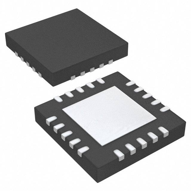
Small Footprint: 4-mm × 4-mm, Thin QFN-20
APPLICATIONS
•
•
•
•
•
•
Programmable Logic Controls (PLCs)
Industrial Process Controls (IPCs)
Telecommunications
Power-Supply Monitoring
PCB Hot-Spot Analysis
Battery-Powered Applications
In addition to having eight analog input channels, the
ADS8028 offers an internal temperature sensor with
0.25°C resolution and an internal voltage reference. A
nine-channel internal multiplexer enables multiple
channels to be selected (including the internal
temperature sensor) that are indefinitely scanned in a
sequential manner. A simple SPI-compatible serial
interface provides easy communication and control
between the device and host controller. The digital
supply can operate from 1.65 V to 5.25 V, enabling
direct interface with a wide range of processors and
controllers.
At full speed of 1 MSPS, the ADS8028 dissipates
only 17 mW. The device offers flexible power-down
modes to save power when conversions are not
being performed. The ADS8028 performance is
specified over the extended industrial temperature
range of –40°C to +125°C.
The ADS8028 is ideal for demanding measurement
applications, such as sensor output monitoring,
power-supply monitoring, and printed circuit board
(PCB) hot-spot analysis, and is available in a small
form-factor QFN-20 package.
AVDD
REF
Internal
Reference
DVDD
Buffer
AIN0
AIN1
AIN2
SH
ADC
AIN3
AIN4
AIN5
SCLK
AIN6
Control
Logic
and
Sequencer
AIN7
Internal
Temperature
Sensor
DOUT
DIN
CS
PD/RST
TM_BUSY
DGND
1
2
3
Please be aware that an important notice concerning availability, standard warranty, and use in critical applications of
Texas Instruments semiconductor products and disclaimers thereto appears at the end of this data sheet.
SPI is a trademark of Motorola.
All other trademarks are the property of their respective owners.
PRODUCTION DATA information is current as of publication date.
Products conform to specifications per the terms of the Texas
Instruments standard warranty. Production processing does not
necessarily include testing of all parameters.
Copyright © 2011–2012, Texas Instruments Incorporated
�ADS8028
SBAS549B – MAY 2011 – REVISED MARCH 2012
www.ti.com
This integrated circuit can be damaged by ESD. Texas Instruments recommends that all integrated circuits be handled with
appropriate precautions. Failure to observe proper handling and installation procedures can cause damage.
ESD damage can range from subtle performance degradation to complete device failure. Precision integrated circuits may be more
susceptible to damage because very small parametric changes could cause the device not to meet its published specifications.
ORDERING INFORMATION
PRODUCT
PACKAGE-LEAD
PACKAGE
DESIGNATOR
PACKAGE MARKING
ADS8028
QFN-20
RTJ
ADS8028IRTJ
TRANSPORT MEDIA
Tape and Reel
Tape and Reel
ABSOLUTE MAXIMUM RATINGS (1)
Over operating free-air temperature range, unless otherwise noted.
VALUE
UNIT
AVDD to DGND, AGND
–0.3 to +7
V
DVDD to DGND, AGND
–0.3 to AVDD + 0.3
V
–0.3 to +0.3
V
Analog input (AIN0 to AIN7) to AGND
–0.3 to AVDD + 0.3
V
Digital input (CS, DIN, SCLK, PD/RST) to DGND
–0.3 to DVDD + 0.3
V
Digital output (DOUT, TM_BUSY) to DGND
–0.3 to DVDD + 0.3
V
AVDD + 0.3
V
DGND to AGND
REF to AGND
Input current to any pin (except supply), continuous
±10
mA
Operating temperature range
–40 to +125
°C
Storage temperature range
–65 to +150
°C
Maximum junction temperature
Electrostatic discharge
(ESD) ratings:
(1)
2
+150
°C
Human body model (HBM)
±2000
V
Charge device model (CDM)
±500
V
Stresses above these ratings may cause permanent damage. Exposure to absolute maximum conditions for extended periods may
degrade device reliability. These are stress ratings only, and functional operation of the device at these or any other conditions beyond
those specified is not implied.
Submit Documentation Feedback
Copyright © 2011–2012, Texas Instruments Incorporated
Product Folder Link(s): ADS8028
�ADS8028
www.ti.com
SBAS549B – MAY 2011 – REVISED MARCH 2012
ELECTRICAL CHARACTERISTICS
Minimum and maximum specifications apply from TA = –40°C to +125°C. Typical specifications are at TA = +25°C.
All specifications at AVDD = 2.7 V to 5.25 V, DVDD = 1.65 V to 5.25 V, fSAMPLE = 1 MHz, fSCLK = 20 MHz, and VREF = 2.5 V
internal, unless otherwise noted.
ADS8028
PARAMETER
TEST CONDITIONS
MIN
TYP
MAX
UNIT
ANALOG INPUTS
AINx
Analog input voltage
Input capacitance
0
In sample mode
VREF
V
40
In hold mode
Input bias current
pF
8
pF
±0.01
µA
SAMPLING DYNAMICS
Conversion time
Acquisition time
Throughput rate
SCLK = 20 MHz
660
TSENSE temperature sensor channel
Full-scale step input
ns
100
µs
100
ns
SCLK = 20 MHz, AINx channel
1
MSPS
SCLK = 20 MHz, temperature
measurement channel
10
kSPS
Aperture delay
Full-power bandwidth
700
14
At 3 dB
At 0.1 dB
ns
30
MHz
10
MHz
Step response
100
ns
Overload recovery
100
ns
DC ACCURACY
Resolution
12
Bits
No missing codes
12
Bits
INL
Integral nonlinearity
±0.5
±1
LSB
DNL
Differential nonlinearity
±0.5
±0.99
LSB
±2
±4.5
LSB
±2.5
±4.5
Offset error
Offset error matching
Offset temperature drift
4
LSB
ppm/°C
Gain error
±1
±4
Gain error matching
±1
±2.5
LSB
Gain temperature drift
0.5
ppm/°C
dB
LSB
DYNAMIC PERFORMANCE
SNR
Signal-to-noise ratio
50-kHz input, –0.5 dBFS
70
72
SINAD
Signal-to-noise and distortion ratio
50-kHz input, –0.5 dBFS
70
71
THD
Total harmonic distortion
50-kHz input, –0.5 dBFS
SFDR
Spurious-free dynamic range
50-kHz input, –0.5 dBFS
–82
77.5
dB
–77
dB
84
dB
Second-order terms
–84
dB
Third-order terms
–93
dB
–100
dB
fA = 40.1 kHz, fB = 41.5 kHz
IMD
Intermodulation distortion
Channel-to-channel isolation
fIN = 50 kHz, fNOISE = 60 kHz
INTERNAL REFERENCE OUTPUT
Reference output voltage
±0.3% maximum at +25°C
Long-term stability
Output voltage hysteresis
Internal reference output impedance
(1)
2.5
2.5075
V
150
ppm
50
ppm
Ω
1
Internal reference temperature coefficient
Internal reference noise
2.4925
12
10-MHz bandwidth
60
35 (1)
ppm/°C
µVRMS
Sample tested during initial release to ensure compliance.
Submit Documentation Feedback
Copyright © 2011–2012, Texas Instruments Incorporated
Product Folder Link(s): ADS8028
3
�ADS8028
SBAS549B – MAY 2011 – REVISED MARCH 2012
www.ti.com
ELECTRICAL CHARACTERISTICS (continued)
Minimum and maximum specifications apply from TA = –40°C to +125°C. Typical specifications are at TA = +25°C.
All specifications at AVDD = 2.7 V to 5.25 V, DVDD = 1.65 V to 5.25 V, fSAMPLE = 1 MHz, fSCLK = 20 MHz, and VREF = 2.5 V
internal, unless otherwise noted.
ADS8028
PARAMETER
TEST CONDITIONS
MIN
TYP
MAX
UNIT
EXTERNAL REFERENCE INPUT
External reference input voltage range
1
DC leakage current
±0.01
AVDD
V
±1
µA
+125
°C
±3
°C
TEMPERATURE SENSOR
Operating range
–40
Accuracy
TA = –40°C to +125°C
Resolution
LSB size
±1
0.25
°C
DIGITAL INPUT AND OUTPUT
VIH
0.7 DVDD
VIL
Logic level
VOH
V
0.3 DVDD
SDO load = 20 pF, ISOURCE = 500 µA
VOL
0.8 DVDD
V
SDO load = 20 pF, ISINK = 500 µA
0.2 DVDD
Input capacitance
IIN
5
Input current
0 V < VDigitalInput < DVDD
V
V
pF
±0.01
±1
µA
POWER-SUPPLY REQUIREMENTS
AVDD
DVDD
Analog supply
Internal reference mode
2.7
3.0
5.25
External reference mode with
VEXT_REF ≤ 2.7 V
2.7
3.0
5.25
External reference mode with
VEXT_REF > 2.7 V
VEXT_REF
Digital supply
1.65
V
5.25
3.0
5.25
V
5.8
6.3
mA
7
7.5
mA
AVDD = 3.6 V, DVDD = 3.6 V
4.1
4.6
mA
AVDD = 5.25 V, DVDD = 5.25 V
4.5
5
mA
STANDBY mode
AVDD = 3.6 V, DVDD = 3.6 V
1.5
2.5
mA
Power-down mode
AVDD = 3.6 V, DVDD = 3.6 V
1
10
µA
SUPPLY CURRENT
ITOTAL
Total current (2)
Operational
Normal mode
Static
(2)
4
AVDD = 3.6 V, DVDD = 3.6 V
AVDD = 5.25 V, DVDD = 5.25 V
ITOTAL is the total current flowing in AVDD and DVDD.
Submit Documentation Feedback
Copyright © 2011–2012, Texas Instruments Incorporated
Product Folder Link(s): ADS8028
�ADS8028
www.ti.com
SBAS549B – MAY 2011 – REVISED MARCH 2012
ELECTRICAL CHARACTERISTICS (continued)
Minimum and maximum specifications apply from TA = –40°C to +125°C. Typical specifications are at TA = +25°C.
All specifications at AVDD = 2.7 V to 5.25 V, DVDD = 1.65 V to 5.25 V, fSAMPLE = 1 MHz, fSCLK = 20 MHz, and VREF = 2.5 V
internal, unless otherwise noted.
ADS8028
PARAMETER
TEST CONDITIONS
MIN
TYP
MAX
UNIT
AVDD = DVDD = 3.0 V
17
18.9
mW
AVDD = DVDD = 3.6 V
20.9
22.7
mW
AVDD = DVDD = 5.25 V
36.8
39.4
mW
AVDD = DVDD = 3.6 V
14.8
16.6
mW
AVDD = DVDD = 5.25 V
23.6
26.2
mW
STANDBY mode
AVDD = DVDD = 3.6 V
5.4
9
mW
Power-down mode
AVDD = DVDD = 3.6 V
3.6
36
µW
+125
°C
POWER CONSUMPTION
Power consumption
Operational
Normal mode
Static
TEMPERATURE
Operating temperature range
–40
THERMAL INFORMATION
ADS8028
THERMAL METRIC (1)
RTJ (QFN)
UNITS
20 PINS
θJA
Junction-to-ambient thermal resistance
32.8
θJCtop
Junction-to-case (top) thermal resistance
27.8
θJB
Junction-to-board thermal resistance
9.3
ψJT
Junction-to-top characterization parameter
0.3
ψJB
Junction-to-board characterization parameter
9.3
θJCbot
Junction-to-case (bottom) thermal resistance
1.9
(1)
°C/W
For more information about traditional and new thermal metrics, see the IC Package Thermal Metrics application report, SPRA953.
Submit Documentation Feedback
Copyright © 2011–2012, Texas Instruments Incorporated
Product Folder Link(s): ADS8028
5
�ADS8028
SBAS549B – MAY 2011 – REVISED MARCH 2012
www.ti.com
PARAMETER MEASUREMENT INFORMATION
TIMING CHARACTERISTICS
tPH_CSZ
tCONV
CS
tSU_CSCK
SCLK
1
2
t ACQ
tPH_SCLK
tSCLK
3
4
5
6
13
14
15
16
tPL_SCLK
tD_CKDO
tDV_CSDO
DOUT
3-State
ADD3
ADD2
ADD1
ADD0
tSU_CKDI
DIN
WRITE
DB11
tHT_CKDO
DB10
DB2
tDZ_CKDO
DB1
DB0
3-State
tHT_CKDI
REPEAT
AIN0
AIN1
AIN2
AIN3
EXT_REF
TMP_AVG
STANDBY
Figure 1. Serial Interface Timing Diagram
Timing Requirements for Figure 1 (1)
ADS8028
PARAMETER
DESCRIPTION
TEST CONDITIONS
MIN
TYP
MAX
UNIT
20
MHz
fSCLK
External serial clock frequency
tSCLK
External interface clock time period
tPH_SCLK
SCLK high pulse width
0.4 tSCLK
0.6 tSCLK
ns
tPL_SCLK
SCLK low pulse width
0.4 tSCLK
0.6 tSCLK
ns
tSU_CSCK + 13 tSCLK
ns
50
Conversion time:
tCONV
For channels AIN0 to AIN7
fSCLK = 20 MHz
For internal temperature sensor measurement
tPH_CSZ
CS high pulse width
tACQ
Acquisition time (for channel AINx)
tSU_CSCK
Setup time: CS to SCLK falling edge
tDV_CSDO
Delay time between CS falling edge to DOUT enabled
fSCLK = 20 MHz
ns
700
ns
100
µs
6
ns
100
ns
10
ns
17
ns
DVDD = 1.65 V to 3 V
32
ns
DVDD = 3 V to 3.6 V
29
ns
DVDD = 3.6 V to 5.25 V
28
ns
tD_CKDO
Delay time between SCLK falling edge to (new) data
available on DOUT
tHT_CKDO
Hold time: SCLK falling edge to (previous) data valid on
DOUT
10
tDZ_CKDO
Delay time between 16th SCLK falling edge to DOUT
going to high-impedance
12
tDZ_CSDO
Delay time between CS going high to DOUT going to highimpedance
tSU_CKDI
DIN setup time before SCLK falling edge
5
ns
tHT_CKDI
DIN hold time after SCLK falling edge
4
ns
tACQ_TMP
TM_BUSY falling edge to CS falling edge
tPU_STANDBY
Power-up time after coming out of STANDBY mode
tPOWER_UP
Power-up time after coming out of power-down mode
(1)
6
ns
27
ns
26
ns
100
Internal reference mode,
10-µF capacitor on REF pin
ns
1
µs
6
ms
Specifications apply from TA = –40°C to +125°C, AVDD = 2.7 V to 3.6 V, DVDD = 1.65 V to 5.25 V, VREF = 2.5 V internal, load on
DOUT = 15 pF || 100 kΩ, and tR = tF = 5 ns (10% to 90% of DVDD) and timed from a voltage level of 0.5 DVDD, unless otherwise
noted.
Submit Documentation Feedback
Copyright © 2011–2012, Texas Instruments Incorporated
Product Folder Link(s): ADS8028
�ADS8028
www.ti.com
SBAS549B – MAY 2011 – REVISED MARCH 2012
PIN CONFIGURATIONS
AIN2
AIN1
AIN0
PD/RST
DVDD
20
19
18
17
16
RTJ PACKAGE(1)
QFN-20
(TOP VIEW)
AIN3
1
15
SCLK
AIN4
2
14
DOUT
AIN5
3
13
DIN
AIN6
4
12
TM_BUSY
AIN7
5
11
CS
10
AVDD
8
NC
9
7
REF
DGND
6
AGND
Thermal Pad
(1) The exposed thermal pad on the bottom of the package must be soldered to the printed circuit board (PCB) ground for proper
functionality and heat dissipation.
NOTE: NC = no connection.
PIN ASSIGNMENTS
NAME
PIN
FUNCTION
DESCRIPTION
AGND
6
Supply
Analog ground
AIN0
18
Analog input
Analog input channel 0
AIN1
19
Analog input
Analog input channel 1
AIN2
20
Analog input
Analog input channel 2
AIN3
1
Analog input
Analog input channel 3
AIN4
2
Analog input
Analog input channel 4
AIN5
3
Analog input
Analog input channel 5
AIN6
4
Analog input
Analog input channel 6
Analog input channel 7
AIN7
5
Analog input
AVDD
10
Supply
CS
11
Digital input
DGND
9
Supply
Digital ground
DIN
13
Digital input
SPI data input
DOUT
14
Digital output
SPI data output
DVDD
16
Supply
NC
8
—
PD/RST
17
Digital input
REF
7
Analog input/output
SCLK
15
Digital input
SPI clock
Thermal pad
—
Thermal pad
Exposed thermal pad; this pin should be soldered to the PCB ground for proper
functionality and heat dissipation
TM_BUSY
12
Digital input
Busy output; this pin transitions high and remains high during conversion for
temperature sensor input
ADC operation supply voltage
Chip select; active low logic input
ADC interface supply voltage
This pin has no internal connection. Any passive component connected to this
pin does not affect device functionality.
Dual function pin for power-down and reset operation; active low logic input
ADC internal reference output or ADC external reference input
Submit Documentation Feedback
Copyright © 2011–2012, Texas Instruments Incorporated
Product Folder Link(s): ADS8028
7
�ADS8028
SBAS549B – MAY 2011 – REVISED MARCH 2012
www.ti.com
TYPICAL CHARACTERISTICS
All plots at TA = +25°C, AVDD = 3.0 V, DVDD = 3.0 V,
fSAMPLE = 1 MHz, fSCLK = 20 MHz, and VREF = 2.5 V internal, unless otherwise noted.
TYPICAL FFT
INL vs VREF
0
0.6
Amplitude (dB)
−40
Intergral Nonlinearity (LSB)
fSAMPLE = 1.176 MHz
fIN = 41.68 kHz
fSCLK = 20 MHz
SNR = 72.7 dB
THD = −93.6 dB
−20
−60
−80
−100
−120
−140
0
50
0.4
0.2
0
Minimum INL
−0.2
AVDD = 5 V
DVDD = 5 V
External Reference Mode
−0.4
−0.6
100 150 200 250 300 350 400 450 500
Input Frequency (kHz)
G000
Maximum INL
1
1.5
2
Figure 2.
2.5
3
3.5
Reference Voltage (V)
4
4.5
5
G001
Figure 3.
TYPICAL ADC INL
DNL vs VREF
0.6
1
Differential Nonlinearity (LSB)
Intergral Nonlinearity (LSB)
0.8
0.6
0.4
0.2
0
−0.2
−0.4
−0.6
0.4
Maximum DNL
0.2
0
Minimum DNL
−0.2
AVDD = 5 V
DVDD = 5 V
External Reference Mode
−0.4
−0.8
−1
0
512
1024
1536 2048 2560 3072
ADC Output Code (LSB)
3584
−0.6
4096
1
1.5
2
G002
Figure 4.
TYPICAL ADC DNL
5
G003
ENOB vs VREF
Effective Number Of Bits (ENOB)
Differential Nonlinearity (LSB)
4.5
12
0.8
0.6
0.4
0.2
0
−0.2
−0.4
−0.6
−0.8
0
512
1024
1536 2048 2560 3072
ADC Output Code (LSB)
3584
4096
11
10
9
8
AVDD = 5 V
DVDD = 5 V
External Reference Mode
1
G004
Figure 6.
8
4
Figure 5.
1
−1
2.5
3
3.5
Reference Voltage (V)
2
3
Reference Voltage (V)
4
5
G006
Figure 7.
Submit Documentation Feedback
Copyright © 2011–2012, Texas Instruments Incorporated
Product Folder Link(s): ADS8028
�ADS8028
www.ti.com
SBAS549B – MAY 2011 – REVISED MARCH 2012
TYPICAL CHARACTERISTICS (continued)
All plots at TA = +25°C, AVDD = 3.0 V, DVDD = 3.0 V,
fSAMPLE = 1 MHz, fSCLK = 20 MHz, and VREF = 2.5 V internal, unless otherwise noted.
VREF vs CURRENT LOAD
SINAD vs VREF
75
Signal to Noise and Distortion (dB)
3
Reference Voltage (V)
2.5
2
1.5
1
0.5
0
−11 −9
−7
−5
−3 −1
1
3
Current Load (mA)
5
7
9
69
66
AVDD = 5 V
DVDD = 5 V
External Reference Mode
63
60
11
1
1.5
G007
2.5
3
3.5
Reference Voltage (V)
4
4.5
5
G011
Figure 9.
SINAD vs INPUT FREQUENCY FOR VARIOUS SOURCE
IMPEDANCES
THD vs INPUT FREQUENCY FOR VARIOUS SOURCE
IMPEDANCES
Total Harmonic Distortion (dB)
−70
73
72
RIN = 200Ω
RIN = 100Ω
RIN = 50Ω
RIN = 33Ω
RIN = 0Ω
71
70
1k
10k
100k
Input Frequency (dB)
−75
−80
−85
−90
500k
RIN = 200Ω
RIN = 100Ω
RIN = 50Ω
RIN = 33Ω
RIN = 0Ω
1k
10k
100k
Input Frequency (dB)
G012
Figure 10.
PSRR vs POWER-SUPPLY RIPPLE FREQUENCY
G013
CROSSTALK vs INPUT REQUENCY
120
Channel−to−Channel Isolation
Crosstalk (dB)
−100
−120
−140
500k
Figure 11.
−80
Power −Supply Rejection
Ratio (dB)
2
Figure 8.
74
Signal to Noise and Distortion (dB)
72
1k
10k
100k
1M
10M
Supply Ripple Frequency (Hz)
100M
110
100
90
80
70
0
G014
Figure 12.
50
100 150 200 250 300 350 400 450 500
Input Frequency (dB)
G015
Figure 13.
Submit Documentation Feedback
Copyright © 2011–2012, Texas Instruments Incorporated
Product Folder Link(s): ADS8028
9
�ADS8028
SBAS549B – MAY 2011 – REVISED MARCH 2012
www.ti.com
TYPICAL CHARACTERISTICS (continued)
All plots at TA = +25°C, AVDD = 3.0 V, DVDD = 3.0 V,
fSAMPLE = 1 MHz, fSCLK = 20 MHz, and VREF = 2.5 V internal, unless otherwise noted.
AVDD POWER vs THROUGHPUT
(AVDD = 3 V)
AVDD POWER vs THROUGHPUT
(AVDD = 5 V)
20
30
17
AVDD Power − Normal
Operation Mode (mW)
AVDD Power − Normal
Operation Mode (mW)
AVDD = 3 V
DVDD = 3 V
14
11
8
26
22
18
14
AVDD = 5 V
DVDD = 5 V
5
0
200
400
600
Throughput (kSPS)
800
10
1000
200
1000
G017
POWER-DOWN CURRENT vs AVDD AT VARIOUS
TEMPERATURES
AVDD CURRENT vs THROUGHPUT
(AVDD = 3 V)
6
3
AVDD Supply Current − Normal
Operation Mode (mA)
125°C
85°C
25°C
−40°C
2
1
3.2
3.7
4.2
4.7
AVDD, Analog Supply Voltage (V)
5
4
3
2
0
5.2
AVDD = 3 V
DVDD = 3 V
1
0
200
G018
Figure 16.
400
600
Throughput (kSPS)
800
1000
G019
Figure 17.
AVDD CURRENT vs THROUGHPUT
(AVDD = 5 V)
DNL vs TEMPERATURE
6
1
0.8
Differential Nonlinearity (LSB)
AVDD Supply Current − Normal
Operation Mode (mA)
800
Figure 15.
0
2.7
5
4
3
2
1
0
AVDD = 5 V
DVDD = 5 V
0
200
400
600
Throughput (kSPS)
800
0.6
Maximum DNL
0.4
0.2
0
Minimum DNL
−0.2
−0.4
−0.6
−0.8
1000
−1
−40
G020
Figure 18.
10
400
600
Throughput (kSPS)
Figure 14.
4
AVDD Supply Current − Power
Down Mode (uA)
0
G016
−15
10
35
60
85
Free−Air Temperature (°C)
110 125
G021
Figure 19.
Submit Documentation Feedback
Copyright © 2011–2012, Texas Instruments Incorporated
Product Folder Link(s): ADS8028
�ADS8028
www.ti.com
SBAS549B – MAY 2011 – REVISED MARCH 2012
TYPICAL CHARACTERISTICS (continued)
All plots at TA = +25°C, AVDD = 3.0 V, DVDD = 3.0 V,
fSAMPLE = 1 MHz, fSCLK = 20 MHz, and VREF = 2.5 V internal, unless otherwise noted.
INL vs TEMPERATURE
OFFSET ERROR vs TEMPERATURE
1
4
0.6
Maximum INL
0.4
Offset Error (LSB)
Integral Nonlinearity (LSB)
0.8
0.2
0
Minimum INL
−0.2
−0.4
2
0
−2
−0.6
−0.8
−1
−40
−15
10
35
60
85
Free− Air Temperature (dB)
−4
−40
110 125
−15
G022
Figure 20.
GAIN ERROR vs TEMPERATURE
SINAD vs AVDD
Signal to Noise and Distortion (dB)
Gain Error (LSB)
0
−2
−15
10
35
60
85
Free−Air Temperature (°C)
72
69
66
63
DVDD = 1.8 V
60
2.7
110 125
3.2
3.7
4.2
4.7
AVDD, Analog Supply Voltage (V)
G025
Figure 22.
5.2
G026
Figure 23.
DNL vs AVDD
INL vs AVDD
1
1
0.8
0.6
Integral Nonlinearity (LSB)
0.8
Differential Nonlinearity (LSB)
G024
75
2
Maximum DNL
0.4
0.2
0
−0.2
Minimum DNL
−0.4
−0.6
−0.8
−1
2.7
110 125
Figure 21.
4
−4
−40
10
35
60
85
Free−Air Temperature (°C)
0.6
0.2
0
3.7
4.2
4.7
5.2
AVDD, Analog Supply Voltage (V)
5.7
Minimum INL
−0.2
−0.4
−0.6
−0.8
3.2
Maximum INL
0.4
DVDD = 1.8 V
−1
2.7
G027
Figure 24.
3.2
3.7
4.2
4.7
AVDD, Analog Supply Voltage (V)
5.2
G028
Figure 25.
Submit Documentation Feedback
Copyright © 2011–2012, Texas Instruments Incorporated
Product Folder Link(s): ADS8028
11
�ADS8028
SBAS549B – MAY 2011 – REVISED MARCH 2012
www.ti.com
TYPICAL CHARACTERISTICS (continued)
All plots at TA = +25°C, AVDD = 3.0 V, DVDD = 3.0 V,
fSAMPLE = 1 MHz, fSCLK = 20 MHz, and VREF = 2.5 V internal, unless otherwise noted.
GAIN ERROR vs AVDD
4
2
2
Gain Error (LSB)
Offset Error (LSB)
OFFSET ERROR vs AVDD
4
0
−2
0
−2
DVDD = 1.8 V
−4
2.7
DVDD = 1.8 V
3.2
3.7
4.2
4.7
AVDD, Analog Supply Voltage (V)
−4
2.7
5.2
3.2
3.7
4.2
4.7
AVDD, Analog Supply Voltage (V)
G030
Figure 26.
CROSSTALK vs INPUT FREQUENCY
TEMPERATURE SENSOR ACCURACY
1.5
105
1
100
Error in Temperature
Measurement (°C)
Memory Cross Talk (dB)
G031
Figure 27.
110
95
90
85
80
0.5
0
−0.5
−1
75
70
5.2
0
100
200
300
Input Frequency (kHz)
400
−1.5
−40 −25 −10
500
5
20 35 50 65
Temperature (°C)
G032
Figure 28.
80
95
110 125
G034
Figure 29.
TEMPERATURE SENSOR RESPONSE TO THERMAL SHOCK
– FROM ROOM TEMPERATURE INTO 50°C STIRRED OIL
Temperature Reading (°C)
60
50
40
30
20
10
0
0
20
40
60
Time (Seconds)
80
100
G034
Figure 30.
12
Submit Documentation Feedback
Copyright © 2011–2012, Texas Instruments Incorporated
Product Folder Link(s): ADS8028
�ADS8028
www.ti.com
SBAS549B – MAY 2011 – REVISED MARCH 2012
OVERVIEW
The ADS8028 is a 12-bit successive-approximation register (SAR) analog-to-digital converter (ADC) that can
support throughput rates up to 1 MSPS. The device features a 2.5-V internal reference, but can also function
with an external reference source. The analog input range is 0 V to VREF. The device supports eight single-ended
analog inputs and integrates an internal temperature sensor. A nine-channel (eight analog inputs plus the internal
temperature sensor) internal multiplexer allows selection of multiple channels to be scanned sequentially.
Additionally, this scan sequence can be repeated indefinitely with minimal intervention.
The internal temperature sensor has a resolution of 0.25°C and measures the ADS8028 die temperature. To
measure the temperature of an external heat source, thermal resistance should be minimized between the heat
source and the ADS8028 thermal pad (refer to the Application Information section for more details).
The ADS8028 consumes only 17 mW of power at 1 MSPS and also provides hardware (PD) and software
(STANDBY) selectable low-power modes for optimal power usage.
The device provides an SPI-compatible serial interface that can operate up to 20 MHz over a wide supply range
(DVDD = 1.65 V to 5.25 V). The ADS8028 operates with one cycle latency, thus the conversion result performed
in one cycle can be read out in the subsequent cycle.
ANALOG INPUTS AND MULTIPLEXER
The ADS8028 has eight single-ended analog input channels (AIN0 to AIN7). Figure 31 shows an equivalent
circuit for each analog input pin. The two diodes, D1 and D2, provide electrostatic discharge (ESD) protection for
the individual analog pins. These diodes can conduct approximately 10 mA of current without causing irreversible
damage to the device. Diode D1 turns on when AINx is greater than AVDD + 0.3 V and diode D2 turns on when
AINx is less than AGND – 0.3 V. Therefore, care must be taken to always ensure that Equation 1 is met.
AGND – 0.3 V < AINx < AVDD + 0.3 V
(1)
AVDD
D1
SW
RS
CSAMPLE
AINx
CPIN
D2
SW is closed during sampling.
SW is open during conversion.
Figure 31. Equivalent Analog Input Circuit
Capacitor CPIN is approximately 8 pF. Resistor RS represents the sampling switch on-state resistance plus the
input multiplexer on-state resistance. The total resistance is approximately 130 Ω. CSAMPLE is the ADC sampling
capacitor, typically 40 pF.
The ADS8028 contains a nine-channel input multiplexer that either allows one of the eight analog input channels
or the internal temperature sensor to be converted. Multiple channels can be converted in a predetermined
sequence; this sequence can be repeated indefinitely with appropriate Control Register settings (refer to the
Modes of Operation section for more details). On power-up, no channel is selected for conversion and SDO
returns all '1's. One write cycle must be executed to select the channels and start the conversion process.
In order to achieve specified signal-to-noise ratio (SNR) and total-harmonic-distortion (THD) performance,
especially at higher input frequencies, it is recommended to drive each analog input pin with a low impedance
source. An external amplifier can also be used to drive the input pins. A simple RC low-pass filter can be used on
the analog input pins to reduce the input signal bandwidth and remove the noise components at higher
frequencies (refer to the Application Information section for more details).
Submit Documentation Feedback
Copyright © 2011–2012, Texas Instruments Incorporated
Product Folder Link(s): ADS8028
13
�ADS8028
SBAS549B – MAY 2011 – REVISED MARCH 2012
www.ti.com
TEMPERATURE SENSOR
The internal temperature sensor measures the ADS8028 die temperature. The temperature sensor can be
selected for conversion by setting the TSENSE bit in the Control Register to '1'. The TM_BUSY pin goes high as
soon as the temperature sensor is selected for conversion and remains high until the conversion is completed
(100 µs, max).
The operating temperature range for this internal temperature sensor is limited by the operating temperature
range of the ADS8028 (–40°C to +125°C).
Modes of Operation
The ADS8028 temperature sensor can operate in two modes: normal mode and averaging mode.
Normal Mode
To operate in normal mode (without the averaging feature), the TMP_AVG bit in the Control Register should be
set to '0' and the TSENSE bit in the Control Register should be set to '1'. Output data are the result of a single
conversion performed on the temperature sensor. This mode is the default mode of operation for the temperature
sensor. A single conversion on the temperature sensor takes 100 µs, max.
Averaging Mode
In this mode, the ADS8028 provides rolling average filtering to increase the accuracy of the temperature sensor
measurement. To activate this filter, the TMP_AVG bit in the Control Register should be set to '1'. This bit must
be set to '1' in subsequent write operations for the duration of the filter operation. Resetting the TMP_AVG bit to
'0' resets and deactivates the filter and places the ADS8028 in a normal mode of operation.
When the TMP_AVG and TSENSE bits are both set to '1', the temperature sensor is selected and the conversion
result is sent to the filter block. The filter block output is given by Equation 2:
New_Average_Result = 7 (Previous_Average_Result) + 1 (Current_Result)
8
8
(2)
This output can be read during the next conversion cycle. After enabling the averaging feature, the first ADS8028
output data are the same as the temperature sensor conversion result. Averaging starts taking effect from the
subsequent conversion performed on the temperature sensor.
Temperature Sensor Data Format
The temperature sensor, along with the ADC, gives 0.25°C resolution over the operating temperature range. The
temperature reading from the ADC is in 12-bit twos complement format, as shown in Table 1.
Table 1. Temperature Data Format
14
TEMPERATURE (°C)
DIGITAL OUTPUT
–40
1111 0110 0000
–25
1111 1001 1100
–10
1111 1101 1000
–0.25
1111 1111 1111
0
0000 0000 0000
+0.25
0000 0000 0001
+10
0000 0010 1000
+25
0000 0110 0100
+50
0000 1100 1000
+75
0001 0010 1100
+100
0001 1001 0000
+105
0001 1010 0100
+125
0001 1111 0100
Submit Documentation Feedback
Copyright © 2011–2012, Texas Instruments Incorporated
Product Folder Link(s): ADS8028
�ADS8028
www.ti.com
SBAS549B – MAY 2011 – REVISED MARCH 2012
If the output data MSB is ‘0’, the temperature can be calculated with Equation 3:
Temperature = VEXT_REF
ADC_Code
10
+ 109.3 - 273.15
where:
VEXT_REF is the value of the external reference voltage
(3)
If the output data MSB is ‘1’, the temperature can be calculated with Equation 4:
Temperature = VEXT_REF
ADC_Code - 4096
+ 109.3 - 273.15
10
where:
VEXT_REF is the value of the external reference voltage
(4)
For a 2.5-V reference (internal or external), Equation 3 and Equation 4 simplify to Equation 5 and Equation 6,
respectively.
ADC_Code
Positive Temperature =
(5)
4
Negative Temperature =
4096 - ADC_Code
4
(6)
REFERENCE
The ADS8028 can operate with either an internal voltage reference or an optional external reference. The type of
reference used is set by the EXT_REF bit in the Control Register.
The internal reference is selected when the EXT_REF bit is set to '0'. A 2.5-V output of the internal reference is
available on the REF pin. A 10-µF decoupling capacitor is recommended between the REF and AGND pins. The
reference circuit requires 5.5 ms to charge the decoupling capacitor. The internal reference is capable of
sourcing up to 2 mA of current and is designed to drive the ADS8028. It is recommended to buffer this output for
use elsewhere in the system.
The ADS8028 can operate with an external reference when the EXT_REF bit is set to '1'. An external reference
can be supplied through the REF pin. By default, the ADS8028 powers up in internal reference mode and must
be programmed to function with an external reference. Until such a time, the ADS8028 draws additional current
from the external reference source. This current is limited to 20 mA, using internal protection circuitry. Texas
Instruments' REF5025 can be used as external reference source for the ADS8028.
Submit Documentation Feedback
Copyright © 2011–2012, Texas Instruments Incorporated
Product Folder Link(s): ADS8028
15
�ADS8028
SBAS549B – MAY 2011 – REVISED MARCH 2012
www.ti.com
ADC TRANSFER FUNCTION
The ADS8028 output is in straight binary format for all analog input channels (AIN0 to AIN7) and is in twos
complement format for the temperature sensor conversion result. The transition in output code occurs at every
LSB step. For the ADS8028, LSB step size is VREF/4096. The ideal ADS8028 transfer characteristic for straight
binary coding is shown in Figure 32.
ADC Code (Hex)
3FFF
2000
0001
1 LSB
FSR/2
FSR - 1 LSB
VIN
Single-Ended Analog Input
Figure 32. Straight Binary Transfer Characteristic
16
Submit Documentation Feedback
Copyright © 2011–2012, Texas Instruments Incorporated
Product Folder Link(s): ADS8028
�ADS8028
www.ti.com
SBAS549B – MAY 2011 – REVISED MARCH 2012
SERIAL INTERFACE
Figure 33 shows a detailed ADS8028 serial interface timing diagram. The device uses the serial clock (SCLK) for
internal conversion and for data transfer into and out of the device.
The CS signal defines one frame of conversion and serial transfer. The ADS8028 samples the analog input on
the CS falling edge. The sample-and-hold circuit enters into hold mode and the serial data bus comes out of 3state. The subsequent 16 SCLK cycles are used for conversion and data transfer. As shown in Figure 33, the
MUX selects the programmed channel and the sample-and-hold circuit enters into hold mode on the 14th SCLK
falling edge. The DOUT pin goes back to 3-state on the 16th SCLK falling edge or on the CS rising edge
(whichever occurs first). For a valid read or write operation to the ADS8028, 16 clocks must be provided on the
SCLK pin between the CS falling edge to the subsequent CS rising edge. If the CS rising edge occurs before 16
SCLKs have elapsed, the conversion is terminated, the DOUT line goes back into 3-state, and the Control
Register is not updated.
Start of Sampling
CS
SCLK
DOUT
DIN
1
3-State
ADD3
WRITE
2
ADD2
REPEAT
3
ADD1
4
ADD0
CH0
CH1
5
DB11
CH2
6
DB10
CH3
13
14
DB2
EXT_REF
15
DB1
TMP_AVG
16
DB0
3-State
STANDBY
Figure 33. Serial Interface Timing Diagram
Refer to Table 3 for the ADS8028 output data format. Bits ADD[3:0] specify the channel selected for conversion
and bits DB[11:0] are the conversion result for the selected channel.
A CS falling edge brings the DOUT pin out of 3-state and also outputs the ADD3 bit on the DOUT pin. The next
15 bits of data (ADD2 to DB0) are clocked out on the subsequent SCLK falling edges. Therefore, the first SCLK
falling edge outputs the ADD2 bit on DOUT and can also be used by the microcontroller or digital signal
processor (DSP) to read the first bit (ADD3). Similarly, bit DB0 is clocked out on the 15th SCLK falling edge and
can be read by the microcontroller or DSP on the 16th SCLK falling edge. The 16th SCLK falling edge also puts
the DOUT pin into 3-state.
When using a slower SCLK, it may be possible for the microcontroller or DSP to read the data on each SCLK
rising edge. The first SCLK rising edge (after the CS falling edge) reads ADD3 and the 15th SCLK rising edge
reads DB0.
Data provided on the DIN pin are clocked into the ADS8028 on the first 16 SCLK falling edges (after the CS
falling edge). However, if the WRITE bit is not set to '1', the ADS8028 ignores the subsequent 15 bits of data
(refer to the Data Write Operation section for more details).
Submit Documentation Feedback
Copyright © 2011–2012, Texas Instruments Incorporated
Product Folder Link(s): ADS8028
17
�ADS8028
SBAS549B – MAY 2011 – REVISED MARCH 2012
www.ti.com
DATA WRITE OPERATION
Control Register Settings
The ADS8028 operation is controlled by the status of the internal Control Register. Data written into the Control
Register decide the configuration of the ADS8028 for the next conversion cycle. The Control Register is 16 bits
wide, and only supports write operation. The Control Register can be written to with the serial interface. Data on
the DIN pin are loaded into the Control Register on the first 16 SCLK falling edges (after a CS falling edge). The
bit functions are outlined in Table 2. On power-up, the default Control Register content is all '0's.
Table 2. Control Register Bit Functions
MSB
15
14
13
12
11
10
9
8
WRITE
REPEAT
AIN0
AIN1
AIN2
AIN3
AIN4
AIN5
7
6
5
4
3
2
1
0
AIN6
AIN7
TSENSE
X
X
EXT_REF
TMP_AVG
STANDBY
LSB
Bit 15
WRITE: Write to Control Register
Enable write operation.
0 = Write disabled; Control Register is not updated and the next 15 bits are ignored (default)
1 = Write enabled; the next 15 bits update the Control Register
Bit 14
REPEAT: Repeat conversion mode
Enable conversion repeat mode (refer to the Modes of Operation section).
0 = Disable repeat conversion mode (default)
1 = Enable repeat conversion mode
Bits[13:6]
AIN[0:7]: Analog input channel selection
Each AINx bit corresponds to the associated analog input channel, AIN0 to AIN7.
0 = AINx channel is not selected for conversion (default)
1 = AINx channel is selected for conversion
Bit 5
TSENSE: Internal temperature sensor selection
Internal temperature sensor selection for conversion in subsequent cycles.
0 = Internal temperature sensor output is not selected for conversion (default)
1 = Internal temperature sensor output is selected for conversion
Bits[4:3]
X: Don’t care
Bit 2
EXT_REF: Reference source selection
This bit selects the reference source for the next conversion.
0 = Internal reference is used for the next conversion (default)
1 = External reference is used for the next conversion
Bit 1
TMP_AVG: Temperature sensor averaging selection
This bit selects the mode of operation for the temperature sensor channel; this bit is ignored
if bit 5 is set to '0'.
0 = Averaging is disabled on the temperature sensor result (default)
1 = Averaging is enabled on the temperature sensor result
Bit 0
STANDBY: STANDBY mode selection
This bit sets the mode (normal or standby) for the ADS8028.
0 = The ADS8028 operates in normal mode (default)
1 = The ADS8028 goes to standby mode in the next cycle
18
Submit Documentation Feedback
Copyright © 2011–2012, Texas Instruments Incorporated
Product Folder Link(s): ADS8028
�ADS8028
www.ti.com
SBAS549B – MAY 2011 – REVISED MARCH 2012
DATA READ OPERATION
Table 3 shows the ADS8028 output data format. Bits ADD[3:0] specify the channel selected for conversion and
bits DB[11:0] are the conversion result for the selected channel.
Table 3. Channel Address Bits
ADD3
ADD2
ADD1
ADD0
ANALOG INPUT CHANNEL
0
0
0
0
AIN0
0
0
0
1
AIN1
0
0
1
0
AIN2
0
0
1
1
AIN3
0
1
0
0
AIN4
0
1
0
1
AIN5
0
1
1
0
AIN6
0
1
1
1
AIN7
1
0
0
0
TSENSE without averaging
1
0
0
1
TSENSE with averaging
Analog Input Channel
A CS falling edge brings the DOUT pin out of 3-state and also outputs the ADD3 bit on the DOUT pin. The next
15 bits of data (ADD2 to DB0) are clocked out on the subsequent SCLK falling edges. Therefore, the first SCLK
falling edge outputs the ADD2 bit on DOUT and can also be used by the microcontroller or DSP to read the first
bit (ADD3). Similarly, bit DB0 is clocked out on the 15th SCLK falling edge and can be read by the
microcontroller or DSP on the 16th SCLK falling edge. The 16th SCLK falling edge also puts the DOUT pin into
3-state.
When using a slower SCLK, it may be possible for the microcontroller or DSP to read the data on each SCLK
rising edge. The first SCLK rising edge (after the CS falling edge) reads ADD3 and the 15th SCLK rising edge
reads DB0.
Submit Documentation Feedback
Copyright © 2011–2012, Texas Instruments Incorporated
Product Folder Link(s): ADS8028
19
�ADS8028
SBAS549B – MAY 2011 – REVISED MARCH 2012
www.ti.com
Internal Temperature Sensor Channel
The internal temperature sensor can be selected for conversion by writing a '1' to the TSENSE bit in the Control
Register. On the next CS falling edge, the TM_BUSY pin goes high and remains high throughout the temperature
sensor conversion process. When the TM_BUSY pin goes high, 16 clocks are required to execute one valid read
or write cycle: to read the previous conversion result and to program the next conversion settings. However, any
subsequent read or write operations are ignored until TM_BUSY goes low; CS is ignored, the Control Register is
not updated, and DOUT returns all '1's.
The ADS8028 takes 100 μs (max) to measure and convert the temperature channel. A TM_BUSY signal falling
edge can be used to initiate a read operation in order to read the temperature conversion result. However, tACQ
must be allowed to elapse between the TM_BUSY falling edge and the subsequent CS falling edge to ensure
that the subsequent conversion has sufficient acquisition time. Figure 34 shows the temperature sensor
conversion sequence.
After TM_BUSY goes high, the temperature conversion can be aborted by writing a '1' to the STANDBY bit in the
first write operation. The device aborts the ongoing conversion and enters STANDBY mode on the 16th SCLK
falling edge.
Integrating and Converting
for TSENSE
Waiting for Configuration
tACQ
Converting for Channel AIN0
CS
1
1
16
1
16
16
SCLK
DOUT
DIN
Invalid Data
Invalid Data
Conversion Result for
Temperature Measurement
Command:
Select Channel TSENSE
Command:
Select Channel AIN0
No Write to the
Control Register
TM_BUSY
Figure 34. Serial Interface Timing Diagram for the Temperature Sensor Conversion
MODES OF OPERATION
Channel Scanning
The ADS8028 offers different modes of operation that can be selected by programming the Control Register.
Channel-scanning modes enable any of the nine channels to be selected for conversion and also allow the
selected channels to be repeatedly converted. Low-power modes allow power consumption and throughput rate
ratio to be optimized.
Single or Multiple Channels: One Conversion
The ADS8028 can be configured to convert any of the nine channels by writing a '1' to the Control Register bit
associated with the desired channel. After power-up, a valid write operation must be executed on the Control
Register to select the desired channel. In this mode, the REPEAT bit in the Control Register should be set to '0'.
The selected channel is converted in the second frame and the conversion result can be clocked out in the third
frame. During the second frame, the Control Register can be written to select the channel to be converted in the
third frame. Figure 35 shows a diagram of this configuration.
Waiting for Configuration
Converting for Channel AIN3
Converting for Channel AIN5
Converting for Channel AIN1
CS
1
16
1
16
1
16
1
16
SCLK
DOUT
DIN
Invalid Data
Invalid Data
Conversion Result for
Channel AIN3
Conversion Result for
Channel AIN5
Command:
Select Channel AIN3
Command:
Select Channel AIN5
Command:
Select Channel AIN1
Command:
Select Channel AINx
Figure 35. Configuring a Conversion and Read with the ADS8028
(One Channel Selected for Conversion, REPEAT = 0)
20
Submit Documentation Feedback
Copyright © 2011–2012, Texas Instruments Incorporated
Product Folder Link(s): ADS8028
�ADS8028
www.ti.com
SBAS549B – MAY 2011 – REVISED MARCH 2012
If multiple channels are selected by writing a '1' to all associated bits in the Control Register, the ADS8028
converts all selected channels sequentially (in ascending order) in successive frames as defined by the CS
falling edges. When all selected channels in the Control Register are converted, the ADS8028 stops conversions
and waits for a valid write operation to be executed in the Control Register to select the next channel to be
converted. This operation is shown in Figure 36. DOUT returns all '1's if the conversion sequence is completed
or if no channel is selected. When the ADS8028 begins to convert the first channel in the selected channel
sequence, the WRITE bit in the Control Register must be set to '0' in any subsequent frames to avoid interrupting
the selected sequence.
Waiting for Configuration
Converting for Channel AIN2
Converting for Channel AIN7
CS
¼
1
16
1
16
1
16
¼
SCLK
Invalid Data
Invalid Data
Conversion Result for Channel AIN2
¼
Command: Select Channels
AIN2 and AIN7
No Write to the Control Register
Command: Select Channel AIN0
¼
Converting for Channel AIN0
Waiting for Configuration
DOUT
DIN
CS
1
16
16
1
SCLK
DOUT
DIN
Conversion Result for Channel AIN7
Conversion Result for Channel AIN0
No Write to the Control Register
No Write to the Control Register
Figure 36. Configuring a Conversion and Read with the ADS8028
(Numerous Channels Selected for Conversion, REPEAT = 0)
Single or Multiple Channels: Repeated Conversions
The ADS8028 can be programmed to repeatedly convert either a single channel or a sequence of channels
without having to reprogram the Control Register. To operate in this mode, execute a valid write operation to the
Control Register. During this write operation, the REPEAT bit in the Control Register should be set to '1' and the
desired channels should be selected by writing a '1' to the associated bits. Thereafter, the ADS8028 continuously
cycles through the selected channels in ascending order, beginning with the lowest channel and converting all
channels selected in the Control Register. On completion of the sequence, the ADS8028 returns to the first
selected channel in the Control Register and repeats the sequence.
Submit Documentation Feedback
Copyright © 2011–2012, Texas Instruments Incorporated
Product Folder Link(s): ADS8028
21
�ADS8028
SBAS549B – MAY 2011 – REVISED MARCH 2012
www.ti.com
The ADS8028 continues to operate in repeat mode until a valid write operation is executed to reprogram the
Control Register. When the Control Register is updated, the ADS8028 comes out of repeat mode and begins
operating as per the new programmed settings. Therefore, to continue in repeat mode and to avoid accidentally
overwriting the Control Register, it is recommended that the WRITE bit in the Control Register be set to '0' while
operating in repeat mode. Figure 37 illustrates the repeat mode of operation.
Waiting for Configuration
Converting for Channel AIN2
Converting for Channel AIN5
1
1
¼
CS
1
16
16
16
¼
SCLK
Invalid Data
Invalid Data
Conversion Result for
Channel AIN2
¼
Command: Select Channels
AIN2, AIN5, and AIN7, Repeat = 1
No Write to the Control Register
No Write to the Control Register
¼
Converting for Channel AIN7
Converting for Channel AIN2
Converting for Channel AIN5
1
1
DOUT
DIN
CS
1
16
16
16
SCLK
DOUT
DIN
Conversion Result for
Channel AIN5
Conversion Result for
Channel AIN7
Conversion Result for
Channel AIN2
No Write to the Control Register
No Write to the Control Register
No Write to the Control Register
Figure 37. Configuring a Conversion and Read in Repeat Mode
Low-Power Modes
In normal mode of operation, all internal ADS8028 blocks are always powered up and the device is always ready
to initiate a new conversion. This architecture enables the ADS8028 to support the 1-MSPS rated throughput
rate. However, the ADS8028 also supports two low-power modes that can be used to optimize the power
consumption and throughput rate ratio. In these low-power modes, some internal ADS8028 blocks are powered
up or down as the operation requires. This flexibility reduces the overall power consumption at lower throughput
rates.
STANDBY Mode
In STANDBY mode, only part of the ADS8028 internal circuitry is powered down. The internal reference is not
powered down and, therefore, the ADS8028 can be fully powered up within 1 µs. To enter STANDBY mode, a
valid write operation should be executed to the Control Register with the STANDBY bit set to '1'. The ADS8028
enters STANDBY mode on the CS rising edge following this write operation.
The temperature sensor averaging function is also reset when the device enters STANDBY mode. While in
STANDBY mode, any read operation on the ADS8028 returns all '1's on the DOUT pin.
The ADS8028 remains in STANDBY mode until the STANDBY bit in the Control Register is reset to '0' using a
valid write operation. Then, the ADS8028 starts powering up on the CS rising edge following this write operation.
One valid Control Register write cycle must complete in order to update the desired channels for subsequent
conversions. After successful completion of these two write cycles, the device enters a normal mode of operation
and operates with one cycle latency.
22
Submit Documentation Feedback
Copyright © 2011–2012, Texas Instruments Incorporated
Product Folder Link(s): ADS8028
�ADS8028
www.ti.com
SBAS549B – MAY 2011 – REVISED MARCH 2012
It takes four serial transfer cycles for the ADS8028 to exit STANDBY mode and transmit the first valid conversion
data, as shown in Figure 38. The first cycle updates the STANDBY bit to '0'; the second cycle selects the
channels and operation mode; the third cycle converts the selected channel; and the result of this conversion can
be clocked out in the fourth cycle.
Device Starts to Exit
Standby Mode
Device Enters
Standby Mode
Waiting for Configuration
In Standby Mode
In Standby Mode
¼
CS
1
16
1
16
1
16
¼
SCLK
Invalid Data
1111 1111 1111
1111 1111 1111
¼
Command: Enter Standby Mode,
STANDBY = 1
No Write to the
Control Register
Command: Exit Standby Mode,
STANDBY = 0
¼
DOUT
DIN
Waiting for Configuration
Device Exits
Standby Mode
Converting for Channel AIN1
Converting for Channel AIN 4
CS
1
16
1
16
1
16
SCLK
Invalid Data
Invalid Data
Conversion Result for
Channel AIN1
Command: Select Channel AIN1,
STANDBY = 0
Command:
Select Channel AIN4
No Write to the
Control Register
DOUT
DIN
Figure 38. STANDBY Mode of Operation
Power-Down Mode
In power-down mode, all internal ADS8028 circuitry (including the internal reference) is powered down and the
Control Register is reset to the default values. The temperature sensor averaging feature is reset and disabled.
The ADS8028 can be placed into power-down mode by pulling the PD/RST pin to a logic low state for at least 90
ns. The PD/RST pin is asynchronous to the clock; thus, it can be triggered at any time regardless of the status of
other ADS8028 pins (including the analog input channels). When the device is in power-down mode, any activity
on the digital input pins (apart from the PD/RST pin) is ignored and the device does not take input-dependent
current from the analog input pins.
The ADS8028 powers up in default condition when the PD/RST pin is pulled back to a logic high level.
Conversions can begin when tPOWER_UP has elapsed.
Submit Documentation Feedback
Copyright © 2011–2012, Texas Instruments Incorporated
Product Folder Link(s): ADS8028
23
�ADS8028
SBAS549B – MAY 2011 – REVISED MARCH 2012
www.ti.com
RESET
The ADS8028 can be RESET by pulling the PD/RST pin to a logic low state for no longer than 60 ns. This input
is asynchronous to the clock. On RESET, the Control Register bits are set to the default state and the
temperature sensor averaging feature is reset and disabled. When the PD/RST is pulled back to a logic high
state, the ADS8028 is placed in normal mode. One valid write operation must be executed on the Control
Register in order to configure the ADS8028 and to select the channels before initiating conversions.
Note that PD/RST is a dual-function pin. Figure 39 shows the timing of this pin and Table 4 explains the usage of
this pin.
tPL_PDRST
PD/RST
Figure 39. PD/RST Pin Timing
Table 4. PD/RST Pin Functionality
CONDITION
tPL_PDRST < 60 ns
60 ns < tPL_PDRST < 90 ns
tPL_PORST > 90 ns
DEVICE MODE
RESET (device does not enter power-down mode)
Device RESET. The ADS8028 may or may not enter power-down
mode.
This setting is not recommended.
Device enters power-down mode
POWER SUPPLY
The ADS8028 has two separate power supplies: AVDD and DVDD. The ADC operates on an AVDD power
supply; the DVDD supply is used for the interface circuits. AVDD and DVDD can be set independently to any
value within the permissible range; however, care must be taken to ensure that Equation 7 is fulfilled.
DVDD ≤ AVDD + 0.3 V
(7)
The ADS8028 contains an internal power-on-reset (POR) circuit that resets the Control Register to the default
value (all zeros). Therefore, by default, the ADS8028 powers up in internal reference mode. To continue with the
internal reference, a 5.5-ms delay must elapse before initiating the first conversion.
To operate with an external reference, there is no required delay for the internal reference to power-up. The
ADS8028 digital interface is fully functional 500 µs after power-up. Therefore, after a 500-µs delay, a valid write
operation can be executed to the Control Register to program the device in external reference mode and to
select the channels for conversion.
24
Submit Documentation Feedback
Copyright © 2011–2012, Texas Instruments Incorporated
Product Folder Link(s): ADS8028
�ADS8028
www.ti.com
SBAS549B – MAY 2011 – REVISED MARCH 2012
APPLICATION INFORMATION
USAGE OF INTERNAL TEMPERATURE SENSOR
The ADS8028 accurately measures and converts the temperature of its own silicon die. Most of the heat transfer
between any external heat source and the ADS8028 die occurs via the thermal pad. Therefore, the ADS8028
can be used to measure the temperature of any external heat source by minimizing the thermal resistance
between the heat source and the device thermal pad.
APPLICATION CIRCUITS
ADC Driver
The OPA836 is a low-power, 205-MHz bandwidth op amp with 560-V/μs slew rate, and is an excellent driver for
the ADS8028 SAR ADC for high ac performance at maximum throughput (1 MSPS). The high bandwidth of the
OPA836 is able to correct for fast load transients created by the SAR ADC switching behavior. An RC circuit
inserted between the OPA836 and ADS8028 is recommended to further aid the overall circuit performance. This
configuration is shown in Figure 40. The RC filter effectively limits the full-power bandwidth of the ADS8028 to
reduce the overall noise bandwidth and peak-to-peak noise sampled by the ADS8028. The capacitance is sized
to be 10 to 20 times larger than the internal ADS8028 sampling capacitor to provide quick charge sharing to the
ADC during switching transients. Furthermore, the resistor provides some isolation between the OPA836 output
and the capacitive load to stabilize the amplifier. The RC circuit –3-dB cutoff frequency should be an order of
magnitude or larger than the highest input signal frequency to avoid attenuating the desired input signal. A
collection of other ADC driving circuits can be found in application note Buffer Op Amp to ADC Circuit Collection
(SLOA098).
VS+
VS+
+
24.9Ÿ
ADS8028
OPA836
0V W 2.5V ADC
Input Range
AC
430 pF
Figure 40. OPA836 Buffer
The TINA-TI simulation file of this circuit can be downloaded by clicking the following link: OPA836 Buffer.
Submit Documentation Feedback
Copyright © 2011–2012, Texas Instruments Incorporated
Product Folder Link(s): ADS8028
25
�ADS8028
SBAS549B – MAY 2011 – REVISED MARCH 2012
www.ti.com
The ac performance of the circuit in Figure 40 was tested with a 2.36-VPP (–0.5 dBFS), 49.911499023-kHz input
sine wave. The FFT of the sampled input signal with 8192 samples is shown in Figure 41. The high-precision
input signal frequency used to achieve coherent sampling without a windowing function is applied to the data
prior to the Fourier Transform. Figure 41 shows that this driver circuit allows the ADS8028 to operate at full
throughput within typical characteristic specifications.
0
AVDD = 5 V
VREF = 2.5 V internal
fSAMPLE = 1 MHz
fIN = 49.9115 kHz
fSCLK = 20 MHz
SNR =72.145 dB
THD = −87.844 dB
−20
Amplitude (dB)
−40
−60
−80
−100
−120
−140
0
50
100 150 200 250 300 350 400 450 500
Frequency (kHz)
G033
Figure 41. FFT Showing OPA836 Buffer and ADS8028 AC Performance
The ADC drive circuitry may also function to scale output signals from a sensor to the full input voltage range of
the ADS8028 to take advantage of the full ADC dynamic range. It is likely that the input signal range will not
match the ADS8028 voltage range (0 V to VREF). Input signals to the ADC may need to be amplified, attenuated,
or level-shifted. In Figure 42, a resistor network is added in the circuit prior to the OPA836 buffer that can
attenuate and level-shift signals. The input signal in Figure 42 is bipolar and is scaled to a unipolar signal for use
in the single-supply circuit. The added resistor network does not significantly increase power consumption or load
the sensor if large resistor values are chosen. The trade-off to using large resistor values is the added thermal
noise injected into the signal path. A shunt capacitor (47 pF shown) is then added between the resistor network
and OPA836 buffer such that the desired input signal is minimally attenuated while higher frequency thermal
noise is removed.
More ADC analog interface design details and a step-by-step design example are provided in the Applications
Journal article, Sensor to ADC--analog interface design (SLYT173).
+5V
VS+
2NŸ
VS+
-2V W +2V
1NŸ
0.25V W 2.25V
+
24.9Ÿ
ADS8028
OPA836
AC
2NŸ
47 pF
430 pF
Figure 42. OPA836 Buffer with Voltage Scaling
The TINA-TI simulation file of this circuit can be downloaded by clicking the following link: OPA836 Buffer with
Voltage Scaling.
26
Submit Documentation Feedback
Copyright © 2011–2012, Texas Instruments Incorporated
Product Folder Link(s): ADS8028
�ADS8028
www.ti.com
SBAS549B – MAY 2011 – REVISED MARCH 2012
REVISION HISTORY
NOTE: Page numbers for previous revisions may differ from page numbers in the current version.
Changes from Revision A (March 2012) to Revision B
•
Page
Changed product status from Product Preview to Production Data ..................................................................................... 1
Submit Documentation Feedback
Copyright © 2011–2012, Texas Instruments Incorporated
Product Folder Link(s): ADS8028
27
�PACKAGE OPTION ADDENDUM
www.ti.com
10-Dec-2020
PACKAGING INFORMATION
Orderable Device
Status
(1)
Package Type Package Pins Package
Drawing
Qty
Eco Plan
(2)
Lead finish/
Ball material
MSL Peak Temp
Op Temp (°C)
Device Marking
(3)
(4/5)
(6)
ADS8028IRTJR
ACTIVE
QFN
RTJ
20
3000
RoHS & Green
NIPDAU
Level-2-260C-1 YEAR
-40 to 125
ADS8028
ADS8028IRTJT
ACTIVE
QFN
RTJ
20
250
RoHS & Green
NIPDAU
Level-2-260C-1 YEAR
-40 to 125
ADS8028
(1)
The marketing status values are defined as follows:
ACTIVE: Product device recommended for new designs.
LIFEBUY: TI has announced that the device will be discontinued, and a lifetime-buy period is in effect.
NRND: Not recommended for new designs. Device is in production to support existing customers, but TI does not recommend using this part in a new design.
PREVIEW: Device has been announced but is not in production. Samples may or may not be available.
OBSOLETE: TI has discontinued the production of the device.
(2)
RoHS: TI defines "RoHS" to mean semiconductor products that are compliant with the current EU RoHS requirements for all 10 RoHS substances, including the requirement that RoHS substance
do not exceed 0.1% by weight in homogeneous materials. Where designed to be soldered at high temperatures, "RoHS" products are suitable for use in specified lead-free processes. TI may
reference these types of products as "Pb-Free".
RoHS Exempt: TI defines "RoHS Exempt" to mean products that contain lead but are compliant with EU RoHS pursuant to a specific EU RoHS exemption.
Green: TI defines "Green" to mean the content of Chlorine (Cl) and Bromine (Br) based flame retardants meet JS709B low halogen requirements of