Not Recommended for New Designs
ADS8284
SLAS628A – MARCH 2009 – REVISED APRIL 2014
ADS8284 18-BIT, 1-MSPS, Pseudo-Bipolar Differential SAR ADC with On-Chip ADC Driver
(OPA) and 4-Channel Differential Multiplexer
1 Features
3 Description
•
The ADS8284 is a high-performance analog systemon-chip (SoC) device with an 18-bit, 1-MSPS A/D
converter, 4-V internal reference, an on-chip ADC
driver (OPA), and a 4-channel differential multiplexer.
The channel count of the multiplexer and auto/manual
scan modes of the device are user selectable.
1
•
•
•
•
•
•
•
•
•
•
•
•
•
1.0-MHz Sample Rate, Zero Latency at Full
Speed
18-Bit Resolution
Supports Pseudo-Bipolar Differential Input Range:
-4 V to +4 V with 2-V Common-Mode
Built-In Four Channel, Differential Ended
Multiplexer; with Channel Count Selection and
Auto/Manual Mode
On-Board Differential ADC Driver (OPA)
Buffered Reference Output to Level Shift Bipolar
±4-V Input with External Resistance Divider
Reference/2 Output to Set Common-Mode for
External Signal Conditioner
18-/16-/8-Bit Parallel Interface
SNR: 98.4dB Typ at 2-kHz I/P
THD: –119dB Typ at 2-kHz I/P
Power Dissipation: 331.25 mW at 1 MSPS
Including ADC Driver
Internal Reference
Internal Reference Buffer
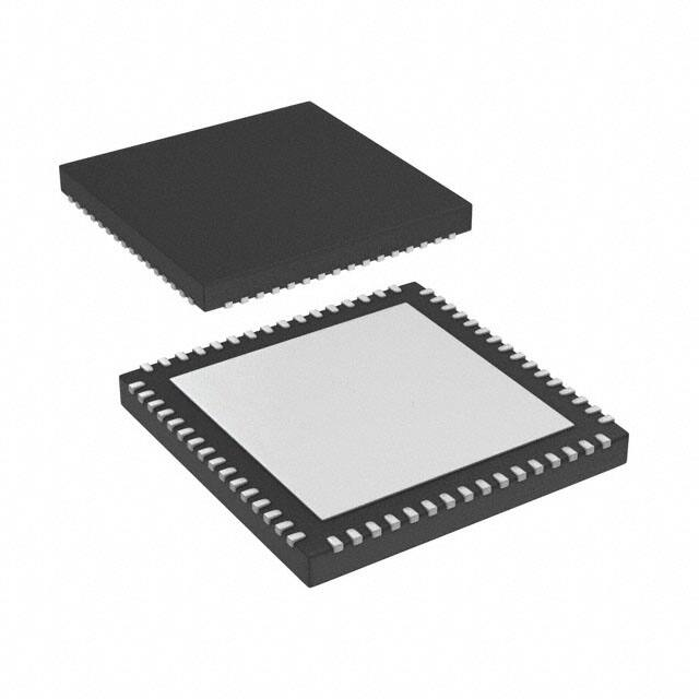
64-Pin QFN Package
The ADC driver is designed to leverage the very high
noise performance of the differential ADC at optimum
power usage levels.
The ADS8284 outputs a buffered reference signal for
level shifting of a ±4-V bipolar signal with an external
resistance divider. A Vref/2 output signal is available
to set the common-mode of a signal conditioning
circuit. The device also includes an 18-/16-/8-bit
parallel interface.
The ADS8284 is available in a 9 mm x 9 mm, 64-pin
QFN package and is characterized from -40°C to
85°C.
Device Information
(1)
DEVICE NAME
PACKAGE
BODY SIZE
ADS8284
QFN (64)
9mm x 9mm
(1) For all available packages, see the orderable addendum at
the end of the data sheet.
2 Applications
•
•
•
•
Medical Imaging/CT Scanners
Automated Test Equipment
High-Speed Data Acquisition Systems
High-Speed Closed-Loop Systems
Simplified Schematic
Analog 5 V
0.1 µF
AGND
10 µF
Ext Ref Input
0.1 µF
Micro
Controller
GPIO
GPIO
GPIO
GPIO
RD
AD[7:0]
−IN
+IN
+VA
REFIN
REFM
AGND
Analog Input
Digital 3 V
Data Bus D[17:0]
CS
AD8284
BYTE
BUS18/16
CONVST
RD
DB[17:10]
0.1 µF
BDGND
BDGND
+VBD
1
An IMPORTANT NOTICE at the end of this data sheet addresses availability, warranty, changes, use in safety-critical applications,
intellectual property matters and other important disclaimers. PRODUCTION DATA.
�Not Recommended for New Designs
ADS8284
SLAS628A – MARCH 2009 – REVISED APRIL 2014
www.ti.com
Table of Contents
1
2
3
4
5
6
Features ..................................................................
Applications ...........................................................
Description .............................................................
Revision History.....................................................
Pin Configuration and Function ...........................
Specifications.........................................................
6.1
6.2
6.3
6.4
6.5
6.6
6.7
6.8
6.9
1
1
1
2
3
6
Absolute Maximum Ratings ..................................... 6
Handling Ratings....................................................... 6
Recommended Operating Conditions....................... 6
Thermal Information .................................................. 6
Electrical Characteristics........................................... 7
Timing Requirements, 5 V ...................................... 10
Timing Requirements, 3 V ...................................... 11
Multiplexer Timing Requirements ........................... 11
Timing Diagrams ..................................................... 12
6.10 Typical Characteristics .......................................... 19
7
Device Description............................................... 30
7.1
7.2
7.3
7.4
8
Overview .................................................................
Functional Block Diagram .......................................
Feature Description.................................................
Device Functional Modes........................................
30
30
31
32
Application and Implementation ........................ 33
8.1 Application Information............................................ 33
8.2 Typical Applications ................................................ 33
9 Power Supply Recommendations...................... 36
10 Device and Documentation Support ................. 37
10.1 Trademarks ........................................................... 37
10.2 Electrostatic Discharge Caution ............................ 37
10.3 Glossary ................................................................ 37
11 Mechanical, Packaging, and Orderable
Information ........................................................... 37
4 Revision History
Changes from Original (March 2009) to Revision A
Page
•
Changed the data sheet to the new TI standard ................................................................................................................... 1
•
Added the Device Information table ....................................................................................................................................... 1
•
Added the Handling Ratings table .......................................................................................................................................... 6
•
Added Reference/2 Voltage Range to the Electrical Characteristics table ........................................................................... 8
•
Added the Power Supply Recommendations section .......................................................................................................... 36
2
Submit Documentation Feedback
Copyright © 2009–2014, Texas Instruments Incorporated
Product Folder Links: ADS8284
�Not Recommended for New Designs
ADS8284
www.ti.com
SLAS628A – MARCH 2009 – REVISED APRIL 2014
Device Comparison Table
TYPE/SPEED
500 kHz
~600 kHz
ADS8383
ADS8381
750 kHz
1 MHz
1.25 MHz
2 MHz
3 MHz
4MHz
ADS8481
18-Bit Pseudo-Diff
ADS8380 (s)
ADS8382 (s)
ADS8284
ADS8484
18-Bit Pseudo-Bipolar, Fully Diff
ADS8482
ADS8327
16-Bit Pseudo-Diff
ADS8370 (s)
ADS8371
ADS8471
ADS8328
ADS8401
ADS8411
ADS8405
ADS8410 (s)
ADS8319
ADS8318
ADS8372 (s)
ADS8472
ADS8402
ADS8412
ADS8254
ADS8406
ADS8413 (s)
ADS8422
16-Bit Pseudo-Bipolar, Fully Diff
14-Bit Pseudo-Diff
ADS7890 (s)
12-Bit Pseudo-Diff
ADS7891
ADS7886
ADS7883
ADS7881
Device Linearity
MODEL
MAXIMUM INTEGRAL
LINEARITY
(LSB)
MAXIMUM DIFFERENTIAL
LINEARITY
(LSB)
NO MISSING CODES AT
RESOLUTION
(BIT)
ADS8284lB
±2.5
+1.5/–1
18
ADS8284l
±4.5
+1.5/–1
18
5 Pin Configuration and Function
NC
BUF-REF
VCMO
+VA
AGND
REFOUT
REFIN
REFM
REFM
+VA
AGND
+VA
CS
RD
CONVST
BYTE
QFN PACKAGE
(TOP VIEW)
16 15 14 13 12 11 10 9 8
17
7 6
5 4 3
2
1
64
18
63
19
62
20
61
21
60
22
59
58
23
ADS8284
24
57
25
56
26
55
27
54
28
53
29
52
30
51
31
50
32
49
33 34 35 36 37 38 39 40 41 42 43 44 45 46 47 48
BUS18_16
+VBD
BUSY
DB0
DB1
DB2
DB3
DB4
DB5
DB6
DB7
DB8
DB9
BGND
+VBD
DB10
AUTO
C3
C2
C1
MXCLK
+VA
AGND
+VA
AGND
DB17
DB16
DB15
DB14
DB13
DB12
DB11
CH0P
CH0M
CH1P
CH1M
PD-RBUF
VEE
VCC
VCC
INP
AGND
INM
NC
CH2P
CH2M
CH3P
CH3M
Submit Documentation Feedback
Copyright © 2009–2014, Texas Instruments Incorporated
Product Folder Links: ADS8284
3
�Not Recommended for New Designs
ADS8284
SLAS628A – MARCH 2009 – REVISED APRIL 2014
www.ti.com
Pin Functions
PIN
NO
NAME
I/O
DESCRIPTION
MULTIPLEXER INPUT PINS
17
CH0P
I
Non-inverting analog input for differential multiplexer channel number 0. Device performance is optimized for 50-Ω source
impedance at this input.
18
CH0M
I
Inverting analog input for differential multiplexer channel number 0. Device performance is optimized for 50-Ω source
impedance at this input.
19
CH1P
I
Non-inverting analog input for differential multiplexer channel number 1. Device performance is optimized for 50-Ω source
impedance at this input.
20
CH1M
I
Inverting analog input for differential multiplexer channel number 1. Device performance is optimized for 50-Ω source
impedance at this input.
29
CH2P
I
Non-inverting analog input for differential multiplexer channel number 2. Device performance is optimized for 50-Ω source
impedance at this input.
30
CH2M
I
Inverting analog input for differential multiplexer channel number 2. Device performance is optimized for 50-Ω source
impedance at this input.
31
CH3P
I
Non-inverting analog input for differential multiplexer channel number 3. Device performance is optimized for 50 ohm source
impedance at this input.
32
CH3M
I
Inverting analog input for differential multiplexer channel number 3. Device performance is optimized for 50-Ω source
impedance at this input.
ADC INPUT PINS
25
INP
I
ADC Non inverting input., connect 1-nF capacitor across INP and INM
27
INM
I
ADC Inverting input, connect 1-nF capacitor across INP and INM
REFERENCE INPUT/ OUTPUT PINS
8, 9
REFM
I
Reference ground.
10
REFIN
I
Reference Input. Add 0.1-μF decoupling capacitor between REFIN and REFM.
11
REFOUT
O
Reference Output. Add 1-μF capacitor between the REFOUT pin and REFM pin when internal reference is used.
14
VCMO
O
This pin outputs REFIN/2 and can be used to set common-mode voltage of differential analog inputs.
15
BUF-REF
O
Buffered reference output. Useful to level shift bipolar signals using external resistors.
I
High on this pin powers down the reference buffer (BUF-REF).
POWER CONTROL PINS
21
PD-RBUF
MULTIPLEXER CONTROL PINS
33
AUTO
I
High level on this pin selects auto mode for multiplexer scanning. Low level selects manual mode of multiplexer scanning
34
C3
I
In auto mode (AUTO = 1) multiplexer channel selection is reset to CH0 on rising edge of MXCLK while C3 = 1. The pin is do
not care in manual mode.
35
C2
I
Acts as multiplexer address bit when AUTO = 0 (manual mode). In auto mode (AUTO = 1) C2 and C1 select the last
multiplexer channel (channel count) in the auto scan sequence.
36
C1
I
Acts as multiplexer address LSB when AUTO = 0 (manual mode). In auto mode (AUTO = 1) C2 and C1 select the last
multiplexer channel (channel count) in the auto scan sequence.
37
MXCLK
I
Multiplexer channel is selected on rising edge of MXCLK irrespective of whether it is auto or manual mode. Device BUSY
output can be connected to MXCLK so that device selects next channel at the end of every sample.
ADC DATA BUS
8-BIT BUS
42-49,
52-61
4
Data Bus
16-BIT BUS
18-BIT BUS
BYTE = 0
BYTE = 1
BYTE = 1
BYTE = 0
BYTE = 0
BYTE = 0
BUS18/16 = 0
BUS18/16 = 0
BUS18/16 = 1
BUS18/16 = 0
BUS18/16 = 1
BUS18/16 = 0
42
DB17
O
D17 (MSB)
D9
All ones
D17 (MSB)
All ones
D17 (MSB)
43
DB16
O
D16
D8
All ones
D16
All ones
D16
44
DB15
O
D15
D7
All ones
D15
All ones
D15
45
DB14
O
D14
D6
All ones
D14
All ones
D14
46
DB13
O
D13
D5
All ones
D13
All ones
D13
47
DB12
O
D12
D4
All ones
D12
All ones
D12
48
DB11
O
D11
D3
D1
D11
All ones
D11
49
DB10
O
D10
D2
D0 (LSB)
D10
All ones
D10
52
DB9
O
D9
All ones
All ones
D9
All ones
D9
53
DB8
O
D8
All ones
All ones
D8
All ones
D8
54
DB7
O
D7
All ones
All ones
D7
All ones
D7
55
DB6
O
D6
All ones
All ones
D6
All ones
D6
56
DB5
O
D5
All ones
All ones
D5
All ones
D5
Submit Documentation Feedback
Copyright © 2009–2014, Texas Instruments Incorporated
Product Folder Links: ADS8284
�Not Recommended for New Designs
ADS8284
www.ti.com
SLAS628A – MARCH 2009 – REVISED APRIL 2014
Pin Functions (continued)
PIN
I/O
DESCRIPTION
NO
NAME
57
DB4
O
D4
All ones
All ones
D4
All ones
D4
58
DB3
O
D3
All ones
All ones
D3
D1
D3
59
DB2
O
D2
All ones
All ones
D2
D0 (LSB)
D2
60
DB1
O
D1
All ones
All ones
D1
All ones
D1
61
DB0
O
D0 (LSB)
All ones
All ones
D0 (LSB)
All ones
D0 (LSB)
ADC CONTROL PINS
62
BUSY
O
Status output. This pin is held high when device is converting.
64
BUS18_16
I
Bus size select input. Used for selecting 18-bit or 16-bit wide bus transfer. Refer to ADC DATA BUS description above.
1
BYTE
I
Byte Select Input. Used for 8-bit bus reading. Refer to ADC DATA BUS description above.
2
CONVST
I
Convert start. This input is active low and can act independent of the CS input.
3
RD
I
Synchronization pulse for the parallel output.
4
CS
I
Chip select.
DEVICE POWER SUPPLIES
22
VEE
Negative supply for OPA (OP1, OP2)
23, 24
VCC
Positive supply for OPA (OP1, OP2, BUF-REF)
5, 7,
13, 38,
40
+VA
Analog power supply.
6, 12,
26, 39,
41
AGND
Analog ground.
50, 63
+VBD
Digital power supply for ADC bus.
51
BGND
Digital ground for ADC bus interface digital supply.
NOT CONNECTED PINS
16, 28
NC
No connection.
Submit Documentation Feedback
Copyright © 2009–2014, Texas Instruments Incorporated
Product Folder Links: ADS8284
5
�Not Recommended for New Designs
ADS8284
SLAS628A – MARCH 2009 – REVISED APRIL 2014
www.ti.com
6 Specifications
6.1 Absolute Maximum Ratings (1)
over operating free-air temperature range (unless otherwise noted)
MIN
MAX
UNIT
VEE–0.3
VCC + 0.3
V
VCC to VEE
-0.3
18
V
+VA to AGND
–0.3
7
V
+VBD to BDGND
–0.3
7
V
ADC control digital input voltage to GND
–0.3
(+VBD + 0.3)
V
ADC control digital output to GND
–0.3
(+VBD + 0.3)
V
Multiplexer control digital input voltage to GND
–0.3
(+VA + 0.3)
V
Power control digital input voltage to GND
–0.3
(+VCC + 0.3)
V
Operating temperature range
–40
85
°C
150
°C
CH(i) to AGND (both P and M inputs)
Junction temperature (TJmax)
(1)
Stresses beyond those listed under absolute maximum ratings may cause permanent damage to the device. These are stress ratings
only, and functional operation of the device at these or any other conditions beyond those indicated under recommended operating
conditions is not implied. Exposure to absolute-maximum-rated conditions for extended periods may affect device reliability.
6.2 Handling Ratings
Tstg
Storage temperature range
V(ESD)
(1)
(2)
Electrostatic discharge
Human body model (HBM), per ANSI/ESDA/JEDEC JS-001, all
pins (1)
Charged device model (CDM), per JEDEC specification
JESD22-C101, all pins (2)
MIN
MAX
UNIT
–65
150
°C
–2
2
kV
–500
500
V
JEDEC document JEP155 states that 500-V HBM allows safe manufacturing with a standard ESD control process.
JEDEC document JEP157 states that 250-V CDM allows safe manufacturing with a standard ESD control process.
6.3 Recommended Operating Conditions
over operating free-air temperature range (unless otherwise noted)
MIN
Analog Input at Multiplexer Inputs
CHxP, CHxM
Digital Supply Voltage
+VBD
Analog Supply Voltage
NOM
0
MAX
UNIT
VREF
V
2.7
3.3
5.25
V
+VA
4.75
5
5.25
V
Positive Supply Voltage for OPA
VCC
4.75
5
7.5
V
Negative Supply Voltage for OPA
VEE
–7.5
–5
–3
V
6.4 Thermal Information
THERMAL METRIC (1)
RCG
64 PINS
RθJA
Junction-to-ambient thermal resistance
24.0
RθJC(top)
Junction-to-case(top) thermal resistance
7.8
RθJB
Junction-to-board thermal resistance
3.2
ψJT
Junction-to-top characterization parameter
0.1
ψJB
Junction-to-board characterization parameter
3.2
RθJC(bottom)
Junction-to-case(bottom) thermal resistance
n/a
(1)
6
UNIT
°C/W
For more information about traditional and new thermal metrics, see the IC Package Thermal Metrics application report, SPRA953.
Submit Documentation Feedback
Copyright © 2009–2014, Texas Instruments Incorporated
Product Folder Links: ADS8284
�Not Recommended for New Designs
ADS8284
www.ti.com
SLAS628A – MARCH 2009 – REVISED APRIL 2014
6.5 Electrical Characteristics
TA = –40°C to 85°C, VCC = 5 V, VEE = –5 V, +VA = 5 V, +VBD = 5 V or 3.3 V, Vref = 4 V, fSAMPLE = 1 MSPS (unless
otherwise noted)
PARAMETER
TEST CONDITIONS
MIN
TYP
MAX
UNIT
ANALOG INPUT
Full-scale input voltage at multiplexer input (1)
CH(i)P–CH(i)M
–Vref
Vref
V
Absolute input range at multiplexer input
CH (i)
–0.2
Vref + 0.2
V
(Vref)/2
+ 0.2
V
[CH(i)P + CH(i)M] /2
Input common-mode voltage
(Vref)/2
– 0.2
(Vref)/2
SYSTEM PERFORMANCE
Resolution
18
No missing codes
Integral linearity
(2)
Differential linearity
Offset error
Gain error (4)
ADS8284IB
18
ADS8284I
18
Bits
Bits
ADS8284IB
–2.5
±1.25
2.5
ADS8284I
–4.5
±1.5
4.5
–1
±0.6
1.5
–1
±0.6
1.5
ADS8284IB
–0.5
±0.05
0.5
ADS8284I
–0.5
±0.05
0.5
–0.1
±0.025
0.1
–0.1
±0.025
0.1
ADS8284IB
ADS8284I
ADS8284IB
ADS8284I
DC power supply rejection ratio
At 18-bit level
External reference
At 3FFF0H output code. For +VA or VCC, VEE
variation of 0.5 V individually
80
LSB
(3)
LSB (3)
mV
%FS
dB
SAMPLING DYNAMICS
Conversion time
Acquisition time
+VBD = 5 V
625
650
ns
+VDB = 3 V
625
650
ns
+VBD = 5 V
320
350
+VDB = 3 V
320
350
Maximum throughput rate
ns
1.0
MHz
Aperture delay
4
ns
Aperture jitter
5
ps
For ADC only
150
ns
For OPA (OP1, OP2) + mux
700
For ADC only
150
Settling time to 0.5 LSB
Over voltage recovery
ns
DYNAMIC CHARACTERISTICS
ADS8284I
ADS8284IB
Total harmonic distortion
(THD) (5)
ADS8284I
ADS8284IB
ADS8284I
ADS8284IB
ADS8284I
ADS8284IB
Signal-to-noise ratio (SNR)
ADS8284I
ADS8284IB
ADS8284I
ADS8284IB
(1)
(2)
(3)
(4)
(5)
–119
VIN = 4 Vpp at 2 kHz
–119
–105
VIN = 4 Vpp at 10 kHz
–105
–100
VIN = 4 Vpp at 100 kHz,
LoPWR = 0
VIN = 4 Vpp at 2 kHz
VIN = 4 Vpp at 10 kHz
VIN = 4 Vpp at 100 kHz,
LoPWR = 0
–100
98.4
97.5
98.4
98
98
95
97
dB
dB
dB
dB
dB
dB
Ideal input span, does not include gain or offset error.
This is endpoint INL, not best fit.
LSB means least significant bit.
Calculated on the first nine harmonics of the input frequency.
Measured relative to acutal measured reference.
Submit Documentation Feedback
Copyright © 2009–2014, Texas Instruments Incorporated
Product Folder Links: ADS8284
7
�Not Recommended for New Designs
ADS8284
SLAS628A – MARCH 2009 – REVISED APRIL 2014
www.ti.com
Electrical Characteristics (continued)
TA = –40°C to 85°C, VCC = 5 V, VEE = –5 V, +VA = 5 V, +VBD = 5 V or 3.3 V, Vref = 4 V, fSAMPLE = 1 MSPS (unless
otherwise noted)
PARAMETER
ADS8284I
ADS8284IB
Signal-to-noise + distortion
(SINAD)
ADS8284I
ADS8284IB
ADS8284I
ADS8284IB
ADS8284I
ADS8284IB
ADS8284I
Spurious free dynamic
range (SFDR)
ADS8284IB
ADS8284I
ADS8284IB
TEST CONDITIONS
MIN
TYP
MAX
98.3
VIN = 4 Vpp at 2 kHz
dB
98.3
97.2
VIN = 4 Vpp at 10 kHz
dB
97.2
93.8
VIN = 4 Vpp at 100 kHz,
LoPWR = 0
dB
95.23
121
VIN = 4 Vpp at 2 kHz
dB
121
106
VIN = 4 Vpp at 10 kHz
dB
106
101
VIN = 4 Vpp at 100 kHz,
LoPWR = 0
dB
101
–3dB small signal bandwidth
UNIT
8
MHz
VOLTAGE REFERENCE INPUT (REFIN)
Reference voltage at REFIN, Vref
Reference input current
3.0
(6)
4.096
+VA – 0.8
V
1
1
μA
120
ms
4.096
4.111
V
10
μA
INTERNAL REFERENCE OUTPUT (REFOUT)
Internal reference start-up time
From 95% (+VA), with 1-μF storage capacitor
Reference voltage range, Vref
4.081
Source current
Static load
Line regulation
+VA = 4.75 V to 5.25 V
60
μV
Drift
IO = 0
±6
PPM/°C
REFIN = 4 V, at 85°C
70
mA
BUFFERED REFERENCE OUTPUT (BUF-REF)
Output current
REFERENCE/2 OUTPUT (VCMO)
Reference/2 Voltage Range
At No Load on VCMO
Output current
REFIN = 4 V, at +85°C
1.938
2.048
2.158
V
μA
50
ANALOG MULTIPLEXER
Number of channels
4
Channel to channel crosstalk
100 kHz i/p
–95
Channel selection
Auto sequencer with selection of channel count or
manual selection through control lines
dB
DIGITAL INPUT-OUTPUT
ADC CONTROL PINS
Logic Family-CMOS
Logic level
VIH
IIH = 5 μA
VIL
IIL = 5 μA
VOH
IOH = 2 TTL loads
VOL
IOL = 2 TTL loads
+V BD–1
+VBD + 0.3
V
0.3
0.8
V
+VBD–0.6
+VBD
V
0
0.4
V
MULTIPLEXER CONTROL PINS
Logic Family - CMOS
Logic level
IIH
IIH = 5 μA
2.3
+VA +0.3
V
IIL
IIL = 5 μA
–0.3
0.8
V
VIH
IIH = 5 μA
2.3
+VA +0.3
V
VIL
IIL = 5 μA
–0.3
0.8
V
POWER CONTROL PINS
Logic Family - CMOS
Logic level
(6)
8
Can vary ±20%
Submit Documentation Feedback
Copyright © 2009–2014, Texas Instruments Incorporated
Product Folder Links: ADS8284
�Not Recommended for New Designs
ADS8284
www.ti.com
SLAS628A – MARCH 2009 – REVISED APRIL 2014
Electrical Characteristics (continued)
TA = –40°C to 85°C, VCC = 5 V, VEE = –5 V, +VA = 5 V, +VBD = 5 V or 3.3 V, Vref = 4 V, fSAMPLE = 1 MSPS (unless
otherwise noted)
PARAMETER
TEST CONDITIONS
POWER SUPPLY REQUIREMENTS
+VBD
Power supply voltage
MIN
TYP
MAX
UNIT
2.7
3.3
5.25
V
+VA
4.75
5
5.25
V
VCC
4.75
5
7.5
V
VEE
–7.5
–5
–3
V
ADC driver positive supply (VCC) current (for OP1 and
OP2 together)
VCC = +5, VEE = -5V, CH0 - CH3 p and m inputs
shorted to each other and connected to 2V
11.65
mA
ADC driver negative supply ( VEE) current (for OP1 and VCC= +5V, CH0 - CH3 p and m inputs shorted to
OP1 together)
each other and connected to 2V
9.6
mA
+VA supply current, 1-MHz sample rate
45
Reference buffer (BUF-REF) supply current (VCC to
GND)
VCC= +5, PD-RBUF = 0, Quiescent current
VCC = 5, PD-RBUF = 1 (7)
50
mA
8
mA
10
μA
TEMPERATURE RANGE
Operating free-air
(7)
–40
85
°C
PD-RBUF = 1 powers down the reference buffer (BUF-REF), note that it does not 3-state the BUF-REF output.
Submit Documentation Feedback
Copyright © 2009–2014, Texas Instruments Incorporated
Product Folder Links: ADS8284
9
�Not Recommended for New Designs
ADS8284
SLAS628A – MARCH 2009 – REVISED APRIL 2014
www.ti.com
6.6 Timing Requirements, 5 V
All specifications typical at –40°C to 85°C, +VA = +VBD = 5 V
(1) (2) (3)
PARAMETER
MIN
TYP
MAX
UNIT
650
ns
t(CONV)
Conversion time
t(ACQ)
Acquisition time
t(HOLD)
Sample capacitor hold time
25
ns
tpd1
CONVST low to BUSY high
40
ns
tpd2
Propagation delay time, end of conversion to BUSY low
15
ns
tpd3
Propagation delay time, start of convert state to rising edge of BUSY
15
ns
tw1
Pulse duration, CONVST low
40
ns
tsu1
Setup time, CS low to CONVST low
20
ns
tw2
Pulse duration, CONVST high
20
320
CONVST falling edge jitter
ns
ns
10
t(ACQ)min
ps
tw3
Pulse duration, BUSY signal low
tw4
Pulse duration, BUSY signal high
th1
Hold time, first data bus transition (RD low, or CS low for read cycle, or BYTE or
BUS18/16 input changes) after CONVST low
td1
tsu2
tw5
Pulse duration, RD low
ten
Enable time, RD low (or CS low for read cycle) to data valid
td2
Delay time, data hold from RD high
td3
Delay time, BUS18/16 or BYTE rising edge or falling edge to data valid
10
tw6
Pulse duration, RD high
20
ns
tw7
Pulse duration, CS high
20
ns
th2
Hold time, last RD (or CS for read cycle ) rising edge to CONVST falling edge
50
ns
tpd4
Propagation delay time, BUSY falling edge to next RD (or CS for read cycle) falling
edge
0
ns
td4
Delay time, BYTE edge to BUS18/16 edge skew
0
ns
tsu3
Setup time, BYTE or BUS18/16 transition to RD falling edge
10
ns
th3
Hold time, BYTE or BUS18/16 transition to RD falling edge
10
tdis
Disable time, RD high (CS high for read cycle) to 3-stated data bus
td5
Delay time, BUSY low to MSB data valid delay
td6
Delay time, CS rising edge to BUSY falling edge
50
ns
td7
Delay time, BUSY falling edge to CS rising edge
50
ns
tsu5
BYTE transition setup time, from BYTE transition to next BYTE transition, or BUS18/16
transition setup time, from BUS18/16 to next BUS18/16.
50
ns
10
ns
40
ns
Delay time, CS low to RD low
0
ns
Setup time, RD high to CS high
0
ns
50
ns
20
5
tsu(ABORT) Setup time from the falling edge of CONVST (used to start the valid conversion) to the
next falling edge of CONVST (when CS = 0 and CONVST are used to abort) or to the
next falling edge of CS (when CS is used to abort).
(1)
(2)
(3)
ns
650
60
ns
ns
20
ns
ns
20
ns
0
ns
550
ns
All input signals are specified with tr = tf = 5 ns (10% to 90% of +VBD) and timed from a voltage level of (VIL + VIH)/2.
See timing diagrams.
All timing are measured with 20 pF equivalent loads on all data bits and BUSY pins.
Submit Documentation Feedback
Copyright © 2009–2014, Texas Instruments Incorporated
Product Folder Links: ADS8284
�Not Recommended for New Designs
ADS8284
www.ti.com
SLAS628A – MARCH 2009 – REVISED APRIL 2014
6.7 Timing Requirements, 3 V
All specifications typical at –40°C to 85°C, +VA = 5 V +VBD = 3 V
(1) (2) (3)
PARAMETER
MIN
TYP
MAX
UNIT
650
ns
t(CONV)
Conversion time
t(ACQ)
Acquisition time
t(HOLD)
Sample capacitor hold time
25
ns
tpd1
CONVST low to BUSY high
40
ns
tpd2
Propagation delay time, end of conversion to BUSY low
25
ns
tpd3
Propagation delay time, start of convert state to rising edge of BUSY
25
ns
tw1
Pulse duration, CONVST low
40
ns
tsu1
Setup time, CS low to CONVST low
20
ns
tw2
Pulse duration, CONVST high
20
320
ns
ns
CONVST falling edge jitter
10
t(ACQ)min
ps
tw3
Pulse duration, BUSY signal low
tw4
Pulse duration, BUSY signal high
th1
Hold time, first data bus transition (RD low, or CS low for read cycle, or BYTE or
BUS18/16 input changes) after CONVST low
td1
tsu2
tw5
Pulse duration, RD low
ten
Enable time, RD low (or CS low for read cycle) to data valid
td2
Delay time, data hold from RD high
td3
Delay time, BUS18/16 or BYTE rising edge or falling edge to data valid
10
tw6
Pulse duration, RD high
20
ns
tw7
Pulse duration, CS high
20
ns
th2
Hold time, last RD (or CS for read cycle ) rising edge to CONVST falling edge
50
ns
tpd4
Propagation delay time, BUSY falling edge to next RD (or CS for read cycle) falling
edge
0
ns
td4
Delay time, BYTE edge to BUS18/16 edge skew
0
ns
tsu3
Setup time, BYTE or BUS18/16 transition to RD falling edge
10
ns
th3
Hold time, BYTE or BUS18/16 transition to RD falling edge
10
tdis
Disable time, RD high (CS high for read cycle) to 3-stated data bus
td5
Delay time, BUSY low to MSB data valid delay
td6
Delay time, CS rising edge to BUSY falling edge
50
ns
td7
Delay time, BUSY falling edge to CS rising edge
50
ns
tsu5
BYTE transition setup time, from BYTE transition to next BYTE transition, or BUS18/16
transition setup time, from BUS18/16 to next BUS18/16.
50
ns
ns
40
ns
Delay time, CS low to RD low
0
ns
Setup time, RD high to CS high
0
ns
50
ns
30
5
tsu(ABORT) Setup time from the falling edge of CONVST (used to start the valid conversion) to the
next falling edge of CONVST (when CS = 0 and CONVST are used to abort) or to the
next falling edge of CS (when CS is used to abort).
(1)
(2)
(3)
ns
650
ns
ns
30
ns
ns
70
30
ns
0
ns
550
ns
MAX
UNIT
600
ns
All input signals are specified with tr = tf = 5 ns (10% to 90% of +VBD) and timed from a voltage level of (VIL + VIH)/2.
See timing diagrams.
All timing are measured with 20-pF equivalent loads on all data bits and BUSY pins.
6.8 Multiplexer Timing Requirements
VCC = 4.75 V to 7.5 V, VEE = -3 V to -7.5 V
MIN
tsu6
Setup time C1, C2 or C3 to MXCLK rising edge
td8
Multiplexer and driver settle time ( from MXCLK rising edge to CONVST falling edge)
TYP
600
Submit Documentation Feedback
Copyright © 2009–2014, Texas Instruments Incorporated
Product Folder Links: ADS8284
ns
11
�Not Recommended for New Designs
ADS8284
SLAS628A – MARCH 2009 – REVISED APRIL 2014
www.ti.com
6.9 Timing Diagrams
The ADS8284 is analog system-on-chip (SoC) device. The device includes a multiplexer, a differential
input/differential output ADC driver and differential input high-performance ADC, an additional internal reference,
a buffered reference output, and a REF/2 output.
Figure 1 shows the basic operation of the device (including all elements). Subsequent sections describe the
detailed timings of the individual blocks of the device (primarily the multiplexer and ADC).
m-1
m
m+1
m+2
CONVST
BUSY
SELECTED
CHANNEL
Ch (n-1)
Ch (n)
Ch (n+1)
Ch (n+2)
Ch (n+3)
INP
Vref V
ADC differential
input assuming
alternate channels
have+Vref & -Vref
differential input
SAMPLE,
(Vinp- Vinm)
DB17 - DB0
Parallel o/ p bus
0V
INM
S(m-1)
-Vref
Ch (n-2)
S(m)
+Vref
Ch (n-1)
S(m+1)
-Vref
Ch (n)
S(m+2)
+Vref
Ch (n+1)
Figure 1. Device Operation
As shown in the diagram, the device can be controlled with only one (CONVST) digital input. On the falling edge
of CONVST, the BUSY output of the device goes high. A high level on BUSY indicates the device has sampled
the signal and it is converting the sample into its digital equivalent. After the conversion is complete, the BUSY
output falls to a logic low level and the device output data corresponding to the recently converted sample is
available for reading.
It is recommended (not mandatory) to short the BUSY output of the device to the MXCLK input. The device
selects a new channel at every rising edge of MXCLK. The multiplexer is differential. The multiplexer and ADC
driver are designed to settle to the 18-bit level before sampling; even at the maximum conversion speed.
ADC control and timing: The timing diagrams in this section describe ADC operation; multiplexer operation is
described in a later section.
12
Submit Documentation Feedback
Copyright © 2009–2014, Texas Instruments Incorporated
Product Folder Links: ADS8284
�Not Recommended for New Designs
ADS8284
www.ti.com
SLAS628A – MARCH 2009 – REVISED APRIL 2014
Timing Diagrams (continued)
tw2
tw1
CONVST
tpd1
tpd2
tw4
tw3
BUSY
tsu1
CS
tpd3
tw7
td7
td6
CONVERT†
t(CONV)
t(CONV)
t(HOLD)
SAMPLING†
(When CS Toggle)
t(ACQ)
tsu(ABORT)
tsu(ABORT)
BYTE
tsu5
th1
BUS 18/16
tsu5
tsu2
tpd4
th2
td1
RD
tdis
ten
DB[17:12]
Hi−Z
D[17:12]
Hi−Z
D[9:4]
MSB
DB[11:10]
DB[9:0]
†Signal
Hi−Z
Hi−Z
D[11:10]
D[3:2]
D[1:0]
Hi−Z
Hi−Z
D[9:0]
internal to device
Figure 2. Timing for Conversion and Acquisition Cycles with CS and RD Toggling
Submit Documentation Feedback
Copyright © 2009–2014, Texas Instruments Incorporated
Product Folder Links: ADS8284
13
�Not Recommended for New Designs
ADS8284
SLAS628A – MARCH 2009 – REVISED APRIL 2014
www.ti.com
Timing Diagrams (continued)
tw1
tw2
CONVST
tpd1
tpd2
tw4
tw3
BUSY
tsu1
tw7
td7
CS
tpd3
td6
CONVERT†
t(CONV)
t(CONV)
t(HOLD)
SAMPLING†
(When CS Toggle)
t(ACQ)
tsu(ABORT)
tsu(ABORT)
BYTE
tsu5
th1
BUS 18/16
tpd4
th2
RD = 0
ten
DB[17:12]
DB[11:10]
DB[9:0]
†Signal
ten
tdis
Previous
Hi−Z D[17:12]
Hi−Z
Hi−Z
Previous
D[11:10]
Previous
D [9:0]
Hi−Z
Hi−Z
Hi−Z
tdis
ten
MSB
D[17:12]
D[11:10]
D[9:0]
Hi−Z
D[9:4]
D[3:2]
D[1:0]
Hi−Z
Hi−Z
Repeated
D[17:12]
Repeated
D[11:10]
Repeated
D [9:0]
internal to device
Figure 3. Timing for Conversion and Acquisition Cycles with CS Toggling, RD Tied to BDGND
14
Submit Documentation Feedback
Copyright © 2009–2014, Texas Instruments Incorporated
Product Folder Links: ADS8284
�Not Recommended for New Designs
ADS8284
www.ti.com
SLAS628A – MARCH 2009 – REVISED APRIL 2014
Timing Diagrams (continued)
tw1
tw2
CONVST
tpd1
tpd2
tw4
tw3
BUSY
CS = 0
CONVERT†
t(CONV)
t(CONV)
t(HOLD)
t(ACQ)
SAMPLING†
(When CS = 0)
tsu(ABORT)
tsu(ABORT)
BYTE
tsu5
th1
BUS 18/16
tsu5
tpd4
th2
RD
tdis
ten
MSB
DB[17:12]
DB[11:10]
DB[9:0]
†Signal
Hi−Z
Hi−Z
Hi−Z
D[17:12]
D[9:4]
D[11:10]
D[3:2]
D[9:0]
Hi−Z
D[1:0]
Hi−Z
Hi−Z
internal to device
Figure 4. Timing for Conversion and Acquisition Cycles With CS Tied to BDGND, RD Toggling
Submit Documentation Feedback
Copyright © 2009–2014, Texas Instruments Incorporated
Product Folder Links: ADS8284
15
�Not Recommended for New Designs
ADS8284
SLAS628A – MARCH 2009 – REVISED APRIL 2014
www.ti.com
Timing Diagrams (continued)
tw2
tw1
CONVST
tpd1
tw4
tpd2
tw3
BUSY
CS = 0
CONVERT†
t(CONV)
t(CONV)
tpd3
tpd3
t(HOLD)
t(HOLD)
t(ACQ)
SAMPLING†
(When CS = 0)
tsu(ABORT)
tsu(ABORT)
BYTE
tsu5
tsu5
BUS 18/16
tsu5
tsu5
th1
th1
RD = 0
td5
DB[17:12]
DB[11:10]
D[17:12]
Previous LSB
DB[9:0]
†Signal
D[11:10]
Next D[17:12]
D[9:4]
D[3:2]
D[9:0]
D[1:0]
Next D[11:10]
Next D[9:0]
internal to device
Figure 5. Timing for Conversion and Acquisition Cycles With CS and RD Tied to BDGND - Auto Read
16
Submit Documentation Feedback
Copyright © 2009–2014, Texas Instruments Incorporated
Product Folder Links: ADS8284
�Not Recommended for New Designs
ADS8284
www.ti.com
SLAS628A – MARCH 2009 – REVISED APRIL 2014
Timing Diagrams (continued)
CS
RD
BYTE
tsu5
BUS 18/16
ten
ten
DB[17:0]
tdis
Hi−Z
Valid
Hi−Z
td3
tdis
td3
Valid
Valid
Hi−Z
Figure 6. Detailed Timing for Read Cycles
Multiplexer: The multiplexer has two modes of sequencing namely auto sequencing and manual sequencing.
Multiplexer mode selection and operation is controlled with the AUTO, C1, C2, C3, and MXCLK pin.
Auto sequencing: A logic one level on the AUTO pin selects auto sequencing mode. It is possible to select the
number of channels to be scanned (always starting from channel zero) in auto sequencing mode. Pins C1 and
C2 select the channel count (last channel in the auto sequence).
On every rising edge of MXCLK while C3 is at the logic zero level, the next higher channel (in ascending order)
is selected. Channel selection rolls over to channel zero on the rising edge of MXCLK after channel selection
reaches the channel count (last channel in the auto sequence selected by pins C1and C2).
Any time during the sequence the channel sequence can be reset to channel zero. A rising edge on MXCLK
while C3 is at the logic one level resets channel selection to channel zero.
Table 1. Channel Selection in Auto Mode
CHANNEL COUNT PINS
CLOCK PIN
LAST CHANNEL IN SEQUENCE
CHANNEL SEQUENCE
C3
C2
C1
MXCLK
0
0
0
↑
0
0,0,0,0..
0
0
1
↑
1
0,1,0,1,..
0
1
0
↑
2
0,1,2,0,1,2,0…
0
1
1
↑
3
0,1,2,3,0,1,2,3,0…
1
X
X
↑
X
n → 0 (channel reset to zero)
Submit Documentation Feedback
Copyright © 2009–2014, Texas Instruments Incorporated
Product Folder Links: ADS8284
17
�Not Recommended for New Designs
ADS8284
SLAS628A – MARCH 2009 – REVISED APRIL 2014
www.ti.com
MXCLK
C3
tsu6
C2
C1
Selected
Channel
Ch 0
Ch 1
Ch 0
Ch 1
Ch 0
Ch 0
Ch 1
Ch 2
AUTO = 1, device operation in auto mode
Figure 7. Multiplexer Auto Mode Timing Diagram
Manual sequencing: A logic zero level on the AUTO pin selects manual sequencing mode. Pins C1and C2 set
the channel address. On the rising edge of MXCLK, the addressed channel is connected to the ADC driver input.
Table 2. Channel Selection in Manual Mode
MODE
CHANNEL ADDRESS PINS
CLOCK PIN
CHANNEL
AUTO
C3
C2
C1
MXCLK
0
X
0
0
↑
0
0
X
0
1
↑
1
0
X
1
0
↑
2
0
X
1
1
↑
3
MXCLK
C2
C1
Selected
Channel
tsu6
Ch 0
Ch 3
Ch 1
Ch 2
Ch 0
Ch 1
Ch 3
Ch 2
AUTO = 0, device operation in manual mode
Figure 8. Multiplexer Manual Mode Timing Diagram
18
Submit Documentation Feedback
Copyright © 2009–2014, Texas Instruments Incorporated
Product Folder Links: ADS8284
�Not Recommended for New Designs
ADS8284
www.ti.com
SLAS628A – MARCH 2009 – REVISED APRIL 2014
6.10 Typical Characteristics
20000
18000
16000
14000
3000
18230
TA = 25°C,
17372
Vref = 4.096 V,
VCC = 6 V,
VEE = -6 V,
+VA = 5 V
12000
2850
TA = 25°C,
Vref = 4.096 V,
2325 VCC = 6 V,
VEE = -6 V,
+VA = 5 V
2500
2028
2000
10533
10293
1500
10000
1194
8000
6000
3999
500
Figure 9. DC Histogram
(CH0 without mux switching)
4.098
Reference Voltage - V
4.096
4.0955
131049
131047
131045
131043
131044
4.09718
4.09717
4.09716
4.09715
4.09714
4.095
-40
-25 -10
5
20
35
50
65
4.09713
4.75
80
4.85
TA - Free-Air Temperature - °C
Figure 11. Internal Reference Voltage vs
Free-air Temperature
4.95
5.05
5.15
Supply Voltage - V
5.25
Figure 12. Internal Reference Voltage vs Sl Voltage
44
44
+VA = 5 V,
Throughput = 1 MSPS
43.75
IA - Supply Current - mA
Supply Current - mA
131041
TA = 25°C
4.09719
4.0965
43.5
43.25
43
42.75
42.5
42.25
-40
131042
4.0972
+VA = 5 V,
+VBD = 5 V
4.097
43.75
7 2
131048
56
Figure 10. DC Histogram
(CH0 with mux switching, CH 0-1-0)
4.0975
Reference Voltage - V
131039
0
2 44
131038
131047
131048
131045
131046
131043
131044
131041
131042
131039
131040
131049
118 8
4 86
280
234
777
131040
748
131050
2000
131046
3368
4000
0
978
1000
TA = 25°C,
Throughput = 1 MSPS
43.5
43.25
43
42.75
42.5
42.25
-20
0
20
40
60
TA - Free-Air Temperature - °C
42
4.70
80
Figure 13. Analog Voltage (+VA) Supply Current (IA) vs
Free-air Temperature
4.80
4.90
5
5.10 5.20
+VA - Analog Voltage - V
5.30 5.40
Figure 14. Supply Current (IA) vs Analog Voltage (+VA)
Submit Documentation Feedback
Copyright © 2009–2014, Texas Instruments Incorporated
Product Folder Links: ADS8284
19
�Not Recommended for New Designs
ADS8284
SLAS628A – MARCH 2009 – REVISED APRIL 2014
www.ti.com
Typical Characteristics (continued)
14
46
+VA = 5 V,
+VBD = 5 V,
TA = 25°C,
Vref = 4.096 V
ICC - Supply Current - mA
Supply Current - mA
45
VCC = 6 V,
VEE = -6 V
13.5
44
43
42
41
13
12.5
12
11.5
11
10.5
10
40
9.5
39
250
750
500
Sample Rate - KSPS
9
-40
1000
Figure 15. Analog Supply Current vs Sample Rate
80
Figure 16. OPA Positive Supply Current (ICC) vs
Free-air Temperature
11
12
TA = 25°C,
VEE = -6 V
11.9
VCC = 6 V,
VEE = -6 V
10.5
11.8
IEE - Supply Current - mA
ICC - Supply Current - mA
-20
0
20
40
60
TA - Free-Air Temperature - °C
11.7
11.6
11.5
11.4
11.3
11.2
10
9.5
9
8.5
11.1
8
-40
11
5
6
7
VCC+ - Supply Voltage - V
4
8
Figure 17. OPA Positive Supply Current (ICC) vs
OPA Positive Supply Voltage (+VCC)
1
DNL - Differential Non Linearity - LSB
TA = 25°C,
VCC = 6 V
IEE - Supply Current - mA
80
Figure 18. OPA -VE Supply Current (IEE) vs
Free-air Temperature
9.65
9.6
9.55
9.5
9.45
-8
-7
-6
-5
-4
-3
VEE - Voltage Supply - V
0.75
0.5
Channel = 0
Vref = 4.096 V,
VCC = 6 V,
VEE = -6 V,
+VA = 5 V,
Throughput = 1 MSPS
0.25
0
-0.25
-0.5
-0.75
-1
-40
9.4
-2
-20
0
20
40
60
80
TA - Free-Air Temperature - °C
Figure 19. OPA Negative Supply Current (IEE) vs
OPA Negative Supply Voltage (-VEE)
20
-20
0
20
40
60
TA - Free-Air Temperature - °C
Figure 20. Differential Nonlinearity vs Free-air Temperature
Submit Documentation Feedback
Copyright © 2009–2014, Texas Instruments Incorporated
Product Folder Links: ADS8284
�Not Recommended for New Designs
ADS8284
www.ti.com
SLAS628A – MARCH 2009 – REVISED APRIL 2014
Typical Characteristics (continued)
1
DNL - Differential Non Linearity - LSB
DNL - Differential Non Linearity - LSB
1
0.75
0.5
Channel = 0
Vref = 4.096 V,
TA = 25°C,
VCC = 6 V,
Throughput = 1 MSPS
0.25
0
-0.25
-0.5
-0.75
-1
4.7
4.8
4.9
5
5.1
5.2
5.3
0.75
0.5
0
-0.25
-0.5
-0.75
-1
3
5.4
Channel = 0
TA = 25°C,
VCC = 6 V,
+VA = 5 V,
Throughput = 1 MSPS
0.25
3.2
+VA - Analog Supply - V
1
1
0.8
0.8
0.6
0.4
Channel = 0
Vref = 4.096 V,
TA = 25°C,
+VA = 5 V,
-7.5 V < VEE < -2.5 V,
Throughput = 1 MSPS
0.2
0
-0.2
-0.4
-0.6
-0.8
-1
4
4.5
5
5.5
6
6.5
7
7.5
VCC - Supply Voltage - V
0.4
0
-0.2
-0.4
-0.6
-0.8
2
2
1.5
1.5
1
0.5
0
-0.5
Channel = 0
Vref = 4.096 V,
VCC = 6 V,
VEE = -6 V,
+VA = 5 V,
Throughput = 1 MSPS
-1
-1.5
-2
-40
-20
0
20
40
60
TA - Free-Air Temperature - °C
TA = 25°C,
Vref = 4.096 V,
VCC = 6 V,
VEE = -6 V,
+VA = 5 V,
Throughput = 1 MSPS
0.2
1
2
Multiplexer Channels
3
Figure 24. Differential Nonlinearity vs Multiplexer Channels
INL - Integral Non Linearity - LSB
INL - Integral Non Linearity - LSB
0.6
-1
0
8
Figure 23. Differential Nonlinearity vs
OPA Supply Voltage (VCC)
4.4
Figure 22. Differential Nonlinearity vs Reference Voltage
DNL - Differential Non Linearity - LSB
DNL - Differential Non Linearity - LSB
Figure 21. Differential Nonlinearity vs
Analog Supply Voltage (+VA)
3.4
3.6
3.8
4
4.2
VREF - Reference Voltage - V
1
Channel = 0
TA = 25°C
Vref = 4.096 V,
VCC = 6 V,
VEE = -6 V,
Throughput = 1 MSPS
0.5
0
-0.5
-1
-1.5
-2
4.7
80
Figure 25. Integral Nonlinearity vs Free-air Temperature
4.8
4.9
5
5.1
5.2
5.3
+VA - Analog Voltage - V
5.4
Figure 26. Integral Nonlinearity vs
Analog Supply Voltage (+VA)
Submit Documentation Feedback
Copyright © 2009–2014, Texas Instruments Incorporated
Product Folder Links: ADS8284
21
�Not Recommended for New Designs
ADS8284
SLAS628A – MARCH 2009 – REVISED APRIL 2014
www.ti.com
1.5
2
1
1.5
INL - Integral Non Linearity - LSB
INL - Integral Non Linearity - LSB
Typical Characteristics (continued)
Channel = 0
TA = 25°C,
VCC = 6 V,
VEE = -6 V,
+VA = 5 V,
Throughput = 1 MSPS
0.5
0
-0.5
-1
-1.5
-2
3
3.2
3.4
3.6
3.8
4
4.2
VREF - Reference Voltage - V
1
0
-0.5
-1
-1.5
-2
4
4.4
Figure 27. Integral Nonlinearity vs Reference Voltage
1.5
8
Channel = 0
Vref = 4.096 V,
VCC = 6 V,
VEE = -6 V,
+VA = 5 V
100
1
Full Chip Offset - mV
INL - Integral Non Linearity - LSB
5
5.5
6
6.5
7
7.5
VCC - Supply Voltage - V
150
TA = 25°C,
Vref = 4.096 V,
VCC = 6 V,
VEE = -6 V,
+VA = 5 V,
Throughput = 1 MSPS
0.5
0
-0.5
50
0
-50
-1
-100
-1.5
-2
0
1
2
Multiplexer Channels
-150
-40
3
Figure 29. Integral Nonlinearity vs Multiplexer Channels
0
0
-25
-25
-50
-75
Channel = 0
Vref = 4.096 V,
TA = 25°C,
+VA = 5 V,
VCC = -VEE
-100
-125
-150
4
4.5
5
5.5
6
6.5
7
7.5
VCC - Supply Voltage - V
-20
0
20
40
60
TA - Free-Air Temperature - °C
80
Figure 30. Full Chip Offset Error vs Free-air Temperature
Full chip offset - mV
Full chip offset - mV
4.5
Figure 28. Integral Nonlinearity vs
OPA Supply Voltage (+VCC)
2
-50
-75
Channel = 0
TA = 25°C,
VCC = 6 V,
VEE = -6 V,
Vref = 4.096 V
-100
-125
8
Figure 31. Full Chip Offset Error vs
OPA Supply Voltage (VCC)
22
Channel = 0
Vref = 4.096 V,
TA = 25°C,
+VA = 5 V,
-7.5 V < VEE < -2.5 V,
Throughput = 1 MSPS
0.5
Submit Documentation Feedback
-150
4.7
4.8
4.9
5
5.1
5.2
5.3
+VA - Analog Voltage - V
5.4
Figure 32. Full Chip Offset Error vs
Analog Supply Voltage (+VA)
Copyright © 2009–2014, Texas Instruments Incorporated
Product Folder Links: ADS8284
�Not Recommended for New Designs
ADS8284
www.ti.com
SLAS628A – MARCH 2009 – REVISED APRIL 2014
Typical Characteristics (continued)
0
0
Channel = 0
TA = 25°C,
VCC = 6 V,
VEE = -6 V,
+VA = 5 V
-50
-30
Full Chip Offset - mV
Full chip offset - mV
-25
-15
-75
-100
-45
-60
-75
-90
TA = 25°C,
VCC = 6 V,
VEE = -6 V,
Vref = 4.096 V,
+VA = 5 V,
Throughput = 1 MSPS
-105
-120
-125
-135
-150
3
3.2
3.4
3.6
3.8
4
4.2
VREF - Reference Voltage - V
-150
4.4
Full Chip Gain Error - %FS
Full Chip Gain Error - % of FS
-0.005
-0.02
-0.025
-0.01
Channel = 0
Vref = 4.096 V,
TA = 25°C,
+VA = 5 V,
VCC = -VEE
-0.015
-0.02
-0.025
-20
0
20
40
60
TA - Free-Air Temperature - °C
-0.03
4
80
4.5
5
5.5
6
6.5
7
7.5
VCC - Supply Voltage - V
8
Figure 36. Full Chip Gain Error vs
OPA Supply Voltage (VCC)
Figure 35. Full Chip Gain Error vs Free-air Temperature
0
0.05
0.04
-0.01
Full Chip Gain Error - %FS
Full Chip Gain Error - %FS
3
0
Channel = 0
Vref = 4.096 V,
VCC = 6 V,
VEE = -6 V,
+VA = 5 V
-0.015
-0.03
-40
2
Figure 34. Full Chip Offset Error vs Channel
0
-0.01
1
Channels
Figure 33. Full Chip Offset Error vs Reference Voltage
-0.005
0
-0.02
-0.03
Channel = 0
TA = 25°C,
VCC = 6 V,
VEE = -6 V,
Vref = 4.096 V
-0.04
-0.05
4.7
4.8
4.9
5
5.1
5.2
5.3
+VA - Analog Voltage - V
0.03
0.02
Channel = 0
TA = 25°C,
VCC = 6 V,
VEE = -6 V,
+VA = 5 V
0.01
0
-0.01
-0.02
-0.03
-0.04
-0.05
2.9
5.4
Figure 37. Full Chip Gain Error vs
Analog Supply Voltage (+VA)
3.1
3.3
3.5
3.7
3.9
4.1
VREF - Reference Voltage - V
4.3
Figure 38. Full Chip Gain Error vs Reference Voltage
Submit Documentation Feedback
Copyright © 2009–2014, Texas Instruments Incorporated
Product Folder Links: ADS8284
23
�Not Recommended for New Designs
ADS8284
SLAS628A – MARCH 2009 – REVISED APRIL 2014
www.ti.com
Typical Characteristics (continued)
0
99
Channel = 0
Vref = 4.096 V,
VCC = 6 V,
VEE = -6 V,
+VA = 5 V,
fi = 1.9 kHz,
Throughput = 1 MSPS
SNR - Signal To Noise Ratio - dB
Full Chip Gain Error - %FS
98.9
-0.01
-0.02
-0.03
TC = 25°C,
Vref = 4.096 V,
VCC = 6 V,
VEE = -6 V,
+VA = 5 V
-0.04
-0.05
0
1
2
Multiplexer Channels
Channel = 0
Vref = 4.096 V,
VCC = 6 V,
VEE = -6 V,
+VA = 5 V,
fi = 1.9 kHz,
Throughput = 1 MSPS
-119
-120
-121
-122
-40
-20
0
20
40
60
TA - Free-Air Temperature - °C
80
Figure 41. Total Harmonic Distortion vs
Free-air Temperature
16.2
16.1
16
15.9
-40
98.2
-20
0
20
40
60
TA - Free-Air Temperature - °C
80
125
124
123
122
121
Channel = 0
Vref = 4.096 V,
VCC = 6 V,
VEE = -6 V,
+VA = 5 V,
fi = 1.9 kHz,
Throughput = 1 MSPS
120
119
118
117
-40
-20
0
20
40
60
TA - Free-Air Temperature - °C
80
-20
0
20
40
60
TA - Free-Air Temperature - °C
98.4
98.35
98.3
98.25
98.2
98.15
98.1
98.05
Channel = 0
TA = 25°C,
VCC = 6 V,
VEE = -6 V,
Vref = 4.096 V,
fi = 1.9 kHz,
Throughput = 1 MSPS
98
4.85 4.9 4.95 5 5.05 5.1 5.15 5.2 5.25 5.3 5.35
+VA - Analog Voltage - V
80
Figure 43. Effective Number Of Bits vs
Free-air Temperature
24
98.3
98.45
Channel = 0
Vref = 4.096 V,
VCC = 6 V,
VEE = -6 V,
+VA = 5 V,
fi = 1.9 kHz,
Throughput = 1 MSPS
SNR - Signal To Noise Ratio - dB
ENOB - Effective Number Of Bits - bits
16.3
98.4
Figure 42. Spurious Free Dynamic Range vs
Free-air Temperature
16.5
16.4
98.5
Figure 40. Signal-To-Noise Ratio vs Free-air Temperature
SFDR - Spurious Free Dynamic Range - dB
THD - Total Harmonic Distortion - dB
-118
98.6
98
-40
3
-115
-117
98.7
98.1
Figure 39. Full Chip Gain Error vs Multiplexer Channels
-116
98.8
Submit Documentation Feedback
Figure 44. Signal-To-Noise Ratio vs
Analog Supply Voltage (+VA)
Copyright © 2009–2014, Texas Instruments Incorporated
Product Folder Links: ADS8284
�Not Recommended for New Designs
ADS8284
www.ti.com
SLAS628A – MARCH 2009 – REVISED APRIL 2014
Typical Characteristics (continued)
SFDR - Spurious Free Dynamic Range - dB
THD - Total Harmonic Distortion - dB
-115
Channel = 0
TA = 25°C,
VCC = 6 V,
VEE = -6 V,
Vref = 4.096 V,
fi = 1.9 kHz,
Throughput = 1 MSPS
-116
-117
-118
-119
-120
-121
-122
4.7
4.8
4.9
5
5.1
5.2
5.3
+VA - Analog Voltage - V
5.4
Figure 45. Total Harmonic Distortion vs
Analog Supply Voltage (+VA)
SNR - Signal To Noise Ratio - dB
ENOB - Effective Number Of Bits - bits
16.025
4.8
4.9
5
5.1
5.2
5.3
+VA - Analog Voltage - V
-118
Channel = 0
TA = 25°C,
VCC = 6 V,
VEE = -6 V,
+VA = 5 V,
fi = 1.9 kHz,
Throughput = 1 MSPS
-119
-120
-121
-122
2.5
Channel = 0
TA = 25°C,
VCC = 6 V,
VEE = -6 V,
Vref = 4.096 V,
fi = 1.9 kHz,
Throughput = 1 MSPS
121
120
119
118
117
4.7
4.8
4.9
5
5.1
5.2
5.3
+VA - Analog Voltage - V
5.4
3
3.5
4
VREF - Reference Voltage - V
4.5
Figure 49. Total Harmonic Distortion vs Reference Voltage
Channel = 0
TA = 25°C,
98.5 VCC = 6 V,
VEE = -6 V,
+VA = 5 V,
98 fi = 1.9 kHz,
Throughput = 1 MSPS
97.5
97
96.5
3
3.5
4
VREF - Reference Voltage - V
4.5
Figure 48. Signal-To-Noise Ratio vs Reference Voltage
SFDR - Spurious Free Dynamic Range - dB
THD - Total Harmonic Distortion - dB
-115
-117
122
96
2.5
5.4
Figure 47. Effective Number Of Bits vs
Analog Supply Voltage (+VA)
-116
123
99
Channel = 0
TA = 25°C,
VCC = 6 V,
VEE = -6 V,
Vref = 4.096 V,
fi = 1.9 kHz,
Throughput = 1 MSPS
16.05
16
4.7
124
Figure 46. Spurious Free Dynamic Range vs
Analog Supply Voltage (+VA)
16.1
16.075
125
125
124
123
122
121
120
119
118
117
2.5
Channel = 0
TA = 25°C,
VCC = 6 V,
VEE = -6 V,
+VA = 5 V,
fi = 1.9 kHz,
Throughput = 1 MSPS
3
3.5
4
VREF - Reference Voltage - V
4.5
Figure 50. Spurious Free Dynamic Range vs
Reference Voltage
Submit Documentation Feedback
Copyright © 2009–2014, Texas Instruments Incorporated
Product Folder Links: ADS8284
25
�Not Recommended for New Designs
ADS8284
SLAS628A – MARCH 2009 – REVISED APRIL 2014
www.ti.com
Typical Characteristics (continued)
98.5
Channel = 0
TA = 25°C,
VCC = 6 V,
VEE = -6 V,
+VA = 5 V,
fi = 1.9 kHz,
Throughput = 1 MSPS
16.05
16
15.95
15.9
SNR - Signal To Noise Ratio - dB
ENOB - Effective Number Of Bits - bits
16.1
15.85
15.8
15.75
15.7
98.4
98.3
98.1
98
4
15.65
2.5 2.7 2.9 3.1 3.3 3.5 3.7 3.9 4.1 4.3
VREF - Reference Voltage - V
SFDR - Spurious Free Dynamic Range - dB
THD - Total Harmonic Distortion - dB
Channel = 0
TA = 25°C,
Vref = 4.096 V,
+VA = 5 V,
fi = 1.9 kHz,
VCC = -VEE,
Throughput = 1 MSPS
-116
-117
-118
-119
-120
-121
-122
5
6
7
VCC - Supply Voltage - V
4
8
Figure 53. Total Harmonic Distortion vs
OPA Supply Voltage (VCC)
124
123
122
121
Channel = 0
TA = 25°C,
Vref = 4.096 V,
+VA = 5 V,
fi = 1.9 kHz,
VCC = - VEE,
Throughput = 1 MSPS
120
119
118
117
5
6
7
VCC - Supply Voltage - V
8
98.5
SNR - Signal To Noise Ratio - dB
ENOB - Effective Number Of Bits - bits
8
Figure 54. Spurious Free Dynamic Range vs
OPA Supply Voltage (VCC)
16.04
16.03
Channel = 0
TA = 25°C,
Vref = 4.096 V,
+VA = 5 V,
fi = 1.9 kHz,
VCC = -VEE,
Throughput = 1 MSPS
16.02
16.01
Channel = 0
TA = 25°C,
Vref = 4.096 V,
+VA = 5 V,
fi = 1.9 kHz,
Throughput = 1 MSPS
98.4
98.3
98.2
98.1
98
97.9
97.8
97.7
4.5
5
5.5
6
6.5
7
7.5
VCC - Supply Voltage - V
8
Figure 55. Effective Number Of Bits vs
OPA Supply Voltage (VCC)
26
5
5.5
6
6.5
7
7.5
VCC - Supply Voltage - V
125
4
16.05
16
4
4.5
Figure 52. Signal-To-Noise Ratio vs
OPA Supply Voltage (VCC)
Figure 51. Effective Number Of Bits vs Reference Voltage
-115
Channel = 0
TA = 25°C,
Vref = 4.096 V,
+VA = 5 V,
fi = 1.9 kHz,
VCC = -VEE,
Throughput = 1 MSPS
98.2
Submit Documentation Feedback
0
200
400
600
800
1000
RI - Input Resistance - W
1200
Figure 56. Signal-To-Noise Ratio vs
Source Resistance (RIN)
Copyright © 2009–2014, Texas Instruments Incorporated
Product Folder Links: ADS8284
�Not Recommended for New Designs
ADS8284
www.ti.com
SLAS628A – MARCH 2009 – REVISED APRIL 2014
Typical Characteristics (continued)
SFDR - Spurious Free Dynamic Range - dB
THD - Total Harmonic Distortion - dB
-115
Channel = 0
-116 TA = 25°C,
Vref = 4.096 V,
+VA = 5 V,
-117
fi = 1.9 kHz,
Throughput = 1 MSPS
-118
-119
-120
-121
-122
0
200
400
600
800
1000
RI - Input Resistance - W
125
123
122
121
120
1200
Figure 57. Total Harmonic Distortion vs
Source Resistance (RIN)
119
118
117
116
115
200
400
600
800
1000
RI - Input Resistance - W
1200
98.5
Channel = 0
TA = 25°C,
Vref = 4.096 V,
+VA = 5 V,
fi = 1.9 kHz,
Throughput = 1 MSPS
16.05
SNR - Signal To Noise Ratio - dB
ENOB - Effective Number Of Bits - bits
0
Figure 58. Spurious Free Dynamic Range vs
Source Resistance (RIN)
16.1
16
15.95
98.4
98.3
0
200
400
600
800
RI - Input Resistance - W
98.1
1000
SFDR - Spurious Free Dynamic Range - dB
-116
-117
-118
TA = 25°C,
Vref = 4.096 V,
VCC = 6 V,
VEE = -6 V,
+VA = 5 V,
RI = 50 W,
fi = 1.9 kHz,
Throughput = 1 MSPS
-119
-120
-121
-122
0
1
2
Multiplexer Channels
3
Figure 61. Total Harmonic Distortion vs
Multiplexer Channels
0
1
2
Multiplexer Channels
3
Figure 60. Signal-To-Noise Ratio vs
Multiplexer Channels
Figure 59. Effective Number OF Bits vs
Source Resistance (RIN)
-115
TA = 25°C,
Vref = 4.096 V,
VCC = 6 V,
VEE = -6 V,
+VA = 5 V,
fi = 1.9 kHz,
VCC = - VEE,
Throughput = 1 MSPS
98.2
98
15.9
THD - Total Harmonic Distortion - dB
Channel = 0
TA = 25°C,
Vref = 4.096 V,
+VA = 5 V,
fi = 1.9 kHz,
Throughput = 1 MSPS
124
125
TA = 25°C,
Vref = 4.096 V,
VCC = 6 V,
VEE = -6 V,
+VA = 5 V,
fi = 1.9 kHz,
Throughput = 1MSPS
124
123
122
121
120
119
118
117
0
1
2
Multiplexer Channels
3
Figure 62. Spurious Free Dynamic Range vs
Multiplexer Channels
Submit Documentation Feedback
Copyright © 2009–2014, Texas Instruments Incorporated
Product Folder Links: ADS8284
27
�Not Recommended for New Designs
ADS8284
SLAS628A – MARCH 2009 – REVISED APRIL 2014
www.ti.com
Typical Characteristics (continued)
2.04145
TA = 25°C,
Vref = 4.096 V,
VCC = 6 V,
VEE = -6 V,
+VA = 5 V,
fi = 1.9 kHz,
Throughput = 1 MSPS
16.2
16.15
TA = 25°C,
Vref = 4.096 V,
+VA = 5 V,
VCC = - VEE
2.0414
2.04135
VCM_O - Voltage - V
ENOB - Effective Number Of Bits - bits
16.25
16.1
2.0413
2.04125
2.0412
2.04115
2.0411
16.05
2.04105
16
2.04095
2.041
0
1
2
Multiplexer Channels
4
3
Figure 63. Effective Number Of Bits vs
Multiplexer Channels
4.5
5
5.5
6
6.5
7
7.5
VCC - Supply Voltage - V
8
Figure 64. VCM_O Voltage vs
OPA Supply Voltage (VCC)
4.0871
TA = 25°C,
Vref = 4.096 V,
+VA = 5 V,
VCC = - VEE
BUF_REF - Output - V
4.087
4.0869
4.0868
4.0867
4.0866
4.0865
4.0864
4
4.5
5
5.5
6
6.5
7
7.5
VCC - Supply Voltage - V
8
Figure 65. BUF_REF Output Voltage vs
OPA Supply Voltage (VCC)
28
Submit Documentation Feedback
Copyright © 2009–2014, Texas Instruments Incorporated
Product Folder Links: ADS8284
�Not Recommended for New Designs
ADS8284
www.ti.com
SLAS628A – MARCH 2009 – REVISED APRIL 2014
Typical Characteristics (continued)
0.8
INL - LSB
DNL - LSB
0.5
0.4
0.3
0.2
0.1
0
-0.1
-0.2
0.3
-0.2
-0.7
-0.3
-0.4
-0.5
-1.2
1
50001
100001
150001
200001
250001
0
50000
100000
CODES
Test conditions: +VA = 5 V, +VBD = 5 V, TA =25°C, Fs = 1 MSPS,
Vref = 4.096 V
Figure 66. TYPICAL DNL
150000
CODES
200000
250000
Test conditions: +VA = 5 V, +VBD = 5 V, TA =25°C, Fs = 1 MSPS,
Vref = 4.096 V
Figure 67. TYPICAL INL
0
Power - dB
-20
-40
-60
-80
-100
-120
-140
-160
-180
-200
0
100000
200000
300000
f - Frequency - Hz
400000
500000
Test conditions: Fi = 19 kHz, Fs = 1 MSPS, Vref = 4.096V, SNR = 97.8 dB, THD = 113 dB, SFDR = 115 dB
Figure 68. TYPICAL FFT
Submit Documentation Feedback
Copyright © 2009–2014, Texas Instruments Incorporated
Product Folder Links: ADS8284
29
�Not Recommended for New Designs
ADS8284
SLAS628A – MARCH 2009 – REVISED APRIL 2014
www.ti.com
7 Device Description
7.1 Overview
The ADS8284 features a high-speed successive approximation register (SAR) analog-to-digital converter (ADC).
The architecture is based on charge redistribution which inherently includes a sample/hold function. See
Figure 73 for the application circuit for the ADS8284.
The conversion clock is generated internally. The conversion time of 650 ns is capable of sustaining a 1 MHz
throughput.
The analog input voltage to ADC is provided to two input pins AINP and AINM. When a conversion is initiated,
the differential input on these pins is sampled on the internal capacitor array. While a conversion is in progress,
both inputs are disconnected from any internal function.
7.2 Functional Block Diagram
AUTO, C1, C2, C3,
MXCLK
VCC
CH0P
VOLTAGE
CLAMP
-
CH1P
CH2P
VCC
VEE
+VA
AGND
+VA
OPA-1
CH3P
10Ω
+
+VBD
BGND
+VA
VEE
+VA
VCC
CH0M
CH1M
18 bit 1 MSPS
ADC
-
CH2M
DB0-DB17
LOGIC
I/O
BUFFER
OPA-2
CH3M
10Ω
+
BUS 18/16
BYTE
RD
CS
CONVST
VEE
BUSY
ADC REF
INP
INM
+VA
VCC
VCM-O
VREF/2
VCC
REFIN
BUF-REF
REFM
+VA
INTERNAL - REF
PD-RBUF
30
Submit Documentation Feedback
REFOUT
Copyright © 2009–2014, Texas Instruments Incorporated
Product Folder Links: ADS8284
�Not Recommended for New Designs
ADS8284
www.ti.com
SLAS628A – MARCH 2009 – REVISED APRIL 2014
7.3 Feature Description
7.3.1 Analog Input
The device features an analog multiplexer, a differential, high input impedance, unity gain ADC driver, and a high
performance ADC. Typically alot of care is required for driving circuit component selection and board layout for
high resolution ADC driving. However an on-board ADC driver simplifies the job for the user. All that is required
is to decouple AINP and AINM with a 1-nF decoupling capacitor across these two pins as close to the device as
possible. The multiplexer inputs tolerate source impedance of up to 50 Ω for specified device performance at an
operating speed of 1-MSPS. This relaxes constraints on the signal conditioning circuit. In the case of true bipolar
input signals, it is possible to condition them with a resister divider as shown in Figure 72. The device permits
use of 1.2-kΩ resistors for the divider with effective source impedance of 600 Ω for signal bandwidth less than 10
kHz. A suitable capacitor value used to limit signal bandwidth limits noise coming from the resistor divider
network. Care must be taken concerning absolute analog voltage at the multiplexer input pins. This voltage
should not exceed VCC and VEE. The clamp at the driver OPA limits the voltage applied to the ADC input.
7.3.2 Reference
The ADS8284 can operate with an external reference with a range from 3.0 V to 4.2 V. The reference voltage on
the input pin 10 (REFIN) of the converter is internally buffered. A clean, low noise, well-decoupled reference
voltage on this pin is required to ensure good performance of the converter. A low noise band-gap reference like
the REF5040 can be used to drive this pin. A 0.1-μF decoupling capacitor is required between REFIN and REFM
pins (pin 10 and pin 9) of the converter. This capacitor should be placed as close as possible to the pins of the
device. Designers should strive to minimize the routing length of the traces that connect the pins of the capacitor
to the pins of the converter. An RC network can also be used to filter the reference voltage. A 100-Ω series
resistor and a 0.1-μF capacitor, which can also serve as the decoupling capacitor can be used to filter the
reference voltage.
REFM
0.1 mF
100 W
ADS8284
REFIN
REF5040
Figure 69. ADS8284 Using External Reference
The ADS8284 also has limited low pass filtering capability built into the converter. The equivalent circuitry on the
REFIN input is as shown in Figure 70.
10 kW
REFIN
+
_
300 pF
REFM
To CDAC
830 pF
To CDAC
Figure 70. Simplified Reference Input Circuit
Submit Documentation Feedback
Copyright © 2009–2014, Texas Instruments Incorporated
Product Folder Links: ADS8284
31
�Not Recommended for New Designs
ADS8284
SLAS628A – MARCH 2009 – REVISED APRIL 2014
www.ti.com
Feature Description (continued)
The REFM input of the ADS8284 should always be shorted to AGND. A 4.096-V internal reference is included.
When the internal reference is used, pin 11 (REFOUT) is connected to pin 10 (REFIN) with an 0.1-μF decoupling
capacitor and 1-μF storage capacitor between pin 11 (REFOUT) and pin 9 ( REFM) (see Figure 74). The internal
reference of the converter is double buffered. If an external reference is used, the second buffer provides
isolation between the external reference and the CDAC. This buffer is also used to recharge all of the capacitors
of the CDAC during conversion (see Figure 70). pin 11 (REFOUT) can be left unconnected (floating) if external
reference is used.
7.4 Device Functional Modes
7.4.1 Reading Data
The ADS8284 outputs full parallel data in straight binary format as shown in Table 3. The parallel output is active
when CS and RD are both low. There is a minimal quiet zone requirement around the falling edge of CONVST.
This is 50 ns prior to the falling edge of CONVST and 40 ns after the falling edge. No data read should attempted
within this zone. Any other combination of CS and RD sets the parallel output to 3-state. BYTE and BUS18/16
are used for multiword read operations. BYTE is used whenever lower bits on the bus are output on the higher
byte of the bus. BUS18/16 is used whenever the last two bits on the 18-bit bus is output on either bytes of the
higher 16-bit bus. Refer to Table 3 for ideal output codes.
Table 3. Ideal Input Voltages and Output Codes
DESCRIPTION
ANALOG VALUE
Full scale range
2 × (+Vref)
Least significant bit (LSB)
2 × (+Vref)/262144
+Full scale
Midscale
DIGITAL OUTPUT STRAIGHT BINARY
BINARY CODY
HEX CODE
(+Vref) – 1 LSB
01 1111 1111 1111 1111
1FFFF
0V
00 0000 0000 0000 0000
00000
Midscale – 1 LSB
0 V – 1 LSB
11 1111 1111 1111 1111
3FFFF
Zero
–Vref
10 0000 0000 0000 0000
20000
The output data is a full 18-bit word (D17–D0) on DB17–DB0 pins (MSB–LSB) if both BUS18/16 and BYTE are
low.
The result may also be read on an 16-bit bus by using only pins DB17–DB2. In this case two reads are
necessary: the first as before, leaving both BUS18/16 and BYTE low and reading the 16 most significant bits
(D17–D2) on pins DB17–DB2, then bringing BUS18/16 high while holding BYTE low. When BUS18/16 is high,
the lower two bits (D1–D0) appear on pins DB3–DB2.
The result may also be read on an 8-bit bus for convenience. This is done by using only pins DB17–DB10. In this
case three reads are necessary: the first as before, leaving both BUS18/16 and BYTE low and reading the 8
most significant bits on pins DB17–DB10, then bringing BYTE high while holding BUS18/16 low. When BYTE is
high, the medium bits (D9–D2) appear on pins DB17–DB10. The last read is done by bringing BUS18/16 high
while holding BYTE high. When BUS18/16 is high, the lower two bits (D1–D0) appear on pins DB11–DB10. The
last read cycle is not necessary if only the first 16 most significant bits are of interest.
All of these multiword read operations can be performed with multiple active RD (toggling) or with RD held low
for simplicity. This is referred to as the AUTO READ operation.
Table 4. Conversion Data Read Out
DATA READ OUT
32
BYTE
BUS18/16
TERMINAS
DB17–DB12
High
High
Low
High
High
Low
TERMINAS
DB11–DB10
TERMINAS
DB9–DB4
TERMINAS
DB3–DB2
TERMINAS
DB1–DB0
All One's
D1–D0
All One's
All One's
All One's
All One's
All One's
All One's
D1–D0
All One's
Low
D9–D4
D3–D2
All One's
All One's
All One's
Low
D17–D12
D11–D10
D9–D4
D3–D2
D1–D0
Submit Documentation Feedback
Copyright © 2009–2014, Texas Instruments Incorporated
Product Folder Links: ADS8284
�Not Recommended for New Designs
ADS8284
www.ti.com
SLAS628A – MARCH 2009 – REVISED APRIL 2014
8 Application and Implementation
8.1 Application Information
As discussed before, the ADS8284 is 18-bit analog SoC that includes various blocks like a multiplexer, ADC
driver, internal reference, internal reference buffer, buffered reference output, and Ref/2 output on-board. The
following diagram shows the recommended analog and digital interfacing of the ADS8284.
8.2 Typical Applications
From Host
AUTO,
C1, C2,
C3
MXCLK
VOLTAGE
CLAMP
-
CH1P
+/-4 V,
diffSignals
with 2 V
common
mode,
Source
res
< = 50 W
+VA
VCC
CH0P
CH2P
OPA-1
10 Ω
+
CH3P
BUSY
+VA
VEE
DB0 - DB17
+VA
VCC
CH0M
18 bit 1 MSPS
ADC
-
CH1M
CH2M
LOGIC
I/O
BUFFER
BUS 18/16
BYTE
RD
CS
OPA-2
10 Ω
+
CH3M
To Host
CONVST
VEE
ADC REF
INP
1nF
INM
VCM-O:
Ref/2 for common
mode of diffamplifier in signal
path
+VA
VCC
VREF/2
REFIN
VCC
BUF-REF:
For use on
application board
+VA
INTERNAL - REF
REFOUT
0.1
mF
PD-RBUF : Connect this
pin to VCC to power
down ‘Ref-Buffer’
1 mF
REFM
Figure 71. Analog and Digital Interface Diagram
Submit Documentation Feedback
Copyright © 2009–2014, Texas Instruments Incorporated
Product Folder Links: ADS8284
33
�Not Recommended for New Designs
ADS8284
SLAS628A – MARCH 2009 – REVISED APRIL 2014
www.ti.com
Typical Applications (continued)
As shown in Figure 71, the ADS8284 accepts unipolar differential analog inputs in the range of ±Vref with a
common-mode voltage of Vref/2 (0 to Vref at positive input and Vref to 0 at negative input). An application may
require the interfacing of true bipolar input signals. Figure 72 shows the conversion of bipolar input signals to
unipolar differential signals.
From BUF-REF o/p of ADC
(Use external buffer if current drawn by
resistor network exceeds current output
specification of reference buffer)
R
R
C
R
R
CHnP
CHnM
C
±2* Ref True Bipolar,
Diff Signals
Note: Value of R depends on signal BW Use R = 1.2 kW for signal BW