ADS8320-HT
www.ti.com
SBAS521B – DECEMBER 2010 – REVISED SEPTEMBER 2012
16-BIT, HIGH-SPEED, 2.7-V TO 5-V, MICROPOWER SAMPLING
ANALOG-TO-DIGITAL CONVERTER
Check for Samples: ADS8320-HT
FEATURES
SUPPORTS EXTREME TEMPERATURE
APPLICATIONS
1
•
•
2
•
•
•
•
100-kHz Sampling Rate
Micropower:
– 3.8 mW at 100 kHz and 2.7 V
– 0.3 mW at 10 kHz and 2.7 V
Power Down: 6 µA max
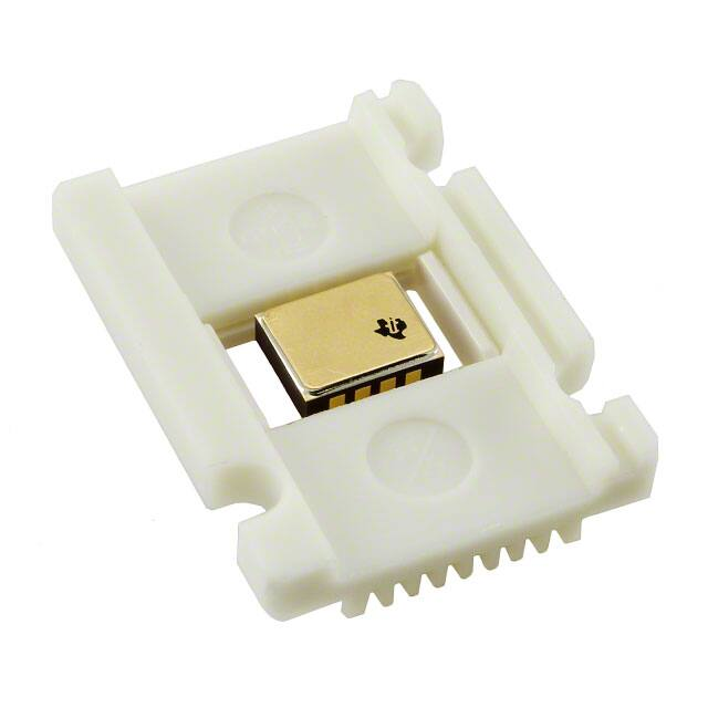
8-Pin Ceramic Package
Pin Compatible to ADS7816 and ADS7822
Serial ( SPI™/SSI) Interface
•
•
•
•
APPLICATIONS
•
•
•
•
•
•
•
•
•
•
(1)
Down-Hole Drilling
High Temperature Environments
Vibration/Modal Analysis
Multi-Channel Data Acquisition
Acoustics/Dynamic Strain Gauges
Pressure Sensors
Controlled Baseline
One Assembly/Test Site
One Fabrication Site
Available in Extreme (–55°C/210°C)
Temperature Range (1)
Extended Product Life Cycle
Extended Product-Change Notification
Product Traceability
Texas Instruments' high temperature products
utilize highly optimized silicon (die) solutions
with design and process enhancements to
maximize performance over extended
temperatures.
Custom temperature ranges available
DESCRIPTION
The ADS8320 is a 16-bit, sampling analog-to-digital (A/D) converter with ensured specifications over a 2.7-V to
5.25-V supply range. It requires very little power even when operating at the full 100-kHz data rate. At lower data
rates, the high speed of the device enables it to spend most of its time in the power-down mode—the average
power dissipation is less than 100 mW at 10-kHz data rate.
The ADS8320 also features operation from 2 V to 5.25 V, a synchronous serial (SPI/SSI compatible) interface,
and a differential input. The reference voltage can be set to any level within the range of 500 mV to VCC.
Ultra-low power and small size make the ADS8320 ideal for portable and battery-operated systems. It is also a
perfect fit for remote data acquisition modules, simultaneous multi-channel systems, and isolated data
acquisition. The ADS8320 is available in 8-pin ceramic surface-mount packages, specified for the –55°C to
210°C temperature range.
SAR
Control
VREF
DOUT
+IN
Serial
Interface
CDAC
DCLOCK
–IN
S/H Amp
Comparator
CS/SHDN
1
2
Please be aware that an important notice concerning availability, standard warranty, and use in critical applications of
Texas Instruments semiconductor products and disclaimers thereto appears at the end of this data sheet.
SPI is a trademark of Motorola, Inc..
PRODUCTION DATA information is current as of publication date.
Products conform to specifications per the terms of the Texas
Instruments standard warranty. Production processing does not
necessarily include testing of all parameters.
Copyright © 2010–2012, Texas Instruments Incorporated
�ADS8320-HT
SBAS521B – DECEMBER 2010 – REVISED SEPTEMBER 2012
www.ti.com
This integrated circuit can be damaged by ESD. Texas Instruments recommends that all integrated circuits be handled with
appropriate precautions. Failure to observe proper handling and installation procedures can cause damage.
ESD damage can range from subtle performance degradation to complete device failure. Precision integrated circuits may be more
susceptible to damage because very small parametric changes could cause the device not to meet its published specifications.
ORDERING INFORMATION (1)
TA
–55°C to 210°C
ORDERABLE PART
NUMBER
PACKAGE
PACKAGE QTY | CARRIER
1 | TUBE
HKJ
ADS8320SHKJ
ADS8320SHKJ
HKQ
ADS8320SHKQ
ADS8320SHKQ
1 | TUBE
ADS8320SKGD1
NA
240 | TRAY
ADS8320SKGD2
NA
10 | TRAY
KGD
(1)
TOP-SIDE MARKING
For the most current package and ordering information, see the Package Option Addendum at the end of this document, or see the TI
Web site at www.ti.com.
BARE DIE INFORMATION
DIE THICKNESS
BACKSIDE FINISH
BACKSIDE
POTENTIAL
BOND PAD
METALLIZATION COMPOSITION
15 mils
Silicon backgrind
GND
Al-Si-Cu
Origin
a
c
b
d
2
Submit Documentation Feedback
Copyright © 2010–2012, Texas Instruments Incorporated
Product Folder Links: ADS8320-HT
�ADS8320-HT
www.ti.com
SBAS521B – DECEMBER 2010 – REVISED SEPTEMBER 2012
Table 1. Bond Pad Coordinates in Microns - Rev A
DISCRIPTION
PAD NUMBER
a
b
c
d
VREF
1
157.3
1437.4
259.5
1669.6
+IN
2
157.3
1149.4
256.6
1248.7
-IN
3
157.3
432.3
256.6
531.6
GND
4
171.2
137.4
270.4
366.6
CS/SHDN
5
1183.1
141.3
1282.4
240.6
DOUT
6
1183.1
448.6
1282.4
547.8
DCLOCK
7
1183.1
1011.1
1282.4
1110.4
+VCC
8
1183.1
1462.8
1282.4
1692
VREF
+Vcc
+IN
DCLOCK
Dout
-IN
GND
CSn/SHDN
Submit Documentation Feedback
Copyright © 2010–2012, Texas Instruments Incorporated
Product Folder Links: ADS8320-HT
3
�ADS8320-HT
SBAS521B – DECEMBER 2010 – REVISED SEPTEMBER 2012
www.ti.com
ABSOLUTE MAXIMUM RATINGS
Over operating free-air temperature range (unless otherwise noted). (1)
UNIT
VCC
6
Analog input voltage
V
-0.3 to 6
V
100
°C
Junction temperature
–55 to 210
°C
Storage temperature
–55 to 210
°C
Case temperature
External referance voltage
5.5
V
Input current to any pin except supply
±10
mA
(1)
Stresses above these ratings may cause permanent damage. Exposure to absolute maximum conditions for extended periods may
degrade device reliability. These are stress ratings only, and functional operation of the device at these or any other conditions beyond
those specified is not implied.
THERMAL CHARACTERISTICS FOR HKJ OR HKQ PACKAGE
over operating free-air temperature range (unless otherwise noted)
PARAMETER
θJC
MIN
TYP
MAX
to ceramic side of case
Junction-to-case thermal resistance
5.7
to top of case lid (metal side of case)
13.7
UNIT
°C/W
ELECTRICAL CHARACTERISTICS
VCC = 2.7 V, VREF = 2.5 V, -IN = GND, fSAMPLE = 100 kHz and fCLK = 24 x fSAMPLE, unless otherwise noted.
CONDITIONS
PARAMETER
TA = 210°C (1)
TA = -55°C to 125°C
MIN
TYP
MAX
Resolution
MIN
TYP
16
UNIT
MAX
16
Bits
Analog Input
Full-zcale input span
+IN – (–IN)
Absolute input range
0
VREF
0
VREF
+IN
–0.1
VCC + 0.1
–0.1
VCC + 0.1
–IN
–0.1
0.5
–0.1
0.5
Capacitance
Leakage current
V
V
45
45
pF
1
1
nA
System Performance
No missing codes
14
Integral linearity error
14
±0.032
±0.018
±0.034
±3.8
±0.5
±3.8
Offset error
VIN = 3 V
±0.6
Offset temperature drift
VIN = 3 V
±3
Gain error
VIN = 3 V
Gain temperature drift
VIN = 3 V
(1)
(2)
4
2.7 V < VCC < 3.3 V
% of FSR
mV
μV/°C
±4
±0.05
Noise
Power-supply rejection ratio
Bits
±0.008
±0.05
% of FSR
±0.3
±0.3
ppm/°C
20
21
μVrms
3
5
LSB (2)
Minimum and maximum parameters are characterized for operation at TA = 210°C, but may not be production tested at that
temperature. Production test limits with statistical guardbands are used to ensure high temperature performance.
LSB means least significant bit. With VREF = 2.5 V, one LSB is 0.038 V.
Submit Documentation Feedback
Copyright © 2010–2012, Texas Instruments Incorporated
Product Folder Links: ADS8320-HT
�ADS8320-HT
www.ti.com
SBAS521B – DECEMBER 2010 – REVISED SEPTEMBER 2012
ELECTRICAL CHARACTERISTICS (continued)
VCC = 2.7 V, VREF = 2.5 V, -IN = GND, fSAMPLE = 100 kHz and fCLK = 24 x fSAMPLE, unless otherwise noted.
CONDITIONS
PARAMETER
TA = 210°C (1)
TA = -55°C to 125°C
MIN
TYP
MAX
MIN
TYP
UNIT
MAX
Sampling Dynamics
Conversion time
16
Acquisition time
4.5
16
4.5
Throughput rate
Clk cycles
100
Clock frequency range
0.02
2.4
Clk cycles
0.02
100
kHz
2.4
MHz
Dynamic Characteristics
Total harmonic distortion
VIN = 2.7 x Vp-p at 1 kHz
-86
-82
dB
SINAD
VIN = 2.7 x Vp-p at 1 kHz
84
79
dB
Spurious-free dynamic range
VIN = 2.7 x Vp-p at 1 kHz
86
82
dB
88
83
dB
SNR
Reference Input
Voltage range
0.5
Resistance
Current drain
VCC
0.5
VCC
CS = GND, fSAMPLE = 0 Hz
5
5
CS = VCC
5
5
20
50
25
55
CS = VCC
0.1
7
0.9
12
V
GΩ
µA
Digital Input/Output
Logic family
Logic Levels
CMOS
CMOS
VIH
IIH = 5 µA
2
VCC + 0.3
2
VCC + 0.3
V
VIL
IIL = 5 µA
-0.3
0.8
-0.3
0.8
V
VOH
IOH = –250 µA
2.1
VOL
IOL = 250 µA
2.1
V
0.4
Data format
0.4
V
V
Straight binary
Power Supply Requirements
VCC
Specified performance
VCC range (3)
Quiescent current
See
(4)
2.7
3.3
2.7
3.3
2
5.25
2
5.25
2
2.7
2
2.7
850
fSAMPLE = 10 kHz (5) (6)
Power dissipation
Power-down
1300
650
100
CS = VCC
1300
100
2.3
3.8
1.75
0.3
4
6
3.8
V
µA
mW
µA
Temperature Range
Specified performance
(3)
(4)
(5)
(6)
-55
125
-55
210
°C
See the Typical Performance Curves for more information.
The maximum clock rate of the ADS8320 is less than 2.4 MHz in this power supply range.
fCLK = 2.4 MHz, CS = VCC for 216 clock cycles out of every 240.
See the Power Dissipation section for more information regarding lower sample rates.
Submit Documentation Feedback
Copyright © 2010–2012, Texas Instruments Incorporated
Product Folder Links: ADS8320-HT
5
�ADS8320-HT
SBAS521B – DECEMBER 2010 – REVISED SEPTEMBER 2012
www.ti.com
ELECTRICAL CHARACTERISTICS
VCC = 5 V, VREF = 5 V, -IN = GND, fSAMPLE = 100 kHz and fCLK = 24 x fSAMPLE, unless otherwise noted.
CONDITIONS
PARAMETER
TA = 210°C (1)
TA = -55°C to 125°C
MIN
TYP
MAX
Resolution
MIN
TYP
16
UNIT
MAX
16
Bits
Analog Input
Full-zcale input span
+IN – (–IN)
Absolute input range
0
VREF
0
VREF
+IN
–0.1
VCC + 0.1
–0.1
VCC + 0.1
–IN
–0.1
0.5
–0.1
0.5
Capacitance
Leakage current
V
V
45
45
pF
1
1
nA
System Performance
No missing codes
14
Integral linearity error
Offset error
Offset temperature drift
14
Bits
±0.008
±0.032
±0.018
±0.034
±0.6
±3.8
±0.5
±3.8
±3
Gain error
Noise
Power-supply rejection ratio
4.7 V < VCC < 5.25 V
mV
μV/°C
±4
±0.05
Gain temperature drift
% of FSR
±0.05
% of FSR
±0.3
±0.3
ppm/°C
20
21
μVrms
3
35
LSB (2)
Sampling Dynamics
Conversion time
16
Acquisition time
4.5
16
4.5
Throughput rate
Clk cycles
100
Clock frequency range
0.02
2.4
Clk cycles
0.02
100
kHz
2.4
MHz
Dynamic Characteristics
Total harmonic distortion
VIN = 5 x Vp-p at 10 kHz
-84
-83
dB
SINAD
VIN = 5 x Vp-p at 10 kHz
82
81
dB
Spurious-free dynamic range
VIN = 5 x Vp-p at 10 kHz
84
83
dB
90
88
dB
SNR
Reference Input
Voltage range
0.5
Resistance
VCC
VCC
5
5
CS = VCC
5
5
40
Current drain
0.5
CS = GND, fSAMPLE = 0 Hz
fSAMPLE = 10 kHz
0.8
CS = VCC
0.1
80
50
GΩ
80
0.8
5
2
V
µA
5
Digital Input/Output
Logic family
Logic Levels
CMOS
IIH = 5 µA
3
VCC + 0.3
3
VCC + 0.3
V
VIL
IIL = 5 µA
-0.3
0.8
-0.3
0.8
V
VOH
IOH = –250 µA
VOL
IOL = 250 µA
4
Data format
(1)
(2)
6
CMOS
VIH
4
0.4
V
0.4
V
Straight binary
Minimum and maximum parameters are characterized for operation at TA = 210°C, but may not be production tested at that
temperature. Production test limits with statistical guardbands are used to ensure high temperature performance.
LSB means least significant bit. With VREF = 5 V, one LSB is 0.076 V.
Submit Documentation Feedback
Copyright © 2010–2012, Texas Instruments Incorporated
Product Folder Links: ADS8320-HT
�ADS8320-HT
www.ti.com
SBAS521B – DECEMBER 2010 – REVISED SEPTEMBER 2012
ELECTRICAL CHARACTERISTICS (continued)
VCC = 5 V, VREF = 5 V, -IN = GND, fSAMPLE = 100 kHz and fCLK = 24 x fSAMPLE, unless otherwise noted.
CONDITIONS
PARAMETER
TA = 210°C (1)
TA = -55°C to 125°C
MIN
TYP
UNIT
MAX
MIN
TYP
MAX
4.75
5.25
4.75
5.25
V
2
5.25
2
5.25
V
Power Supply Requirements
VCC
Specified performance
VCC range (3)
1150
Quiescent current
fSAMPLE = 10 kHz (4) (5)
850
200
Power dissipation
Power-down
1700
CS = VCC
1700
µA
200
5.5
8.5
4.5
0.3
3
5
8.5
mW
µA
Temperature Range
Specified performance
(3)
(4)
(5)
-55
125
-55
210
°C
See the Typical Performance Curves for more information.
fCLK = 2.4 MHz, CS = VCC for 216 clock cycles out of every 240.
See the Power Dissipation section for more information regarding lower sample rates.
PIN CONFIGURATION
HKJ PACKAGE
(TOP VIEW)
VREF 1
HKQ PACKAGE
(TOP VIEW)
8
+VCC
7
DCLOCK
+VCC
+IN
2
–IN
3
6
DOUT
GND 4
5
CS/SHDN
ADS8320
8
1
VREF
DCLOCK
+IN
DOUT
-IN
GND
CS/SHDN
5
4
HKQ as formed or HKJ mounted dead bug
PIN ASSIGNMENTS
PIN #
NAME
DESCRIPTION
1
VREF
Reference input
2
+IN
Noninverting input
3
-IN
Inverting input. Connect to ground or to remote ground sense point.
4
GND
5
CS/SHDN
6
DOUT
7
DCLOCK
8
+VCC
Ground
Chip select when LOW, shutdown mode when HIGH.
The serial output data word is comprised of 16 bits of data. In operation the data is valid on the falling edge of DCLOCK. The
second clock pulse after the falling edge of CS enables the serial output. After one null bit the data is valid for the next 16
edges.
Data clock synchronizes the serial data transfer and determines conversion speed.
Power supply
Submit Documentation Feedback
Copyright © 2010–2012, Texas Instruments Incorporated
Product Folder Links: ADS8320-HT
7
�ADS8320-HT
SBAS521B – DECEMBER 2010 – REVISED SEPTEMBER 2012
www.ti.com
xxx
TYPICAL CHARACTERISTICS
At TA = 25°C, VCC = 5 V, VREF = 5 V, fSAMPLE = 100 kHz, and fCLK = 24 x fSAMPLE, unless otherwise specified.
INTEGRAL LINEARITY ERROR
vs
CODE (25°C)
DIFFERENTIAL LINEARITY ERROR
vs
CODE (25°C)
3.0
1.0
Differential Linearity Error (LSB)
Integral Linearity Error (LSB)
20
0.0
–1.0
–2.0
–3.0
–4.0
–5.0
–6.0
0000H
4000H
8000H
C000H
2.0
1.0
0.0
–1.0
–2.0
–3.0
0000H
FFFFH
4000H
C000H
Figure 1.
Figure 2.
SUPPLY CURRENT
vs
TEMPERATURE
POWER-DOWN SUPPLY CURRENT
vs
TEMPERATURE
1400
FFFFH
6000
1200
5000
5V
1000
Supply Current (nA)
Supply Current (µA)
8000H
Hex Code
Hex Code
2.7V
800
600
400
4000
3000
2000
1000
5V
200
0
−55
0
0
55
110
Temperature (°C)
165
220
−1000
−55
Figure 3.
8
0
55
110
Temperature (°C)
165
220
Figure 4.
Submit Documentation Feedback
Copyright © 2010–2012, Texas Instruments Incorporated
Product Folder Links: ADS8320-HT
�ADS8320-HT
www.ti.com
SBAS521B – DECEMBER 2010 – REVISED SEPTEMBER 2012
TYPICAL CHARACTERISTICS (continued)
At TA = 25°C, VCC = 5 V, VREF = 5 V, fSAMPLE = 100 kHz, and fCLK = 24 x fSAMPLE, unless otherwise specified.
QUIESCENT CURRENT
vs
VCC
1000
1000
Sample Rate (kHz)
Quiescent Current (µA)
1200
800
600
100
10
400
1
200
1
2
3
4
1
5
2
3
4
VCC (V)
VCC (V)
Figure 5.
Figure 6.
CHANGE IN OFFSET
vs
REFERENCE VOLTAGE
CHANGE IN OFFSET
vs
TEMPERATURE
6
5
1
VCC = 5V
5
0
4
Delta from 25°C (LSB)
Change in Offset (LSB)
MAXIMUM SAMPLE RATE
vs
VCC
3
2
1
0
–1
–2
2.7V
−1
5V
−2
−3
−4
−5
–3
1
2
3
Reference Voltage (V)
4
−6
−55
5
55
110
Temperature (°C)
Figure 7.
Figure 8.
CHANGE IN GAIN
vs
REFERENCE VOLTAGE
CHANGE IN GAIN
vs
TEMPERATURE
165
220
165
220
1
5
VCC = 5V
4
0
3
−1
Delta from 25°C (LSB)
Change in Gain (LSB)
0
2
1
0
5V
−2
2.7V
−3
−4
−5
–1
−6
–2
1
2
3
Reference Voltage (V)
4
5
−7
−55
Figure 9.
0
55
110
Temperature (°C)
Figure 10.
Submit Documentation Feedback
Copyright © 2010–2012, Texas Instruments Incorporated
Product Folder Links: ADS8320-HT
9
�ADS8320-HT
SBAS521B – DECEMBER 2010 – REVISED SEPTEMBER 2012
www.ti.com
TYPICAL CHARACTERISTICS (continued)
At TA = 25°C, VCC = 5 V, VREF = 5 V, fSAMPLE = 100 kHz, and fCLK = 24 x fSAMPLE, unless otherwise specified.
PEAK-TO-PEAK NOISE
vs
REFERENCE VOLTAGE
FREQUENCY SPECTRUM
(8192 Point FFT, FIN = 10.120 kHz, –0.3 dB)
0
10
Peak-to-Peak Noise (LSB)
–40
Amplitude (dB)
VCC = 5V
9
–20
–60
–80
–100
–120
8
7
6
5
4
3
2
1
–140
0
0
10
30
20
40
50
0.1
Frequency (kHz)
Figure 11.
Figure 12.
SPURIOUS-FREE DYNAMIC RANGE AND SIGNAL-TONOISE RATIO
vs
FREQUENCY
TOTAL HARMONIC DISTORTION
vs
FREQUENCY
Signal-to-Noise Ratio
90
–10
Total Harmonic Distortion (dB)
Spurious-Free Dynamic Range
and Signal-to-Noise Ratio (dB)
10
0
100
80
Spurious-Free Dynamic Range
70
60
50
40
30
20
–20
–30
–40
–50
–60
–70
–80
10
–90
0
–100
1
10
50
100
1
Frequency (kHz)
Figure 13.
10
1
Reference Voltage (V)
10
Frequency (kHz)
100
Figure 14.
Submit Documentation Feedback
Copyright © 2010–2012, Texas Instruments Incorporated
Product Folder Links: ADS8320-HT
�ADS8320-HT
www.ti.com
SBAS521B – DECEMBER 2010 – REVISED SEPTEMBER 2012
TYPICAL CHARACTERISTICS (continued)
At TA = 25°C, VCC = 5 V, VREF = 5 V, fSAMPLE = 100 kHz, and fCLK = 24 x fSAMPLE, unless otherwise specified.
SIGNAL-TO-(NOISE + DISTORTION)
vs
FREQUENCY
SIGNAL-TO-(NOISE + DISTORTION)
vs
INPUT LEVEL
90
Signal-to-(Noise + Distortion) (dB)
Signal-to-(Noise + Distortion) (dB)
100
90
80
70
60
50
40
30
20
10
10
50
70
60
50
40
30
20
–40
0
1
80
100
–35
–30
Frequency (kHz)
–10
Figure 15.
Figure 16.
REFERENCE CURRENT
vs
SAMPLE RATE
REFERENCE CURRENT
vs
TEMPERATURE
–5
0
70
70
60
60
Reference Current (µA)
Reference Current (µA)
–25
–20
–15
Input Level (dB)
50
40
5V
30
20
2.7V
10
5V
50
40
30
2.7V
20
0
0
20
40
60
Sample Rate (kHz)
80
100
10
−55
Figure 17.
0
55
110
Temperature (°C)
165
220
Figure 18.
Submit Documentation Feedback
Copyright © 2010–2012, Texas Instruments Incorporated
Product Folder Links: ADS8320-HT
11
�ADS8320-HT
SBAS521B – DECEMBER 2010 – REVISED SEPTEMBER 2012
www.ti.com
THEORY OF OPERATION
The ADS8320 is a classic successive approximation register (SAR) analog-to-digital (A/D) converter. The
architecture is based on capacitive redistribution, which inherently includes a sample/hold function. The converter
is fabricated on a 0.6μ CMOS process. The architecture and process allow the ADS8320 to acquire and convert
an analog signal at up to 100,000 conversions per second while consuming less than 4.5 mW from+VCC.
The ADS8320 requires an external reference, an external clock, and a single power source (VCC). The external
reference can be any voltage between 500 mV and VCC. The value of the reference voltage directly sets the
range of the analog input. The reference input current depends on the conversion rate of the ADS8320.
The external clock can vary between 24 kHz (1-kHz throughput) and 2.4 MHz (100-kHz throughput). The duty
cycle of the clock is essentially unimportant, as long as the minimum high and low times are at least 200 ns
(VCC = 2.7 V or greater). The minimum clock frequency is set by the leakage on the capacitors internal to the
ADS8320.
The analog input is provided to two input pins: +IN and –IN. When a conversion is initiated, the differential input
on these pins is sampled on the internal capacitor array. While a conversion is in progress, both inputs are
disconnected from any internal function.
The digital result of the conversion is clocked out by the DCLOCK input and is provided serially, most significant
bit first, on the DOUT pin. The digital data that is provided on the DOUT pin is for the conversion currently in
progress—there is no pipeline delay. It is possible to continue to clock the ADS8320 after the conversion is
complete and to obtain the serial data least significant bit first. See the digital timing section for more information.
ANALOG INPUT
The +IN and –IN input pins allow for a differential input signal. Unlike some converters of this type, the –IN input
is not re-sampled later in the conversion cycle. When the converter goes into the hold mode, the voltage
difference between +IN and –IN is captured on the internal capacitor array.
The range of the –IN input is limited to –0.1 V to 1 V (–0.1 V to 0.5 V when using a 2.7-V supply). Because of
this, the differential input can be used to reject only small signals that are common to both inputs. Thus, the –IN
input is best used to sense a remote signal ground that may move slightly with respect to the local ground
potential.
The input current on the analog inputs depends on a number of factors: sample rate, input voltage, source
impedance, and power-down mode. Essentially, the current into the ADS8320 charges the internal capacitor
array during the sample period. After this capacitance has been fully charged, there is no further input current.
The source of the analog input voltage must be able to charge the input capacitance (45 pF) to a 16-bit settling
level within 4.5 clock cycles. When the converter goes into the hold mode or while it is in the powerdown mode,
the input impedance is greater than 1 GΩ.
Care must be taken regarding the absolute analog input voltage. To maintain the linearity of the converter, the
–IN input should not drop below GND – 100 mV or exceed GND + 1 V. The +IN input should always remain
within the range of GND – 100 mV to VCC + 100 mV. Outside of these ranges, the converter linearity may not
meet specifications. To minimize noise, low bandwidth input signals with lowpass filters should be used.
REFERENCE INPUT
The external reference sets the analog input range. The ADS8320 operates with a reference in the range of
500 mV to VCC. There are several important implications of this.
As the reference voltage is reduced, the analog voltage weight of each digital output code is reduced. This is
often referred to as the Least Significant Bit (LSB) size and is equal to the reference voltage divided by 65,536.
This means that any offset or gain error inherent in the A/D converter will appear to increase, in terms of LSB
size, as the reference voltage is reduced.
The noise inherent in the converter also appears to increase with lower LSB size. With a 5-V reference, the
internal noise of the converter typically contributes only 1.5 LSB peak-to-peak of potential error to the output
code. When the external reference is 500 mV, the potential error contribution from the internal noise will be 10
times larger—15 LSBs. The errors due to the internal noise are gaussian in nature and can be reduced by
averaging consecutive conversion results.
12
Submit Documentation Feedback
Copyright © 2010–2012, Texas Instruments Incorporated
Product Folder Links: ADS8320-HT
�ADS8320-HT
www.ti.com
SBAS521B – DECEMBER 2010 – REVISED SEPTEMBER 2012
For more information regarding noise, consult the typical performance curve “Peak-to-Peak Noise vs Reference
Voltage.” Note that the Effective Number of Bits (ENOB) figure is calculated based on the converter’s signal-to(noise + distortion) ratio with a 1-kHz, 0-dB input signal. SINAD is related to ENOB as follows:
SINAD = 6.02 · ENOB + 1.76
(1)
With lower reference voltages, extra care should be taken to provide a clean layout including adequate
bypassing, a clean power supply, a low-noise reference, and a low-noise input signal. Because the LSB size is
lower, the converter is also more sensitive to external sources of error such as nearby digital signals and
electromagnetic interference.
NOISE
The noise floor of the ADS8320 itself is extremely low, as can be seen in Figure 19 and Figure 20, and is much
lower than competing A/D converters. It was tested by applying a lownoise DC input and a 5-V reference to the
ADS8320 and initiating 5000 conversions. The digital output of the A/D converter varies in output code due to the
internal noise of the ADS8320. This is true for all 16-bit SAR-type A/D converters. Using a histogram to plot the
output codes, the distribution should appear bell-shaped with the peak of the bell curve representing the nominal
code for the input value. The ±1σ, ±2σ and ±3σ distributions represents the 68.3%, 95.5%, and 99.7%,
respectively, of all codes. The transition noise can be calculated by dividing the number of codes measured by 6
and this yields the ±3σ distribution or 99.7% of all codes. Statistically, up to 3 codes could fall outside the
distribution when executing 1000 conversions. The ADS8320, with < 3 output codes for ±3σ distribution, yields a
< ±0.5 LSB transition noise. Remember, to achieve this low noise performance, the peak-to-peak noise of the
input signal and reference must be < 50 µV.
2510
0
0
1
2
2490
3
4
0
0
5
6
Code
Figure 19. Histogram of 5000 Conversions of a DC Input at the Code Transition
Submit Documentation Feedback
Copyright © 2010–2012, Texas Instruments Incorporated
Product Folder Links: ADS8320-HT
13
�ADS8320-HT
SBAS521B – DECEMBER 2010 – REVISED SEPTEMBER 2012
www.ti.com
4864
0
0
72
1
2
3
4
64
0
5
6
Code
Figure 20. Histogram of 5000 Conversions of a DC Input at the Code Center
14
Submit Documentation Feedback
Copyright © 2010–2012, Texas Instruments Incorporated
Product Folder Links: ADS8320-HT
�ADS8320-HT
www.ti.com
SBAS521B – DECEMBER 2010 – REVISED SEPTEMBER 2012
DIGITAL INTERFACE
SIGNAL LEVELS
The digital inputs of the ADS8320 can accommodate logic levels up to 5.5 V regardless of the value of VCC.
Thus, the ADS8320 can be powered at 3 V and still accept inputs from logic powered at 5 V.
The CMOS digital output (DOUT) swings 0 V to VCC. If VCC is 3 V and this output is connected to a 5-V CMOS
logic input, then that IC may require more supply current than normal and may have a slightly longer propagation
delay.
SERIAL INTERFACE
The ADS8320 communicates with microprocessors and other digital systems via a synchronous 3-wire serial
interface, as shown in Figure 21 and Table 2. The DCLOCK signal synchronizes the data transfer with each bit
being transmitted on the falling edge of DCLOCK. Most receiving systems will capture the bitstream on the rising
edge of DCLOCK. However, if the minimum hold time for DOUT is acceptable, the system can use the falling edge
of DCLOCK to capture each bit.
A falling CS signal initiates the conversion and data transfer. The first 4.5 to 5.0 clock periods of the conversion
cycle are used to sample the input signal. After the fifth falling DCLOCK edge, DOUT is enabled and outputs a
LOW value for one clock period. For the next 16 DCLOCK periods, DOUT outputs the conversion result, most
significant bit first. After the least significant bit (B0) has been output, subsequent clocks repeat the output data
but in a least significant bit first format.
After the most significant bit (B15) has been repeated, DOUT will tri-state. Subsequent clocks will have no effect
on the converter. A new conversion is initiated only when CS has been taken HIGH and returned LOW.
Table 2. Timing Specifications (VCC = 2.7 V and Above, –55°C to 210°C)
SYMBOL
DESCRIPTION
MIN
TYP
MAX
4.5
UNIT
tSMPL
Analog input sample time
tCONV
Conversion time
5
tCYC
Throughput rate
tCSD
CS falling to DCLOCK LOW
tSUCS
CS falling to DCLOCK Rising
thDO
DCLOCK falling to current DOUT not valid
tdDO
DCLOCK falling to next DOUT valid
30
50
ns
tdis
CS rising to DOUT tri-state
70
100
ns
ten
DCLOCK falling to DOUT enabled
20
50
ns
tf
DOUT fall time
5
25
ns
tr
DOUT rise time
7
25
ns
16
Clk cycles
Clk cycles
100
kHz
0
ns
20
ns
5
15
ns
DATA FORMAT
The output data from the ADS8320 is in straight binary format, as shown in Table 3. This table represents the
ideal output code for the given input voltage and does not include the effects of offset, gain error, or noise.
Table 3. Ideal Input Voltages and Output Codes
DESCRIPTION
ANALOG VALUE
DIGITAL OUTPUT
STRAIGHT BINARY
BINARY CODE
HEX CODE
FFFF
Full-scale range
VREF
Least significant bit (LSB)
VREF/65,536
Full scale
VREF – 1 LSB
1111 1111 1111 1111
Midscale
VREF/2
1000 0000 0000 0000
8000
Midscale – 1 LSB
VREF/2 – 1 LSB
0111 1111 1111 1111
7FFF
Zero
0V
0000 0000 0000 0000
0000
Submit Documentation Feedback
Copyright © 2010–2012, Texas Instruments Incorporated
Product Folder Links: ADS8320-HT
15
�ADS8320-HT
SBAS521B – DECEMBER 2010 – REVISED SEPTEMBER 2012
www.ti.com
POWER DISSIPATION
The architecture of the converter, the semiconductor fabrication process, and a careful design allow the
ADS8320 to convert at up to a 100-kHz rate while requiring very little power. Still, for the absolute lowest power
dissipation, there are several things to keep in mind.
The power dissipation of the ADS8320 scales directly with conversion rate. Therefore, the first step to achieving
the lowest power dissipation is to find the lowest conversion rate that satisfies the requirements of the system.
In addition, the ADS8320 is in power-down mode under two conditions: when the conversion is complete and
whenever CS is HIGH (as shown in Figure 21). Ideally, each conversion should occur as quickly as possible,
preferably at a 2.4-MHz clock rate. This way, the converter spends the longest possible time in the power-down
mode. This is very important as the converter not only uses power on each DCLOCK transition (as is typical for
digital CMOS components), but also uses some current for the analog circuitry, such as the comparator. The
analog section dissipates power continuously, until the power-down mode is entered.
Complete Cycle
CS/SHDN
tSUCS
Sample
Power Down
Conversion
DCLOCK
tCSD
DOUT
Use positive clock edge for data transfer
Hi-Z
0
tSMPL
B15 B14 B13 B12 B11 B10 B9 B8 B7
(MSB)
tCONV
B6
B5 B4
B3
B2
B1 B0
(LSB)
Hi-Z
NOTE: Minimum 22 clock cycles required for 16-bit conversion. Shown are 24 clock cycles.
If CS remains LOW at the end of conversion, a new datastream with LSB-first is shifted out again.
Figure 21. ADS8320 Basic Timing Diagrams
16
Submit Documentation Feedback
Copyright © 2010–2012, Texas Instruments Incorporated
Product Folder Links: ADS8320-HT
�ADS8320-HT
www.ti.com
SBAS521B – DECEMBER 2010 – REVISED SEPTEMBER 2012
1.4V
3kΩ
DOUT
VOH
DOUT
VOL
Test Point
tr
100pF
CLOAD
tf
Voltage Waveforms for D OUT Rise and Fall Times, t r, tf
Load Circuit for tdDO, tr, and tf
Test Point
DCLOCK
VIL
VCC
DOUT
tdDO
VOH
DOUT
tdis Waveform 2, t en
3kΩ
tdis Waveform 1
100pF
CLOAD
VOL
thDO
Load Circuit for tdis and ten
Voltage Waveforms for D OUT Delay Times, t dDO
VIH
CS/SHDN
DOUT
Waveform 1 (1)
CS/SHDN
90%
DCLOCK
1
4
5
tdis
DOUT
Waveform 2 (2)
10%
VOL
DOUT
B11
ten
Voltage Waveforms for t dis
Voltage Waveforms for t en
NOTES: (1) Waveform 1 is for an output with internal conditions such that the output
is HIGH unless disabled by the output control. (2) Waveform 2 is for an output with
internal conditions such that the output is LOW unless disabled by the output control.
Figure 22. Timing Diagrams and Test Circuits for the Parameters in Table 2
Figure 23 shows the current consumption of the ADS8320 versus sample rate. For this graph, the converter is
clocked at 2.4 MHz regardless of the sample rate—CS is HIGH for the remaining sample period. Figure 24 also
shows current consumption versus sample rate. However, in this case, the DCLOCK period is 1/24th of the
sample period—CS is HIGH for one DCLOCK cycle out of every 16.
Submit Documentation Feedback
Copyright © 2010–2012, Texas Instruments Incorporated
Product Folder Links: ADS8320-HT
17
�ADS8320-HT
SBAS521B – DECEMBER 2010 – REVISED SEPTEMBER 2012
www.ti.com
1000
Supply Current (µA)
TA = 25°C
fCLK = 2.4MHz
100
VCC = 5.0V
VREF = 5.0V
VCC = 2.7V
VREF = 2.5V
10
1
0.1
1
10
100
Sample Rate (kHz)
Figure 23. Maintaining fCLK at the Highest Possible Rate Allows Supply Current to Drop Linearly With
Sample Rate
Supply Current (µA)
1000
100
10
TA = 25°C
VCC = 5.0V
VREF = 5.0V
fCLK = 24 • fSAMPLE
1
0.1
10
1
Sample Rate (kHz)
100
Figure 24. Scaling fCLK Reduces Supply Current Only Slightly With Sample Rate
There is an important distinction between the power-down mode that is entered after a conversion is complete
and the full power-down mode which is enabled when CS is HIGH. CS LOW will shut down only the analog
section. The digital section is completely shut down only when CS is HIGH. Thus, if CS is left LOW at the end of
a conversion and the converter is continually clocked, the power consumption will not be as low as when CS is
HIGH. Figure 25 shows more information.
1000
TA = 25°C
VCC = 5.0V
VREF = 5.0V
fCLK = 24 • fSAMPLE
Supply Current (mA)
800
600
CS LOW (GND)
400
200
0.0
CS HIGH (VCC)
0.250
0.00
0.1
1
10
100
Sample Rate (kHz)
Figure 25. Shutdown Current With CS HIGH is 50 nA Typically, Regardless of the Clock. Shutdown
Current With CS LOW Varies With Sample Rate
18
Submit Documentation Feedback
Copyright © 2010–2012, Texas Instruments Incorporated
Product Folder Links: ADS8320-HT
�ADS8320-HT
www.ti.com
SBAS521B – DECEMBER 2010 – REVISED SEPTEMBER 2012
Power dissipation can also be reduced by lowering the power-supply voltage and the reference voltage. The
ADS8320 operates over a VCC range of 2.0 V to 5.25 V. However, at voltages below 2.7 V, the converter will not
run at a 100-kHz sample rate. See the typical performance curves for more information regarding power supply
voltage and maximum sample rate.
SHORT CYCLING
Another way of saving power is to utilize the CS signal to short cycle the conversion. Because the ADS8320
places the latest data bit on the DOUT line as it is generated, the converter can easily be short cycled. This term
means that the conversion can be terminated at any time. For example, if only 14 bits of the conversion result
are needed, then the conversion can be terminated (by pulling CS HIGH) after the 14th bit has been clocked out.
This technique can be used to lower the power dissipation (or to increase the conversion rate) in those
applications where an analog signal is being monitored until some condition becomes true. For example, if the
signal is outside a predetermined range, the full 16-bit conversion result may not be needed. If so, the conversion
can be terminated after the first n bits, where n might be as low as 3 or 4. This results in lower power dissipation
in both the converter and the rest of the system, as they spend more time in the power-down mode.
Submit Documentation Feedback
Copyright © 2010–2012, Texas Instruments Incorporated
Product Folder Links: ADS8320-HT
19
�ADS8320-HT
SBAS521B – DECEMBER 2010 – REVISED SEPTEMBER 2012
www.ti.com
LAYOUT
(1)
For optimum performance, care should be taken with the physical layout of the ADS8320 circuitry. This is
particularly true if the reference voltage is low and/or the conversion rate is high. At a 100-kHz conversion rate,
the ADS8320 makes a bit decision every 416 ns. That is, for each subsequent bit decision, the digital output
must be updated with the results of the last bit decision, the capacitor array appropriately switched and charged,
and the input to the comparator settled to a 16-bit level all within one clock cycle.
The basic SAR architecture is sensitive to spikes on the power supply, reference, and ground connections that
occur just prior to latching the comparator output. Thus, during any single conversion for an n-bit SAR converter,
there are n “windows” in which large external transient voltages can easily affect the conversion result. Such
spikes might originate from switching power supplies, digital logic, and high power devices, to name a few. This
particular source of error can be very difficult to track down if the glitch is almost synchronous to the converter
DCLOCK signal—as the phase difference between the two changes with time and temperature, causing sporadic
misoperation.
With this in mind, power to the ADS8320 should be clean and well bypassed. A 0.1-μF ceramic bypass capacitor
should be placed as close to the ADS8320 package as possible. In addition, a 1-μF to 10-μF capacitor and a 5-Ω
or 10-Ω series resistor may be used to low-pass filter a noisy supply.
The reference should be similarly bypassed with a 0.1-μF capacitor. Again, a series resistor and large capacitor
can be used to low-pass filter the reference voltage. If the reference voltage originates from an op amp, be
careful that the op amp can drive the bypass capacitor without oscillation (the series resistor can help in this
case). Keep in mind that while the ADS8320 draws very little current from the reference on average, there are
still instantaneous current demands placed on the external input and reference circuitry.
Texas Instruments' OPA627 op amp provides optimum performance for buffering both the signal and reference
inputs. For low-cost, low-voltage, single-supply applications, the OPA2350 or OPA2340 dual op amps are
recommended.
Also, keep in mind that the ADS8320 offers no inherent rejection of noise or voltage variation in regards to the
reference input. This is of particular concern when the reference input is tied to the power supply. Any noise and
ripple from the supply will appear directly in the digital results. While high-frequency noise can be filtered out as
described in the previous paragraph, voltage variation due to the line frequency (50 Hz or 60 Hz), can be difficult
to remove.
The GND pin on the ADS8320 should be placed on a clean ground point. In many cases, this will be the “analog”
ground. Avoid connecting the GND pin too close to the grounding point for a microprocessor, microcontroller, or
digital signal processor. If needed, run a ground trace directly from the converter to the power-supply connection
point. The ideal layout includes an analog ground plane for the converter and associated analog circuitry.
(1)
20
OPA627, OPA2350 and OPA2340 have not been characterized or tested at 210°C.
Submit Documentation Feedback
Copyright © 2010–2012, Texas Instruments Incorporated
Product Folder Links: ADS8320-HT
�ADS8320-HT
www.ti.com
SBAS521B – DECEMBER 2010 – REVISED SEPTEMBER 2012
APPLICATION CIRCUITS
Figure 26 shows a basic data acquisition system. The ADS8320 input range is 0 V to VCC, as the reference input
is connected directly to the power supply. The 5-Ω resistor and 1-μF to 10-μF capacitor filter the microcontroller
“noise” on the supply, as well as any high-frequency noise from the supply itself. The exact values should be
picked such that the filter provides adequate rejection of the noise.
2.7V to 5.25V
5Ω
+ 1µF to
10µF
ADS8320
VREF
VCC
+IN
CS
–IN
DOUT
0.1µF
GND
+ 1µF to
10µF
Microcontroller
DCLOCK
Figure 26. Basic Data Acquisition System
Submit Documentation Feedback
Copyright © 2010–2012, Texas Instruments Incorporated
Product Folder Links: ADS8320-HT
21
�PACKAGE OPTION ADDENDUM
www.ti.com
4-Feb-2021
PACKAGING INFORMATION
Orderable Device
Status
(1)
Package Type Package Pins Package
Drawing
Qty
Eco Plan
(2)
Lead finish/
Ball material
MSL Peak Temp
Op Temp (°C)
Device Marking
(3)
(4/5)
(6)
ADS8320SHKJ
ACTIVE
CFP
HKJ
8
1
RoHS & Green
Call TI
N / A for Pkg Type
-55 to 210
ADS8320S
HKJ
ADS8320SHKQ
ACTIVE
CFP
HKQ
8
1
RoHS & Green
AU
N / A for Pkg Type
-55 to 210
ADS8320S
HKQ
ADS8320SKGD1
ACTIVE
XCEPT
KGD
0
240
RoHS & Green
Call TI
N / A for Pkg Type
-55 to 210
ADS8320SKGD2
ACTIVE
XCEPT
KGD
0
10
RoHS & Green
Call TI
N / A for Pkg Type
-55 to 210
(1)
The marketing status values are defined as follows:
ACTIVE: Product device recommended for new designs.
LIFEBUY: TI has announced that the device will be discontinued, and a lifetime-buy period is in effect.
NRND: Not recommended for new designs. Device is in production to support existing customers, but TI does not recommend using this part in a new design.
PREVIEW: Device has been announced but is not in production. Samples may or may not be available.
OBSOLETE: TI has discontinued the production of the device.
(2)
RoHS: TI defines "RoHS" to mean semiconductor products that are compliant with the current EU RoHS requirements for all 10 RoHS substances, including the requirement that RoHS substance
do not exceed 0.1% by weight in homogeneous materials. Where designed to be soldered at high temperatures, "RoHS" products are suitable for use in specified lead-free processes. TI may
reference these types of products as "Pb-Free".
RoHS Exempt: TI defines "RoHS Exempt" to mean products that contain lead but are compliant with EU RoHS pursuant to a specific EU RoHS exemption.
Green: TI defines "Green" to mean the content of Chlorine (Cl) and Bromine (Br) based flame retardants meet JS709B low halogen requirements of