��
%&�
SBAS277 – MAY 2003
�������
��
�
� ���������� �������� ������
����������� � ���!���"#$�#$
FEATURES
D True Bipolar Input
D Input Signal Range: ±2.5V
D 4-Channel Input Multiplexer
D Up to 250kSPS Sampling Rate
D Selectable 8-Bit or 16-Bit Parallel Interface
D 16-Bit Ensured No Missing Codes
D Offset: 1mV max
D Low Power: 200mW
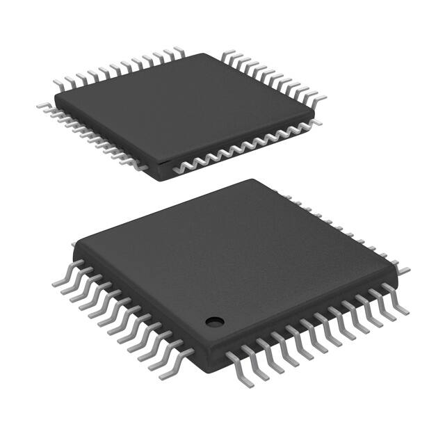
D TQFP-48 Package
D Operating Temperature Range: –40°C to +85°C
DESCRIPTION
The ADS8342 is a 4-channel, 16-bit analog-to-digital
converter (ADC). It contains a 16-bit succesive
approximation register (SAR), a capacitor-based ADC with
an inherent sample-and-hold circuit, an interface for
microprocessor use, and parallel 3-state output drivers. The
ADS8342 is specified at a 250kHz sampling rate while
dissipating only 200mW of power using a ±5V power supply.
The ADS8342 is available in a TQFP-48 package and is
ensured over the –40°C to +85°C temperature range.
APPLICATIONS
D Data Acquisition
D Test and Measurement
D Industrial Process Control
D Medical Instruments
D Laboratory Equipment
Please be aware that an important notice concerning availability, standard warranty, and use in critical applications of Texas Instruments
semiconductor products and disclaimers thereto appears at the end of this data sheet.
Copyright 2003, Texas Instruments Incorporated
�$��'�� �� ���� ��()�*���)� �+ ,������ �+ )( ��-��,���)� .���/ ��).�,�+
,)�()�* �) +��,�(�,���)�+ ��� ��� ���*+ )( ��0�+ �+���*���+ +���.��. 1������2/
��).�,��)� ��),�++��3 .)�+ �)� ��,�++����2 ��,��.� ��+���3 )( ��� ����*����+/
www.ti.com
���
%&�
www.ti.com
SBAS277 – MAY 2003
This integrated circuit can be damaged by ESD. Texas Instruments recommends that all integrated
circuits be handled with appropriate precautions. Failure to observe proper handling and installation
procedures can cause damage.
ESD damage can range from subtle performance degradation to complete device failure. Precision integrated circuits
may be more susceptible to damage because very small parametric changes could cause the device not to meet
its published specifications.
ORDERING INFORMATION
PRODUCT
MAXIMUM
INTEGRAL
LINEARITY
ERROR
(LSB)
ADS8342
ADS8342
NO
MISSING
CODES
(Bits)
±6
±4
PACKAGE–
LEAD
15
16
PACKAGE
DESIGNATOR(1)
TQFP 48
TQFP-48
TQFP 48
TQFP-48
PFB
PFB
SPECIFIED
TEMPERATURE
RANGE
ORDERING
NUMBER
TRANSPORT
MEDIA,
QUANTITY
ADS8342IPFBT
Tape and Reel,
250
ADS8342IPFBR
Tape and Reel,
2000
ADS8342IBPFBT
Tape and Reel,
250
ADS8342IBPFBR
Tape and Reel,
2000
–40°C
40°C to
t +85°C
85°C
–40°C
40°C tto +85°C
85°C
(1) For the most current specification and package information, refer to our web site at www.ti.com.
ABSOLUTE MAXIMUM RATINGS
over operating free-air temperature range unless otherwise noted(1)
ADS8342I
UNIT
Supply voltage, +AVDD to AGND and +DVDD to DGND
–0.3 to 6
V
Supply voltage, –AVDD to AGND and –DVDD to DGND
–6 to 0.3
V
Supply voltage, BVDD to BGND
Analog input voltage to AGND
Reference voltage, REFIN to AGND
Common voltage to AGND
Digital input voltage to BGND
Ground voltage differences, AGND to REFGND or BGND or DGND
Voltage differences, BVDD or +DVDD to AGND
Voltage differences, +DVDD to +AVDD and –DVDD to –AVDD
Voltage differences, BVDD to DVDD
Input current to any pin except supply
Power dissipation
–0.3 to 6
V
–AVDD – 0.3 to +AVDD + 0.3
–0.3 to +AVDD + 0.3
V
V
–0.3 to +0.3
V
BGND – 0.3 to BVDD + 0.3
V
–0.3 to 0.3
V
–0.3 to 6
V
–0.3 to 0.3
V
–(+DVDD) to 0.3
–20 to 20
mA
V
see Package Dissipation Ratings table
Operating virtual junction temperature range, TJ
–40 to +150
°C
Operating free-air temperature range, TA
–40 to +85
°C
Storage temperature range, TSTG
–65 to +150
°C
Lead temperature 1.6mm (1/16 inch) from case for 10 seconds
+300
°C
(1) Stresses above these ratings may cause permanent damage. Exposure to absolute maximum conditions for extended periods may degrade
device reliability. These are stress ratings only, and functional operation of the device at these or any other conditions beyond those specified is
not implied.
2
���
%&�
www.ti.com
SBAS277 – MAY 2003
PACKAGE DISSIPATION RATINGS
BOARD
PACKAGE
RΘJC
(°C/W)
RΘJA
(°C/W)
DERATING FACTOR
ABOVE TA ≤ +25°C
(mW/°C)
TA ≤ +25°C
POWER RATING
(mW)
TA ≤ +70°C
POWER RATING
(mW)
TA = +85°C
POWER RATING
(mW)
Low K
PFB
19.6
97.5
10.256
1282
820
666
High K
PFB
19.6
63.7
15.698
1962
1255
1020
(1) The JEDEC Low K(1s) board design used to derive this data was a 3 inch x 3 inch, 2-layer board with 2-ounce copper traces on top of the board.
(2) The JEDEC High K(2s2p) board design used to derive this data was a 3 inch x 3 inch, multilayer board with 1-ounce internal power and ground
planes and 2-ounce copper traces on the top and bottom of the board.
RECOMMENDED OPERATING CONDITIONS
MIN
NOM
MAX
UNIT
Supply voltage, +AVDD to AGND
4.75
5
5.25
V
Supply voltage, –AVDD to AGND
–5.25
–5
–4.75
V
Supply voltage,
voltage BVDD to BGND
Low-voltage levels
2.7
3.6
V
5V logic levels
4.5
V
Supply voltage, +DVDD to DGND
4.75
5
+DVDD
5.25
Supply voltage, –DVDD to DGND
–5.25
–5
–4.75
V
2.0
2.5
2.55
V
Reference input voltage
Analog input voltage
+REFIN
V
–0.3
0
+0.3
V
Ground differences, AGND to REFGND or BGND or DGND
–0.01
0
0.01
V
Voltage differences, +DVDD to +AVDD and –DVDD to –AVDD
–0.01
0
0.01
V
Common voltage
–REFIN
V
EQUIVALENT INPUT CIRCUIT
3
���
%&�
www.ti.com
SBAS277 – MAY 2003
ELECTRICAL CHARACTERISTICS
Over recommended operating free-air temperature range at –40°C to +85°C, ±AVDD = ±DVDD = ±5V, BVDD = +5V, VREF = +2.5V, fCLK = 5MHz, and
fSAMPLE = 250kSPS, unless otherwise noted.
ADS8342I
ADS8342IB
PARAMETER
TEST CONDITIONS
UNIT
MIN
TYP(1)
MAX
MIN TYP(1) MAX
Analog Input
Full-scale range (FSR)
AIN to Common
Input MUX on-resistance
Common = AGND
–VREF
500
+VREF
:
Ω
Input capacitance
Common = AGND
20
:
pF
Input leakage current
Common = AGND
±0.3
:
µA
Full power bandwidth
FS sinewave, –3dB
16
:
MHz
:
:
V
Voltage Accuracy
Resolution
16
:
Bits
No missing code
(NMC)
15
16
Bits
Integral linearity error (INL)
–6
±3
+6
–4
±2
+4
LSB
–2
±1
+2
–1
±0.6
+1.5
LSB
+2
–1
+1
mV
Differential nonlinearity (DNL)
Bipolar zero (offset) error (VOS)
AIN = Common = 0V
–2
Bipolar zero (offset) error drift (TCVOS)
AIN = Common = 0V
1
Bipolar zero (offset) error match
AIN = Common = 0V
0.150
Positive gain error (PGERR)
AIN = VREF, Common = 0V
Positive gain error drift (TCPGERR)
AIN = VREF, Common = 0V
1.5
Positive gain error match
AIN = VREF, Common = 0V
0.003
Negative gain error (NGERR)
AIN = –VREF, Common = 0V
Negative gain error drift (TCNGERR)
AIN = –VREF, Common = 0V
1.5
Negative gain error match
AIN = –VREF, Common = 0V
0.003
–0.25
+0.25
–0.25
ppm/°C
:
1
:
:
:
mV
:
% FSR
ppm/°C
:
0.01
+0.25
:
:
:
:
% FSR
ppm/°C
:
0.01
% FSR
:
% FSR
:
:
µs
:
:
µs
:
Sampling Dynamics
Conversion time (tCONV)
500kHz ≤ fCLK ≤ 5MHz
3.4
Acquisition time (tACQ)
fCLK = 5MHz
0.6
34
Throughput rate
250
Multiplexer settling time
150
:
kHz
:
ns
Aperture delay
8
:
ns
Aperture jitter
50
:
ps
–89
:
dB
92
:
dB
86
:
dB
84.6
:
dB
AC Accuracy
Total haromonic distortion (THD)
Spurious-free dynamic range (SFDR)
Signal-to-noise ratio (SNR)
Signal-to-noise + distortion (SINAD)
Channel-to-channel isolation(2)
VIN = ±2.5Vp–p at 10kHz
VIN = ±2.5Vp–p at 10kHz
VIN = ±2.5Vp–p at 10kHz
VIN = ±2.5Vp–p at 10kHz
VIN = ±2.5Vp–p at 50kHz
95
Effective number of bits (ENOB)
Indicates the same specifications as the ADS8342I.
(1) All typical values are at TA = +25°C.
(2) Ensured by design.
(3) Applies for 5.0V nominal supply: BVDD (min) = 4.5V and BVDD (max) = 5.5V.
(4) Applies for 3.0V nominal supply: BVDD (min) = 2.7V and BVDD (max) = 3.6V.
:
4
dB
:
14
:
Bits
���
%&�
www.ti.com
SBAS277 – MAY 2003
ELECTRICAL CHARACTERISTICS (continued)
Over recommended operating free-air temperature range at –40°C to +85°C, ±AVDD = ±DVDD = ±5V, BVDD = +5V, VREF = +2.5V, fCLK = 5MHz, and
fSAMPLE = 250kSPS, unless otherwise noted.
ADS8342I
ADS8342IB
PARAMETER
TEST CONDITIONS
UNIT
MIN
TYP(1)
MAX
MIN TYP(1) MAX
Voltage Reference Input
Reference voltage
2.0
Reference input resistance
2.5
2.55
:
:
:
V
100
:
MΩ
Reference input capacitance
5
:
pF
Reference input current
5V Digital Inputs(3)
25
:
nA
Logic family
CMOS
High-level input voltage (VIH)
0.7 × BVDD
BVDD + 0.3
V
Low-level input voltage (VIL)
–0.3
0.3 × BVDD
V
Input leakage current (IIN)
VI = BVDD or GND
Input capacitance (CI)
5V Digital Outputs(3)
Logic family
High-level output voltage (VOH)
±50
nA
5
pF
CMOS
Low-level output voltage (VOL)
IOH = –100µA
IOL = +100µA
High-impeadance-state output current
(IOZ)
CS = BVDD, VO = BVDD or
GND
4.4
V
0.5
Output capacitance (CO)
±50
nA
5
pF
Load capacitance (CL)
20
Data format
V
pF
Binary Two’s Complement
3V Digital Inputs(4)
Logic family
High-level input voltage (VIH)
LVCMOS
Low-level input voltage (VIL)
BVDD = 3.6V
BVDD = 2.7V
Input leakage current (IIN)
VI = BVDD or GND
2
BVDD + 0.3
V
–0.3
0.8
V
Input capacitance (CI)
3V Digital Outputs(4)
Logic family
High-level output voltage (VOH)
nA
5
pF
LVCMOS
Low-level output voltage (VOL)
BVDD = 2.7V, IOH = –100µA
BVDD = 2.7V, IOL = +100µA
High-impeadance-state output current
(IOZ)
CS = BVDD, VO = BVDD or
GND
V
BVDD – 0.3
0.2
Output capacitance (CO)
Load capacitance (CL)
Data format
±50
V
±50
nA
5
pF
20
pF
Binary Two’s Complement
Indicates the same specifications as the ADS8342I.
(1) All typical values are at TA = +25°C.
(2) Ensured by design.
(3) Applies for 5.0V nominal supply: BVDD (min) = 4.5V and BVDD (max) = 5.5V.
(4) Applies for 3.0V nominal supply: BVDD (min) = 2.7V and BVDD (max) = 3.6V.
:
5
���
%&�
www.ti.com
SBAS277 – MAY 2003
ELECTRICAL CHARACTERISTICS (continued)
Over recommended operating free-air temperature range at –40°C to +85°C, ±AVDD = ±DVDD = ±5V, BVDD = +5V, VREF = +2.5V, fCLK = 5MHz, and
fSAMPLE = 250kSPS, unless otherwise noted.
ADS8342I
ADS8342IB
PARAMETER
TEST CONDITIONS
UNIT
MIN
TYP(1)
MAX
MIN TYP(1) MAX
Power-Supply Requirements
Negative analog power supply (–AVDD)
–5.25
–4.75
:
:
V
Positive analog power supply (+AVDD)
4.75
5.25
:
:
V
Negative digital power supply (–DVDD)
–5.25
–4.75
:
:
V
Positive digital power supply (+DVDD)
I/O buffer power supply (BVDD)
4.75
5.25
:
:
V
Low-voltage levels
2.7
3.6
:
:
V
5V logic levels
4.5
+DVDD
:
:
V
Negative analog operating supply
current (–AIDD)
11.5
13.8
:
:
mA
Positive analog operating supply current
(+AIDD)
14
16.8
:
:
mA
Negative digital operating supply
current (–DIDD)
8.3
9.9
:
:
mA
Positive digital operating supply current
(+DIDD)
7.1
8.5
:
:
mA
I/O buffer operating
o erating supply
su ly current
(BIDD)
BVDD = 3V
BVDD = 5V
0.65
0.81
:
:
mA
1
1.25
:
:
mA
Power Dissipation
BVDD = 3V
208
250
:
:
mW
Indicates the same specifications as the ADS8342I.
(1) All typical values are at TA = +25°C.
(2) Ensured by design.
(3) Applies for 5.0V nominal supply: BVDD (min) = 4.5V and BVDD (max) = 5.5V.
(4) Applies for 3.0V nominal supply: BVDD (min) = 2.7V and BVDD (max) = 3.6V.
:
6
���
%&�
www.ti.com
SBAS277 – MAY 2003
APPLICATION BLOCK DIAGRAM
Figure 1. ADS8342 Typical Connection Diagram
7
���
%&�
www.ti.com
SBAS277 – MAY 2003
TQFP PACKAGE
(TOP VIEW)
PIN ASSIGNMENTS—NUMERICAL LISTING
PIN NO.
PIN NAME
NC(1)
PIN NO.
PIN NAME
1
25
BGND
2
NC(1)
26
DB8
3
CLKDIV0
27
DB9
4
CLKDIV1
28
DB10
5
A0
29
DB11
6
A1
30
DB12
7
BYTE
31
DB13
8
CONV
32
DB14
9
RD
33
10
CS
34
DB15 (MSB)
NC(1)
11
CLK
35
NC(1)
12
+DVDD
DGND
36
AGND
37
–AVDD
–DVDD
BUSY
38
AGND
15
39
16
DB0 (LSB)
40
+AVDD
NC(1)
17
DB1
41
REFIN
18
DB2
42
19
DB3
43
REFGND
NC(1)
20
DB4
44
COMMON
21
DB5
45
AIN0
22
DB6
46
AIN1
23
DB7
47
AIN2
48
AIN3
13
14
24
BVDD
(1) NC = no connection. These pins should be left unconnected.
8
���
%&�
www.ti.com
SBAS277 – MAY 2003
Terminal Functions
TYPE(1)
TERMINAL
NAME
NO.
DESCRIPTION
Analog Input Signals
AIN0
45
AI
Analog input 0
AIN1
46
AI
Analog input 1
AIN2
47
AI
Analog input 2
AIN3
48
AI
Analog input 3
COMMON
44
AI
Analog input common signal
REFIN
41
AI
Reference voltage input pin for external reference voltage. Decouple to reference ground with a 0.1µF
ceramic capacitor.
REFGND
42
AI
Reference ground. Connected to the ground of the external reference voltage.
5, 6
DI
Address decode input, select analog input.
16–23,
26–33
DO
Output 3-state data bus. DB15 (MSB) to DB0 (LSB). Data lines are 3-state during conversion.
RD should be asserted only when the part is not converting.
10
DI
Active low chip select signal
RD
9
DI
Active low read signal
CLK
11
DI
System clock
3, 4
DI
Select clock divider ratio. Internally divides external clock (pin 11) by 1, 2, 4, or 8.
CONV
8
DI
Convert start. When CONV switches from high to low, the device switches from sample mode to hold
mode, independent of the external clock status. The address for the next conversion will be latched on
low-to-high transition.
BUSY
15
DO
BUSY goes high during a conversion and returns low at the end when data is available for reading.
BYTE
7
DI
Active high bus width is 8 bits. When BYTE is low, the bus width is 16 bits.
+AVDD
39
P
Positive analog power supply, +5VDC. Decouple to analog ground with a 0.1µF ceramic capacitor and a
4.7µF tantalum capacitor. Referenced to the same power supply as +DVDD (pin 12).
–AVDD
37
P
Negative analog power supply –5VDC. Decouple to analog ground with a 0.1µF ceramic capacitor and
a 4.7µF tantalum capacitor. Referenced to the same power supply as –DVDD (pin 14).
BVDD
24
P
Digital I/O power supply in the range 2.7V to DVDD. Decouple to digital I/O ground with a 0.1µF
ceramic capacitor and a 4.7µF tantalum capacitor.
+DVDD
12
P
Positive digital power supply +5VDC. Decouple to digital ground with a 0.1µF ceramic capacitor and a
4.7µF tantalum capacitor. Referenced to the same power supply as +AVDD (pin 39).
–DVDD
14
P
Negative digital power supply –5VDC. Decouple to digital ground with a 0.1µF ceramic capacitor and a
4.7µF tantalum capacitor. Referenced to the same power supply as –AVDD (pin 37).
AGND
36, 38
P
Analog ground. Connected directly to digital ground (pin 13) and digital I/O ground (pin 25).
BGND
25
P
Digital I/O ground. Connected directly to analog ground (pins 36 and 38) and digital ground (pin 13).
DGND
13
P
Digital ground. Connected directly to analog ground (pins 36 and 38) and digital I/O ground (pin 25).
Digital Interface Signals
A(x)
DB(x)
CS
CLKDIV(x)
Power Supply
(1) AI is analog input, AO is analog output, DI is digital input, DO is digital output, and P is power-supply connection.
9
���
%&�
www.ti.com
SBAS277 – MAY 2003
Figure 2. Timing Diagram
10
���
%&�
www.ti.com
SBAS277 – MAY 2003
TIMING REQUIREMENTS(1)(2)
Over recommended operating free-air temperature range at –40°C to +85°C, and BVDD = +5V, unless otherwise noted.
ADS8342I
PARAMETER
SYMBOL
MIN
ADS8342IB
MAX
MIN
MAX
UNIT
Conversion time
tCONV
17
:
tC1
Acquisition time
tACQ
3
:
tC1
2
µs
CLK period
tC1
0.2
CLK high time (for 5MHz clock frequency)
tW1
25
:
ns
CLK low time (for 5MHz clock frequency)
tW2
40
:
ns
CONV low to CLK high
tD1
40
:
ns
CONV low time
tW3
40
:
ns
CS low to CONV low
tD2
0
CONV low to BUSY high
tD3
CONV and CS high to 2nd CLK high(3)
tD4
18 CLK high to BUSY low
tD5
18 CLK low to CS low
tD6
0
:
ns
CS low to RD low
tD7
0
:
ns
CS high time
tW4
RD low time
tW5
RD low to data valid
tD8
:
:
ns
:
70
80
:
ns
:
60
:
40
40
:
ns
ns
ns
:
25
ns
:
ns
RD high to CS high
tD9
0
:
ns
Data hold from RD high
tD10
5
:
ns
RD high to CONV low
tD11
1.5
:
tC1
RD high time
tW6
40
:
ns
BYTE change to RD low(4)
tD12
20
:
ns
A0 and A1 to CONV low
tD13
40
:
ns
A0 and A1 hold to CONV high
tD14
10
:
ns
Indicates the same specifications as the ADS8342I.
(1) All input signals are specified with rise and fall times of 5ns, tR = tF = 5ns (10% to 90% of BVDD), and timed from a voltage level of (VIL + VIH)/2.
(2) See timing diagram in Figure 2.
(3) CS can stay low during conversion. If it is not held low, then CS high to 2nd CS high must be > 80ns (tD4)
(4) BYTE is asynchronous. When BYTE is 0, bits 15 through 0 appear at DB15–DB0. When BYTE is 1, bits 15 through 8 appear on DB7–DB0.
RD may remain low between changes in BYTE.
:
11
���
%&�
www.ti.com
SBAS277 – MAY 2003
TYPICAL CHARACTERISTICS
At TA = +25°C, +AVDD = +DVDD = +5V, BVDD = 5V, VREF = +2.5V, fCLK = 5MHz, and fSAMPLE = 250kHz, unless otherwise noted.
12
Figure 3
Figure 4
Figure 5
Figure 6
Figure 7
Figure 8
���
%&�
www.ti.com
SBAS277 – MAY 2003
TYPICAL CHARACTERISTICS (continued)
At TA = +25°C, +AVDD = +DVDD = +5V, BVDD = 5V, VREF = +2.5V, fCLK = 5MHz, and fSAMPLE = 250kHz, unless otherwise noted.
Figure 9
Figure 10
Figure 11
Figure 12
Figure 13
Figure 14
13
���
%&�
www.ti.com
SBAS277 – MAY 2003
TYPICAL CHARACTERISTICS (continued)
At TA = +25°C, +AVDD = +DVDD = +5V, BVDD = 5V, VREF = +2.5V, fCLK = 5MHz, and fSAMPLE = 250kHz, unless otherwise noted.
14
Figure 15
Figure 16
Figure 17
Figure 18
Figure 19
Figure 20
���
%&�
www.ti.com
SBAS277 – MAY 2003
THEORY OF OPERATION
The ADS8342 is a classic successive approximation
register (SAR) analog–to–digital converter (ADC). The
architecture is based on capacitive charge redistribution
that inherently includes a sample–and–hold function. The
converter is fabricated on a 0.5µm CMOS process. The
architecture and process allow the ADS8342 to acquire
and convert an analog signal at up to 250,000 conversions
per second, while consuming less than 200mW.
The ADS8342 requires an external reference, an external
clock, and a dual power source (±5V). When a digital
interface voltage (BVDD) different from +5V is desired, a
triple power source is required (±5V and BVDD). The
external reference can be between 2V and 2.55V. The
value of the reference voltage directly sets the range of the
analog input.
The external clock can vary between 500kHz (25kHz
throughput) and 5MHz (250kHz throughput). The
minimum clock frequency is set by the leakage on the
internal capacitors to the ADS8342.
The analog inputs to the ADC consists of two input pins:
AINx and COMMON. The positive input to the ADC, AINx,
is one of four analog channels (AIN0 to AIN3) and is
selected by the front-end multiplexer. When a conversion
is initiated, the differential input on these pins is sampled
on to the internal capacitor array. While a conversion is in
progress, both inputs are disconnected from any internal
function.
MULTIPLEXER
Figure 21. Simplified Diagram of the Analog Input
Table 1. Input Channel Selection
A1
A0
AIN0
AIN1
AIN2
AIN3
COMMON
0
0
+IN
—
—
—
–IN
0
1
—
+IN
—
—
–IN
1
0
—
—
+IN
—
–IN
1
1
—
—
—
+IN
–IN
When the converter enters the hold mode, the voltage
difference between the +IN and –IN inputs (Figure 21) is
captured on the internal capacitor array.
SAMPLE-AND-HOLD CIRCUIT
The sample-and-hold circuit on the ADS8342 allows the
ADC to accurately convert an input sine wave of full-scale
amplitude to 16-bit accuracy. The input bandwidth of the
sample-and-hold circuit is greater than the Nyquist rate
(Nyquist equals one-half of the sampling rate) of the ADC
even when the ADC is operated at its maximum
throughput rate of 250kHz.
The ADS8342 has an input multiplexer (MUX) that is used
to select the desired positive analog input, and connect the
sample-and-hold circuit and ADC to it. MUX address pins
A0 and A1 are decoded to select the MUX channel; Table 1
shows information on selecting the input channel. Both the
AINx and COMMON input signal voltages are sampled
and held simultaneously to provide the best possible noise
rejection.
Typical aperture delay time, or the time it takes for the
ADS8342 to switch from sample mode to hold mode
following the start of conversion, is 8ns. The average delta
of repeated aperture delay values (also known as aperture
jitter) is typically 50ps. These specifications reflect the
ability of the ADS8342 to capture AC input signals
accurately.
Figure 21 shows a block diagram of the input multiplexer
on the ADS8342. The differential input of the converter is
derived from one of the four inputs in reference to the
COMMON pin. Table 1 shows the relationship between
the A1 and A0 control bits and the selection of the analog
multiplexer. The control bits are provided via input pins;
see the Digital Interface section of this data sheet for more
details.
ANALOG INPUT
The analog input of ADS8342 is bipolar and
pseudo-differential, as shown in Figure 22. The AIN0 to
AIN3 and COMMON input pins allow for a differential input
signal. The amplitude of the input is the difference between
the AINx and COMMON inputs, or AINx – COMMON.
Unlike some converters of this type, the COMMON input
is not resampled later in the conversion cycle. When the
converter goes into hold mode, the voltage difference
between AINx and COMMON is captured on the internal
capacitor array.
15
���
%&�
www.ti.com
SBAS277 – MAY 2003
±
Figure 22. Pseudo-Differential Input Mode of the ADS8342
The range of the COMMON input is limited to –0.1V to
+0.1V. Due to this, the differential input can be used to
reject signals that are common to both inputs in the
specified range. Thus, the COMMON input is best used to
sense a remote signal ground that may move slightly with
respect to the local ground potential.
Often, a small capacitor (100pF) between the positive and
negative inputs helps to match their impedance. To obtain
good performance from the ADS8342, the input circuit
from Figure 24 is recommended.
The general method for driving the analog input of the
ADS8342 is shown in Figure 23 and Figure 24. The
COMMON input is held at the common-mode voltage. The
AINx input swings from COMMON – VREF to COMMON +
VREF, and the peak-to-peak amplitude is 2 x VREF.
Figure 23. Method for Driving the ADS8342
The input current required by the analog inputs depends
on a number of factors, such as sample rate, input voltage,
and source impedance. Essentially, the current into the
ADS8342 analog inputs charges the internal capacitor
array during the sample period. After this capacitance has
been fully charged, there is no further input current. The
source of the analog input voltage must be able to charge
the input capacitance (20pF) to a 16-bit settling level within
3 clock cycles (600ns). When the converter goes into hold
mode, the input impedance is greater than 1GΩ.
Care must be taken regarding the absolute analog input
voltage. To maintain the linearity of the converter, the
COMMON input should not drop below AGND – 0.1V, or
exceed AGND + 0.1V. The AINx input must always remain
within the range of COMMON – VREF to COMMON + VREF.
To minimize noise, low bandwidth input signals or
low-pass filters must be used. In each case, care must be
taken to ensure that the output impedance of the sources
driving the AINx and COMMON inputs are matched.
16
Figure 24. Single-Ended Method of Interfacing
the ADS8342
REFERENCE AND REFGND INPUTS
The reference input of the ADS8342, REFIN, is buffered
with an internal reference amplifier. The reference
amplifier buffers the reference input from the switching
currents needed to charge and discharge the internal
capacitor DAC (CDAC), and therefore, the need to provide
an external reference capable of supplying these
switching currents is eliminated.
The reference ground input, REFGND, is connected directly
to the CDAC. During the conversion, currents to charge and
discharge the CDAC flow through the REFGND pin. For that
reason, it is important that REFGND has a low-impedance
connection to ground.
���
%&�
www.ti.com
SBAS277 – MAY 2003
The external reference voltage sets the analog input
voltage range. The ADS8342 can operate with a reference
between 2.0V and 2.55V. There are several important
implications to this.
As the reference voltage is reduced, the analog voltage
weight of each digital output code is reduced. This is often
referred to as the least significant bit (LSB) size and is
equal to the reference voltage divided by 32,768. This
means that any offset or gain error inherent in the ADC
appears to increase (in terms of LSB size) as the reference
voltage is reduced. For a reference voltage of 2V, the value
of the LSB is 61.035µV. For a reference voltage of 2.5V, the
LSB is 76.294µV.
The noise inherent in the converter also appears to
increase with a lower LSB size. With a 2.5V reference, the
internal noise of the converter typically contributes only
1.5LSBs peak-to-peak of potential error to the output code.
When the external reference is 2.0V, the potential error
contribution from the internal noise is larger (2LSBs). The
errors due to the internal noise are Gaussian in nature and
can be reduced by averaging consecutive conversion
results.
Figure 25. Histogram of 8192 Conversions of a
DC Input at Code Transition
To obtain optimum performance from the ADS8342, a
0.22µF ceramic capacitor must be connected as close as
possible to the REFIN pin, to reduce noise coupling into
this high impedance input. Because the reference voltage
is internally buffered, a high output impedance reference
source can be used without the need for an additional
operational amplifier to drive the REFIN pin.
NOISE
The transition noise of the ADS8342 is extremely low, as
shown in Figure 25 and Figure 26. These histograms were
generated by applying a low-noise dc input and initiating
8192 conversions. The digital output of the ADC varies in
output code due to the internal noise of the ADS8342. This
is true for all 16-bit, SAR-type ADCs. Using a histogram to
plot the output codes, the distribution should appear
bell–shaped with the peak of the bell curve representing
the nominal code for the input value. The ±1σ, ±2σ, and
±3σ distributions will represent the 68.3%, 95.5%, and
99.7%, respectively, of all codes. The transition noise is
calculated by dividing the number of codes measured by
6, and yields the ±3σ distribution, or 99.7%, of all codes.
Statistically, up to three codes could fall outside the
distribution when executing 1000 conversions. The
ADS8342, with less than three output codes for the ±3σ
distribution, will yield < ±0.5LSBs of transition noise.
Remember, to achieve this low-noise performance, the
peak-to-peak noise of the input signal and reference must
be < 50µV.
Figure 26. Histogram of 8192 Conversions of a
DC Input at Code Center
Note that the effective number of bits (ENOB) figure is
calculated based on the ADC signal-to-noise (SNR) ratio
with a 10kHz, –0.2dB input signal. SNR is related to ENOB
as follows:
SNR = 6.02 × ENOB + 1.76
AVERAGING
The noise of the ADC can be compensated by averaging
the digital codes. By averaging conversion results,
transition noise is reduced by a factor of 1/ √n, where n is
the number of averages. For example, averaging four
conversion results will reduce the transition noise from
±0.5LSB to ±0.25LSB. Averaging should only be used for
input signals with frequencies near DC.
For AC signals, a digital filter can be used to low-pass filter
and decimate the output codes. This works in a similar
manner to averaging; for every decimation by 2, the
signal-to-noise ratio will improve by 3dB.
17
���
%&�
www.ti.com
SBAS277 – MAY 2003
DIGITAL INTERFACE
SIGNAL LEVELS
The ADS8342 digital interface accommodates different
logic levels. The digital interface circuit is designed to
operate using 2.7V to 5.5V logic levels. When the
ADS8342 interface power-supply voltage is in the range of
4.5V to 5.5V (5V logic level), the ADS8342 can be
connected directly to another 5V CMOS integrated circuit.
If the ADS8342 interface power-supply voltage is in the
range of 2.7V to 3.6V, the ADS8342 can be connected
directly to another 3.3V LVCMOS integrated circuit. Note
that digital inputs must not exceed BVDD by more than
+0.3V.
TIMING AND CONTROL
5MHz is available. For example, if a digital signal processor
(DSP) uses a 20MHz clock, it is possible to set up the internal
clock divider of the ADS8342 to divide the input clock
frequency by four, to provide an internal clock speed of 5MHz.
Table 2 shows the maximum applicable external clock
frequency as a function of the CLKDIV0 and CLKDIV1 signals.
Table 2. Clock Divider Selection
CLKDIV1
CLKDIV0
CLOCK
RATIO
(1:n)
MAX INPUT
FREQUENCY
(MHz)
INTERNAL
FREQUENCY
(MHz)
0
0
1
5
5
0
1
2
10
5
1
0
4
20
5
1
1
8
20
2.5
The ADS8342 uses a parallel control interface consisting
of the following digital input pins: CS, RD, CONV, CLK,
BYTE, A0, A1, CLKDIV0, and CLKDIV1. The following
pins are digital outputs: BUSY, and DB1 to DB15. See
Figure 2 (page 10) for a typical timing diagram.
Note that all timing diagrams and specifications are
referenced to a clock divider ratio of 1:1 and an external
clock frequency of 5MHz. For higher clock input
frequencies, there will be a minor increase in power
consumption and a possible increase in noise.
The CS input enables the digital interface of the ADS8342.
CS and CONV start a conversion and CS and RD allow the
output data to be read.
BUSY—The digital output signal, BUSY, provides an external
indication that a conversion is taking place. BUSY goes high a
maximum of 70ns after a conversion is initiated (see Figure 2,
tD3) and remains high until the end of the conversion. When
BUSY goes low at the end of the conversion, the data from the
conversion in progress is latched into the ADC output registers
and is ready to be read. The BUSY signal remains low until
another conversion is started by bringing CS and CONV low.
BYTE controls the data output bus width. A0 and A1 select
the input MUX channel and CLKDIV0 and CLKDIV1 select
the internal clock divider ratio.
The ADS8342 needs an external clock, CLK ( pin 11), that
controls the conversion rate of the ADC. A typical conversion
cycle takes 20 clock cycles: 17 for conversion and 3 for signal
acquisition. A 250kHz sample rate can be achieved with a
5MHz external clock and a clock divider ratio of 1. This
corresponds to a 4µs maximum throughput period.
The following list describes some of the pins used:
CLK—An external clock must be provided to the ADS8342 via
the digital input pin CLK. The frequency of the externally
provided clock can be divided down inside the ADS8342 to
provide a slower internal clock frequency for the ADS8342.
The maximum internal clock frequency is 5MHz. The
minimum internal clock period is 200ns (see Figure 2, tC1).
The clock duty cycle (HIGH/LOW) for an external clock of
5MHz can range up to 40/60 to 60/40.
CLKDIVx—The CLKDIVx digital input pins are decoded to
select the clock frequency divider ratio that divides the
external clock frequency for use internal to the ADS8342. This
feature is useful for systems where a clock rate higher than
18
A0 AND A1—The digital inputs, A0 and A1, are MUX address
lines used to select the positive analog input MUX channel to
use for conversion. When a conversion is started with CS and
CONV, the Ax inputs are latched into registers on the rising
edge of CS or CONV. The latched MUX inputs control the state
of the MUX for the next conversion following the current
conversion. At the end of the conversion, the analog input
returns to the sampling mode and samples the MUX channel
that was latched during the previous conversion start.
BYTE—The BYTE signal can be used in conjunction with the
RD signal to control the output data bus width. If BYTE is
held low, the ADS8342 operates in 16-bit output mode and
the output data is read on pins DB15 to DB0. When an 8-bit
bus interface is required, the 16-bit output word can be
read using eight data lines by toggling the RD and BYTE
signals. The lower eight data output bits are read on output
pins D7 to D0 when BYTE is low. The higher eight data
output bits are read on the same output pins, D7 to D0,
when BYTE is high (see Figure 2).
���
%&�
www.ti.com
SBAS277 – MAY 2003
START OF A CONVERSION (CS AND CONV)
CS and CONV are NORed together internally and must
both be low to start a conversion. Bringing both the CS and
CONV signals low for 40ns will start a conversion.
Immediately after a conversion is started, the analog
inputs, the selected MUX channel input, and the
COMMON input are held by the sample–and–hold circuit
(8ns).
The conversion starts on the next rising edge of the clock
signal following the conversion start signal, if the
conversion is started at least 40ns before the rising edge
of the next clock (see Figure 2, tD1). The CONV
signal—and CS if it is not always held low—needs to go
high 80ns before the rising edge of the second clock cycle
of the conversion in order to reduce noise caused by bus
activity on the control interface, which can disturb critical
comparator decisions made during the conversion. Once
CONV goes high, it has to stay high during the entire
conversion period (see Figure 2).
After a conversion has been started, the rising edge of
either CS or CONV, whichever is first, latches the MUX
address on pins A0 and A1 in a register. This address is
used to select the channel that will be converted upon the
next conversion start. After a conversion is finished (17
clock cycles), the sample-and-hold circuit switches from
hold mode to sample mode in order to sample the MUX
channel address that was latched during the previous
conversion start. The start of the next conversion can be
initiated after the input capacitor of the ADS8342 is fully
charged. This signal acquisition time depends on the
driving amplifier, but should be at least 600ns.
For best performance, none of the input control lines
should change state after 80ns prior to the rising edge of
the second clock in the conversion, as previously
described.
READING DATA (RD, CS)—CS and RD are NORed
together internally and both must be low to enable the data
outputs. During the conversion, the data outputs are tri-state
and cannot be read. After a conversion has completed, both
CS and RD must be low for at least 40ns (see Figure 2, tW5)
to enable the outputs. The output data can be latched into
external registers using the rising edge of RD and another
conversion can be started 1.5 clocks following the rising edge
of RD. Before bringing RD back low for a subsequent read
command, it must remain high for at least 40ns (see Figure 2,
tW6)
When BUSY rises after a conversion is initiated, the data
outputs will become tri-state regardless of the state of RD.
Noise will be generated when the enabled outputs
transition to tri–state, which can affect the results of the
conversion. To obtain best performance, it is
recommended to read the output data immediately after
the BUSY signal goes low at the end of conversion and to
bring RD high prior to starting the next conversion.
DATA FORMAT
The output data from the ADS8342 is in binary two’s
complement (BTC) format (see Figure 27). This figure
represents the ideal output code for a given input voltage and
does not include the effects of offset, gain error, or noise.
19
���
%&�
www.ti.com
SBAS277 – MAY 2003
Figure 27. Ideal Conversion Characteristics (VCM = 0V and VREF = 2.5V)
LAYOUT
For optimum performance, care should be taken with the
physical layout of the ADS8342 circuitry. This is
particularly true if the ADC is approaching the maximum
throughput rate.
During the ADC conversion, the basic SAR architecture is
sensitive to glitches or sudden changes in the power
supply, reference, ground connections, and digital inputs.
Such glitches might originate from switching power
supplies, nearby digital logic, or high power devices. The
degree of error in the digital output depends on the
reference voltage, layout, and the exact timing of the
external event. The digital output error can change if the
external event changes in time with respect to the CLK
input.
With this in mind, power to the ADS8342 must be quiet and
well bypassed. The 0.1µF ceramic bypass capacitors
should be placed as close to the device as possible.In
20
addition, a 1µF to 4.7µF capacitor is recommended. If
needed, an even larger capacitor and a 5Ω or 10Ω series
resistor can be used to low-pass filter a noisy supply.
The ADS8342 draws very little current from an external
reference because the reference voltage is internally
buffered. The VREF pin should be bypassed with a 0.22µF
capacitor. An additional larger capacitor can also be used,
if desired. If the reference voltage originates from an op
amp, make sure that it can drive the bypass capacitor or
capacitors without oscillation.
The REFGND and GND pins should be connected to a
quiet ground. In many cases, this will be the analog
ground. Avoid connections that are too near to the
grounding point of a microcontroller or DSP. The ideal
layout should include an analog ground plane dedicated to
the converter and associated analog circuitry.
���
%&�
www.ti.com
SBAS277 – MAY 2003
APPLICATION INFORMATION
Figure 1 shows a typical connection diagram. Different connection diagrams to DSPs or microcontrollers are shown in
Figure 28 thru Figure 31.
Figure 28.
Figure 30.
Figure 29.
Figure 31.
21
�PACKAGE OPTION ADDENDUM
www.ti.com
7-Oct-2021
PACKAGING INFORMATION
Orderable Device
Status
(1)
Package Type Package Pins Package
Drawing
Qty
Eco Plan
(2)
Lead finish/
Ball material
MSL Peak Temp
Op Temp (°C)
Device Marking
(3)
(4/5)
(6)
ADS8342IBPFBT
ACTIVE
TQFP
PFB
48
250
RoHS & Green
Call TI
Level-2-260C-1 YEAR
-40 to 85
ADS8342I
B
(1)
The marketing status values are defined as follows:
ACTIVE: Product device recommended for new designs.
LIFEBUY: TI has announced that the device will be discontinued, and a lifetime-buy period is in effect.
NRND: Not recommended for new designs. Device is in production to support existing customers, but TI does not recommend using this part in a new design.
PREVIEW: Device has been announced but is not in production. Samples may or may not be available.
OBSOLETE: TI has discontinued the production of the device.
(2)
RoHS: TI defines "RoHS" to mean semiconductor products that are compliant with the current EU RoHS requirements for all 10 RoHS substances, including the requirement that RoHS substance
do not exceed 0.1% by weight in homogeneous materials. Where designed to be soldered at high temperatures, "RoHS" products are suitable for use in specified lead-free processes. TI may
reference these types of products as "Pb-Free".
RoHS Exempt: TI defines "RoHS Exempt" to mean products that contain lead but are compliant with EU RoHS pursuant to a specific EU RoHS exemption.
Green: TI defines "Green" to mean the content of Chlorine (Cl) and Bromine (Br) based flame retardants meet JS709B low halogen requirements of